
Chapter 19. Sine Wave Oscillators
Ron Mancini and Richard Palmer
19.1. What Is a Sine Wave Oscillator?
Op amp oscillators are circuits that are unstable—not the type that are sometimes unintentionally designed or created in the lab, but circuits intentionally designed to remain in an unstable state. Oscillators are useful for creating uniform signals that are used as a reference in applications such as audio, function generators, digital systems, and communication systems.
Two general classes of oscillators exist: sinusoidal and relaxation. Sinusoidal oscillators consist of amplifiers with RC (resistance/capitance) or LC (inductance/capitance) circuits that have adjustable oscillation frequencies or crystals that have a fixed oscillation frequency. Relaxation oscillators generate triangular, sawtooth, square, pulse, or exponential waveforms; and they are not discussed here.
Op amp sine wave oscillators operate without an externally applied input signal. Some combination of positive and negative feedback is used to drive the op amp into an unstable state, causing the output to transition back and forth at a continuous rate. The amplitude and the oscillation frequency are set by the arrangement of passive and active components around a central op amp.
Op amp oscillators are restricted to the lower end of the frequency spectrum because op amps do not have the required bandwidth to achieve low phase shift at high frequencies. Voltage feedback op amps are limited to the low kilohertz range, since their dominant, open loop pole may be as low as 10 Hz. The new current feedback op amps have a much wider bandwidth, but they are very hard to use in oscillator circuits, because they are sensitive to feedback capacitance and are beyond the scope of this chapter. Crystal oscillators are used in high frequency applications up to the hundreds of megahertz range.
19.2. Requirements for Oscillation
The canonical, or simplest form, of a negative feedback system is used to demonstrate the requirements for oscillation to occur. The block diagram of this system is shown in Figure 19.1 and the corresponding classic expression for a feedback system is shown in Equation (19.1). The derivation and explanation of the block diagram and equation can be found in Chapter 6.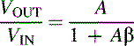
(19.1)
 |
| Figure 19.1 Canonical form of a feedback system with positive or negative feedback. |
Oscillators do not require an externally applied input signal but instead use some fraction of the output signal created by the feedback network as the input signal. It is the noise voltage that provides the initial boost signal to the circuit when positive feedback is employed. Over a period of time, the output builds up, oscillating at the frequency set by the circuit components [1].
Oscillation results when the feedback system is not able to find a stable state because its transfer function cannot be satisfied. The system becomes unstable when the denominator in Equation (19.1) is 0. When (1 + Aβ) = 0, Aβ = –1. The key to designing an oscillator, then, is to ensure that Aβ = –1. This is called the Barkhausen criterion. This constraint requires the magnitude of the loop gain be 1 with a corresponding phase shift of 180°, as indicated by the minus sign. An equivalent expression using complex math is Aβ = 1∠–180° for a negative feedback system. For a positive feedback system, the expression becomes Aβ = 1∠0° and the sign is negative in Equation (19.1).
Once the phase shift is 180° and Aβ = |1|, the output voltage of the unstable system heads for infinite voltage in an attempt to destroy the world and is prevented from succeeding only by an energy limited power supply. When the output voltage approaches either power rail, the active devices in the amplifiers change gain, causing the value of A to change so the value of Aβ ≠ 1; therefore the charge to infinite voltage slows down and eventually halts. At this point, one of three things can occur. First, nonlinearity in saturation or cutoff can cause the system to become stable and lock up at the power rail. Second, the initial charge can cause the system to saturate (or cut off) and stay that way for a long time before it becomes linear and heads for the opposite power rail. Third, the system stays linear and reverses direction, heading for the opposite power rail. Alternative 2 produces highly distorted oscillations (usually quasi square waves), and the resulting oscillators are called relaxation oscillators. Alternative 3 produces sine wave oscillators.
19.3. Phase Shift in the Oscillator
The 180° phase shift in the equation Aβ = 1∠–180° is introduced by active and passive components. Like any well designed feedback circuit, oscillators are made dependent on passive component phase shift, because it is accurate and almost drift free. The phase shift contributed by active components is minimized because it varies with temperature, has a wide initial tolerance, and is device dependent. Amplifiers are selected such that they contribute little or no phase shift at the oscillation frequency. These constraints limit the op amp oscillator to relatively low frequencies.
A single pole RL or RC circuit contributes up to 90° phase shift per pole, and because 180° of phase shift is required for oscillation, at least two poles must be used in the oscillator design. An LC circuit has two poles, thus it contributes up to 180° phase shift per pole pair. But LC and LR oscillators are not considered here because low frequency inductors are expensive, heavy, bulky, and very nonideal. LC oscillators are designed in high frequency applications, beyond the frequency range of voltage feedback op amps, where the inductor size, weight, and cost are less significant. Multiple RC sections are used in low frequency oscillator design in lieu of inductors.
Phase shift determines the oscillation frequency because the circuit oscillates at the frequency that accumulates 180° phase shift. The rate of change of phase with frequency, dφ/dω, determines frequency stability. When buffered RC sections (an op amp buffer provides high input and low output impedance) are cascaded, the phase shift multiplies by the number of sections, n (see Figure 19.2).
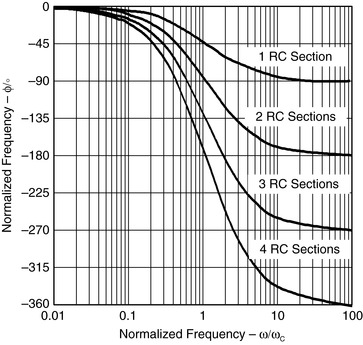 |
| Figure 19.2 Phase plot of RC sections. |
The frequency of oscillation is very dependent on the change in phase at the point where the phase shift is 180°. A tight frequency specification requires a large change in phase shift, dφ, for a small change in frequency, dω, at 180°. Figure 19.2 demonstrates that, although two cascaded RC sections eventually provide 180° phase shift, dφ/dω at the oscillator frequency is unacceptably low. Thus, oscillators made with two cascaded RC sections have poor frequency stability. Three equal cascaded RC filter sections have a much higher dφ/dω (see Figure 19.2), and the resulting oscillator has improved frequency stability. Adding a fourth RC section produces an oscillator with an excellent dφ/dω (see Figure 19.2); so this is the most stable RC oscillator configuration. Four sections are the maximum number used because op amps come in quad packages, and the four section oscillator section yields four sine waves 45° phase shifted relative to each other. This oscillator can be used to obtain sine/cosine or quadrature sine waves.
Crystal or ceramic resonators make the most stable oscillators, because resonators have an extremely high dφ/dω resulting from their nonlinear properties. Resonators are used for high frequency oscillators, but low frequency oscillators do not use resonators because of size, weight, and cost restrictions. Op amps are not generally used with crystal or ceramic resonator oscillators because op amps have low bandwidth. Experience shows that it is more cost effective to build a high frequency crystal oscillator, count the output down, and filter the output to obtain a low frequency than it is to use a low frequency resonator.
19.4. Gain in the Oscillator
The oscillator gain must equal 1 (Aβ = 1∠–180°) at the oscillation frequency. Under normal conditions, the circuit becomes stable when the gain exceeds 1 and oscillations cease. However, when the gain exceeds 1 with a phase shift of –180°, the active device nonlinearity reduces the gain to 1 and the circuit oscillates. The nonlinearity happens when the amplifier swings close to either power rail because cutoff or saturation reduces the active device (transistor) gain. The paradox is that worst case design practice requires nominal gains exceeding 1 for manufacturability, but excess gain causes more distortion of the output sine wave.
When the gain is too low, oscillations cease under worst case conditions; and when the gain is too high, the output waveform looks more like a square wave than a sine wave. Distortion is a direct result of excess gain overdriving the amplifier; hence gain must be carefully controlled in low distortion oscillators. Phase shift oscillators have distortion, but they achieve low distortion output voltages because cascaded RC sections act as distortion filters. Also, buffered phase shift oscillators have low distortion because the gain is controlled and distributed among the buffers.
Most circuit configurations require an auxiliary circuit for gain adjustment when low distortion outputs are desired. Auxiliary circuits range from inserting a nonlinear component in the feedback loop, to automatic gain control (AGC) loops, to limiting by external components such as resistors and diodes. Consideration must also be given to the change in gain due to temperature variations and component tolerances, and the level of circuit complexity is determined based on the required stability of the gain. The more stable the gain, the better the purity of the sine wave output.
19.5. Active Element (Op Amp) Impact on the Oscillator
Up to this point it has been assumed that the op amp has an infinite bandwidth and the output is not frequency dependent. In reality, the loop gain, Aβ, of the circuit is frequency dependent. Figure 19.3 shows the typical gain versus frequency response of op amps. Dividing the numerator and denominator of Equation 19.1 by Aβ yields Equation 19.2, the closed loop gain (ACL), where 1/β represents the ideal closed loop gain (ACLideal). Normally, the bandwidth of the system is specified where ACLideal intersects the open loop gain (AOL) rolloff. This is the point, f0, where ACLideal is attenuated by 3 dB and is normally drooping at a rate of 20 dB per decade. Even worse, the phase shift contributed by the op amp is 45° at this point. This is true at whatever point the gain of the circuit intercepts the open loop gain rolloff of the op amp. Clearly this region of operation must either be avoided or be compensated for by the circuit. 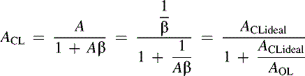
(19.2)
 |
| Figure 19.3 Op amp frequency response. |
Most op amps are compensated and may have more than the 45° of phase shift at ω3dB. The op amp should therefore be chosen with a gain bandwidth that is at least one decade above the oscillation frequency, as shown by the shaded area of Figure 19.3. The Wien bridge requires a gain bandwidth greater than 43ωOSC to maintain the gain and frequency within 10% of the ideal values [2]. Figure 19.4 compares the output distortion versus frequency of an LM328, a TLV247X, and a TLC071 op amp, which have bandwidths of 0.4 MHz, 2.8 MHz, and 10 MHz, respectively. In a Wien bridge oscillator with nonlinear feedback (see Section 19.7.1 for the circuit and transfer function), the oscillation frequency ranges from 16 Hz to 160 kHz. The graph illustrates the importance of choosing the correct op amp for the application. The LM328 achieves a maximum oscillation of 72 kHz and is attenuated more than 75%, while the TLV247X achieves 125 kHz with 18% attenuation. The wide bandwidth of the TLC071 provides a 138 kHz oscillation frequency with a mere 2% attenuation. The op amp must be chosen with the proper bandwidth or the output may oscillate at a frequency well below the design specification.
 |
| Figure 19.4 Op amp bandwidth and oscillator output. |
Care must be taken when using large feedback resistors, since they interact with the input capacitance of the op amp to create poles with negative feedback and both poles and zeros with positive feedback. Large resistor values can move these poles and zeros into the proximity of the oscillation frequency and affect the phase shift [3].
A final consideration is given to the slew rate limitation of the op amp. The slew rate must be greater than 2πVPf0, where VP is the peak output voltage and f0 is the oscillation frequency, or distortion of the output signal will result.
19.6. Analysis of the Oscillator Operation (Circuit)
Oscillators are created using various combinations of positive and negative feedback. Figure 19.5 shows the basic negative feedback amplifier block diagram with a positive feedback loop added. When positive and negative feedback are used, the gain of the negative feedback path is combined into one gain term (representing the closed loop gain) and Figure 19.5 reduces to Figure 19.1. The positive feedback network is then represented by β = β2, and subsequent analysis is simplified. When negative feedback is used, the positive feedback loop can be ignored, since β2 is 0. The case of positive and negative feedback combined is covered here, since the negative feedback case was reviewed in Chapter 6 and Chapter 7.
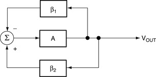 |
| Figure 19.5 Block diagram of an oscillator. |
A general form of an op amp with positive and negative feedback is shown in Figure 19.6(a). The first step is to break the loop at some point without altering the gain of the circuit. The positive feedback loop is broken at the point marked with an X. A test signal (VTEST) is applied to the broken loop and the resulting output voltage (VOUT) is measured with the equivalent circuit shown in Figure 19.6(b).
 |
| Figure 19.6 Amplifier with positive and negative feedback. |
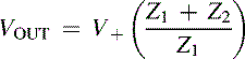
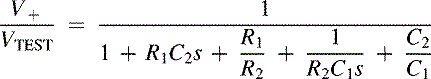
V+ is calculated first in Equation (19.3), then is treated as an input signal to a noninverting amplifier, resulting in Equation (19.4). Equation (19.3) is substituted for V+ in Equation (19.4) to get the transfer function in Equation (19.5). The actual circuit elements are then substituted for each impedance and the equation is simplified. These equations are valid when the op amp open loop gain is large and the oscillation frequency is <0.1 ω3dB.

(19.3)
(19.4)
(19.5)
Phase shift oscillators generally use negative feedback, so the positive feedback factor (β2) becomes zero. Oscillator circuits such as the Wien bridge use both negative (β1) and positive (β2) feedback to achieve a constant state of oscillation. This circuit is analyzed in detail in Section 19.7.1 using Equation (19.5).
19.7. Sine Wave Oscillator Circuits
There are many types of sine wave oscillator circuits and variations of these circuits—the choice depends on the frequency and the desired purity of the output waveform. The focus of this section is on the more prominent oscillator circuits: Wien bridge, phase shift, and quadrature. The transfer function is derived for each case using the techniques described in Section 19.6 of this chapter and in Chapter 3, Chapter 6 and Chapter 7.
19.7.1. Wien Bridge Oscillator
The Wien bridge is one of the simplest and best known oscillators and is used extensively in circuits for audio applications. Figure 19.7 shows the basic Wien bridge circuit configuration. This circuit has only a few components and good frequency stability. The major drawback of the circuit is that the output amplitude is at the rails, saturating the op amp output transistors and causing high output distortion. Taming this distortion is more of a challenge than getting the circuit to oscillate. A couple of ways may be used to minimize this effect, which is covered later. It is now time to analyze this circuit and come up with the transfer function.
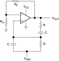 |
| Figure 19.7 Wien bridge circuit schematic. |
The Wien bridge circuit is of the form detailed in Section 19.6. The transfer function for the circuit is created using the technique described in that section. It is readily apparent that Z1 = RG, Z2 = RF, Z3 = (R1 + 1/sC1), and Z4 = (R2‖ 1/sC2). The loop is broken between the output and Z1, VTEST is applied to Z1, and VOUT is calculated. The positive feedback voltage, V+, is calculated first in Equations (19.6) through (19.8). Equation (19.6) shows the simple voltage divider at the noninverting input. Each term is then multiplied by (R2C2s + 1) and divided by R2 to get Equation (19.7).
(19.6)
(19.7)
Substitute s = jω0, where ω0 is the oscillation frequency, ω1 = 1/R1C2, and ω2 = 1/R2C1 to get Equation (19.8):
(19.8)
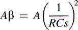
Some interesting relationships now become apparent. The capacitor in the zero, represented by ω1, and the capacitor in the pole, represented by ω2, must each contribute 90° of phase shift toward the 180° required for oscillation at ω0. This requires that C1 = C2 and R1 = R2. Setting ω1 and ω2 equal to ω0 cancels the frequency terms, ideally removing any change in amplitude with frequency, since the pole and zero negate one another. An overall feedback factor of β = 1/3 is the result, Equation (19.9):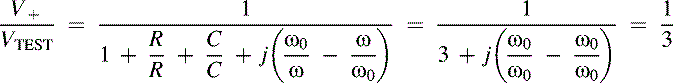
(19.9)
The gain of the negative feedback portion, A, of the circuit must then be set such that |Aβ| = 1, requiring A = 3. RF must be set to twice the value of RG to satisfy the condition. The op amp in Figure 19.7 is single supply, so a DC reference voltage, VREF, must be applied to bias the output for full scale swing and minimal distortion. Applying VREF to the positive input through R2 restricts DC current flow to the negative feedback leg of the circuit. VREF is set at 0.833V to bias the output at the midrail of the single supply, rail to rail input, and output amplifier, or 2.5 V. See Chapter 4 for details on DC biasing single supply op amps. VREF is shorted to ground for split supply applications.
The final circuit is shown in Figure 19.8, with component values selected to provide an oscillation frequency of ω0 = 2πf0, where f0 = 1/(2πRC) = 19.9 kHz. The circuit oscillated at 1.57 kHz due to slightly varying component values with 2% distortion. This high value is due to the extensive clipping of the output signal at both supply rails, producing several large odd and even harmonics. The feedback resistor was then adjusted ±1%. Figure 19.9 shows the output voltage waveforms. The distortion grows as the saturation increases with increasing RF, and oscillations cease when RF is decreased by more than 0.8%.
 |
| Figure 19.8 Final Wien bridge oscillator circuit. |
 |
| Figure 19.9 Wien bridge output waveforms. |
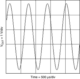
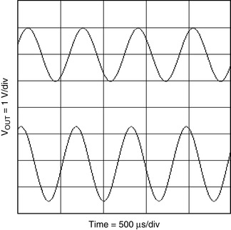
Applying nonlinear feedback can minimize the distortion inherent in the basic Wien bridge circuit. A nonlinear component, such as an incandescent lamp, can be substituted into the circuit for RG, as shown in Figure 19.10. The lamp resistance, RLAMP, is nominally selected as half the feedback resistance, RF, at the lamp current established by RF and RLAMP. When the power is first applied, the lamp is cool and its resistance is small, so the gain is large (>3). The current heats the filament and the resistance increases, lowering the gain. The nonlinear relationship between the lamp current and resistance keeps output voltage changes small. Figure 19.11 shows the output of this amplifier with a distortion of 1% for fOSC = 1.57 kHz. The distortion for this variation is reduced over the basic circuit by avoiding hard saturation of the op amp transistors.
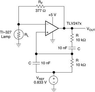 |
| Figure 19.10 Wien bridge oscillator with nonlinear feedback. |
 |
| Figure 19.11 Output of the circuit in Figure 19.10. |
The impedance of the lamp is due mostly to thermal effects. The output amplitude is then very temperature sensitive and tends to drift. The gain must be set higher than 3 to compensate for any temperature variations, which increases the distortion in the circuit [4]. This type of circuit is useful when the temperature does not fluctuate over a wide range or when used in conjunction with an amplitude limiting circuit.
The lamp has an effective low frequency thermal time constant, tthermal [5]. As fOSC approaches tthermal, distortion is greatly increased. Several lamps can be placed in series to increase tthermal and reduce distortion. The drawbacks are that the time required for oscillations to stabilize is increased and the output amplitude is reduced.
An automatic gain control circuit must be used when neither of the two previous circuits yield low distortion. A typical Wien bridge oscillator with an AGC circuit is shown in Figure 19.12, with the output waveform of the circuit shown in Figure 19.13. The AGC is used to stabilize the magnitude of the sinusoidal output to an optimum gain level. The JFET serves as the AGC element, providing excellent control because of the wide range of the drain to source resistance (RDS), which is controlled by the gate voltage. The JFET gate voltage is 0 V when the power is applied, and the JFET turns on with low RDS. This places RG2 + RS + RDS in parallel with RG1, raising the gain to 3.05, and oscillations begin and gradually build up. As the output voltage gets large, the negative swing turns the diode on and the sample is stored on C1, which provides a DC potential to the gate of Q1. Resistor R1 limits the current and establishes the time constant for charging C1, which should be much greater than fOSC. When the output voltage drifts high, RDS increases, lowering the gain to a minimum of 2.87 (1 + RF/RG1). The output stabilizes when the gain reaches 3. The distortion of the AGC is 0.8%, which is due to slight clipping at the positive rail.
 |
| Figure 19.12 Wien bridge oscillator with AGC. |
 |
| Figure 19.13 Output of the circuit in Figure 19.12. |
The circuit of Figure 19.12 is biased with VREF for a single supply amplifier. A zener diode can be placed in series with D1 to limit the positive swing of the output and reduce distortion. A split supply can be easily implemented by grounding all points connected to VREF. A wide variety of Wien bridge variations exist to more precisely control the amplitude and allow selectable or even variable oscillation frequencies. Some circuits use diode limiting in place of a nonlinear feedback component. The diodes reduce the distortion by providing a soft limit for the output voltage.
19.7.2. Phase Shift Oscillator, Single Amplifier
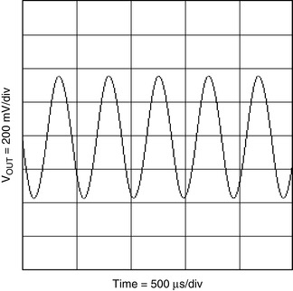
Phase shift oscillators have less distortion than the Wien bridge oscillator, coupled with good frequency stability. A phase shift oscillator can be built with one op amp as shown in Figure 19.14; the resulting output waveform is in Figure 19.15. Three RC sections are cascaded to get the steep dφ/dω slope, as described in Section 19.3, to get a stable oscillation frequency. Any less and the oscillation frequency is high and interferes with the op amp BW limitations.
 |
| Figure 19.14 Phase shift oscillator (single op amp). |
 |
| Figure 19.15 Output of the circuit in Figure 19.14. |
The normal assumption is that the phase shift sections are independent of each other. Then Equatiotn (19.10) is written: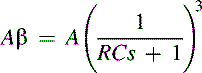
(19.10)
The loop phase shift is –180° when the phase shift of each section is –60°, and this occurs when ω = 2πf = 1.732/RC because the tangent of 60° = 1.732. The magnitude of β at this point is (1/2)3, so the gain, A, must be equal to 8 for the system gain to be equal to 1.
The oscillation frequency with the component values shown in Figure 19.14 is 3.76 kHz rather than the calculated oscillation frequency of 2.76 kHz. Also, the gain required to start oscillation is 27 rather than the calculated gain of 8. These discrepancies are partially due to component variations, but the biggest contributing factor is the incorrect assumption that the RC sections do not load each other. This circuit configuration was very popular when active components were large and expensive. But now op amps are inexpensive, small, and come four in a package, so the single op amp phase shift oscillator is losing popularity. The output distortion is a low 0.46%, considerably less than the Wein bridge circuit without amplitude stabilization.
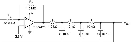
19.7.3. Phase Shift Oscillator, Buffered
The buffered phase shift oscillator is much improved over the unbuffered version, the cost being a higher component count. The buffered phase shift oscillator is shown in Figure 19.16 and the resulting output waveform in Figure 19.17. The buffers prevent the RC sections from loading each other, hence the buffered phase shift oscillator performs closer to the calculated frequency and gain. The gain setting resistor, RG, loads the third RC section. If the fourth buffer in a quad op amp buffers this RC section, the performance becomes ideal. Low distortion sine waves can be obtained from either phase shift oscillator design, but the purest sine wave is taken from the output of the last RC section. This is a high impedance node, so a high impedance input is mandated to prevent loading and frequency shifting with load variations.
 |
| Figure 19.16 Phase shift oscillator, buffered. |
 |
| Figure 19.17 Output of the circuit in Figure 19.16. |
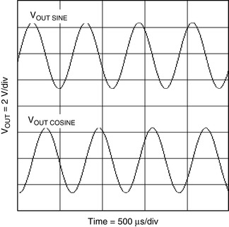
19.7.4. Bubba Oscillator
The bubba oscillator in Figure 19.18 is another phase shift oscillator, but it takes advantage of the quad op amp package to yield some unique advantages. Four RC sections require 45° phase shift per section, so this oscillator has an excellent dφ/dt, resulting in minimized frequency drift. The RC sections each contribute 45° phase shift, so taking outputs from alternate sections yields low impedance quadrature outputs. When an output is taken from each op amp, the circuit delivers four 45° phase shifted sine waves. The loop equation is given in Equation (19.11). When ω = 1/RCs, Equation (19.11) reduces to (19.12) and (19.13):

(19.11)
(19.12)
(19.13)
 |
| Figure 19.18 Bubba oscillator. |
The gain, A, must equal 4 for oscillation to occur. The test circuit oscillated at 1.76 kHz rather than the ideal frequency of 1.72 kHz when the gain was 4.17 rather than the ideal gain 4. The output waveform is shown in Figure 19.19. Distortion is 1% for VOUTSINE and 0.1% for VOUTCOSINE. With low gain A and low bias current op amps, the gain setting resistor, RG, does not load the last RC section, thus ensuring oscillator frequency accuracy. Very low distortion sine waves can be obtained from the junction of R and RG. When low distortion sine waves are required at all outputs, the gain should be distributed among all the op amps. The noninverting input of the gain op amp is biased at 0.5 V to set the quiescent output voltage at 2.5 V for single supply operation and should be ground for split supply op amps. Gain distribution requires biasing of the other op amps, but it has no effect on the oscillator frequency.
 |
| Figure 19.19 Output of the circuit in Figure 19.18. |
19.7.5. Quadrature Oscillator
The quadrature oscillator shown in Figure 19.20 is another type of phase shift oscillator, but the three RC sections are configured so each section contributes 90° of phase shift. This provides both sine and cosine waveform outputs (the outputs are quadrature, or 90° apart), which is a distinct advantage over other phase shift oscillators. The idea of the quadrature oscillator is to use the fact that the double integral of a sine wave is a negative sine wave of the same frequency and phase. The phase of the second integrator is then inverted and applied as positive feedback to induce oscillation [6].
 |
| Figure 19.20 Quadrature oscillator. |
The loop gain is calculated in Equation (19.14). When R1C1 = R2C2 = R3C3, Equation (19.14) reduces to Equation (19.15). When ω = 1/RC, Equation (19.14) reduces to 1∠–180, so oscillation occurs at ω = 2πf = 1/RC. The test circuit oscillated at 1.65 kHz rather than the calculated 1.59 kHz, as shown in Figure 19.21. This discrepancy is attributed to component variations. Both outputs have relatively high distortion that can be reduced with a gain stabilizing circuit. The sine output had 0.846% distortion and the cosine output had 0.46% distortion. Adjusting the gain can increase the amplitudes. The cost is bandwidth.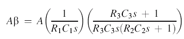
(19.14)
(19.15)
 |
| Figure 19.21 Output of the circuit in Figure 19.20. |
19.8. Conclusion
Op amp oscillators are restricted to the lower end of the frequency spectrum because they do not have the required bandwidth to achieve low phase shift at high frequencies. The new current feedback op amps have a much greater bandwidth than the voltage feedback op amps but are very difficult to use in oscillator circuits because of their sensitivity to feedback capacitance. Voltage feedback op amps are limited to tens of hertz (at the most!) because of their low frequency roll-off. The bandwidth is reduced when op amps are cascaded due to the multiple contribution of phase shift.
The Wien bridge oscillator has few parts and good frequency stability, but the basic circuit has a high output distortion. AGC improves the distortion considerably, particularly at the lower frequency range. Nonlinear feedback offers the best performance over the middle and upper frequency ranges. The phase shift oscillator has lower output distortion and, without buffering, requires a high gain, which limits the use to very low frequencies. Decreasing cost of op amps and components has reduced the popularity of the phase shift oscillators. The quadrature oscillator requires only two op amps, has reasonable distortion, and offers both sine and cosine waveforms. The drawback is the low amplitude, which may require a higher gain and a reduction in bandwidth, or an additional gain stage.
May your oscillators always oscillate, and your amplifiers always amplify.
References
1. Irving M. Gottlieb, Practical Oscillator Handbook. (1997) Newnes, Boston.
2. E.J. Kennedy, Operational Amplifier Circuits, Theory and Applications. (1988) Holt Rinehart and Winston, New York.
3. Jerald Graeme, Optimizing Op Amp Performance. (1997) McGraw-Hill, New York.
4. Philbrick Researches, Inc., Applications Manual for Computing Amplifiers. (1966) Nimrod Press.
5. Rudolf F. Graf, Oscillator Circuits. (1997) Newnes, Boston.
6. Jerald Graeme, Applications of Operational Amplifiers, Third Generation Techniques. (1973) McGraw-Hill, New York.
..................Content has been hidden....................
You can't read the all page of ebook, please click here login for view all page.