
6
POWER-FACTOR-CORRECTION (PFC) CIRCUITS AND DESIGNING THE FEEDBACK CONTROLLER
In diode rectifiers discussed in Chapter 5, power is drawn by means of highly distorted currents, which have a deleterious effect on the power quality of the utility source. In single-phase diode-rectifier systems, a corrective action such as that described in this chapter is often taken. This discussion is also useful in the learning process since it shows a real-world application of DC-DC converters discussed in Chapter 3 and their control in Chapter 4.
6.1 INTRODUCTION
Technical solutions to the problem of distortion in the input current have been known for a long time. However, only recently has the concern about the deleterious effects of harmonics led to the formulation of guidelines and standards, which in turn have focused attention on ways of limiting current distortion.
In the following sections, power-factor-corrected (PFC) interface, as they are often called, are briefly examined for single-phase rectification, where it is assumed that the power needs to flow only in one direction, such as in DC power supplies. The three-phase front-ends in motor-drives applications may require bi-directional power flow capability. Such front-ends, which also allow unity power factor of operation, are discussed in Chapter 12.
6.2 OPERATING PRINCIPLE OF SINGLE-PHASE PFCS
The operating principle of a commonly used single-phase PFC is shown in Figure 6.1a, where, between the utility supply and the DC-bus capacitor, a boost DC-DC converter is introduced. This boost converter consists of a MOSFET, a diode, and a small inductor ![]() . By pulse-width-modulating the MOSFET at a constant switching frequency, the current
. By pulse-width-modulating the MOSFET at a constant switching frequency, the current ![]() through the inductor
through the inductor ![]() is shaped to have the full-wave-rectified waveform
is shaped to have the full-wave-rectified waveform ![]() , similar to
, similar to ![]() , as shown in Figure 6.1b.
, as shown in Figure 6.1b.
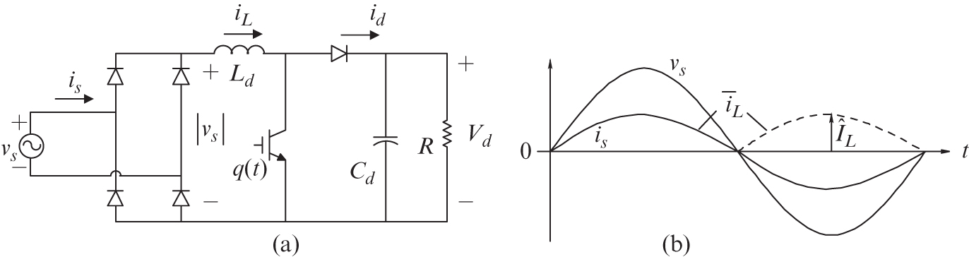
FIGURE 6.1 PFC circuit and waveforms.
The inductor current contains a high switching-frequency ripple, which is removed by a small filter.
The input current ![]() in the circuit of Figure 6.1a becomes sinusoidal and in phase with the supply voltage. In the boost converter, it is essential that the DC-bus voltage
in the circuit of Figure 6.1a becomes sinusoidal and in phase with the supply voltage. In the boost converter, it is essential that the DC-bus voltage ![]() be greater than the peak of the supply voltage
be greater than the peak of the supply voltage ![]() :
:
Figure 6.2a shows the average model of the boost converter in the continuous-conduction mode (CCM) with ![]() at all times. Neglecting a small voltage drop across the inductor and assuming the voltage across the capacitor to be a pure DC, in a boost converter, the voltage transfer ratio is
at all times. Neglecting a small voltage drop across the inductor and assuming the voltage across the capacitor to be a pure DC, in a boost converter, the voltage transfer ratio is

FIGURE 6.2 Average model in CCM (Average model in CCM (
and thus,
and
Equation (6.3) shows that ![]() of the switch varies sinusoidally during each half-cycle of the fundamental frequency, independent of the value of the inductor current, provided it is greater than zero. The switch duty ratio from Equation (6.3b) is plotted in Figure 6.2b.
of the switch varies sinusoidally during each half-cycle of the fundamental frequency, independent of the value of the inductor current, provided it is greater than zero. The switch duty ratio from Equation (6.3b) is plotted in Figure 6.2b.
The inductor current is shaped to be ![]() . Therefore, the current
. Therefore, the current ![]() can be calculated from the turns ratio of the ideal transformer in Figure 6.2a as
can be calculated from the turns ratio of the ideal transformer in Figure 6.2a as
Substituting for ![]() from Equation (6.3) in Equation (6.4),
from Equation (6.3) in Equation (6.4),
Recognizing that in Equation (6.4), ![]() :
:
 (6.5)
(6.5)
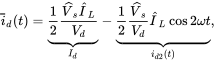
Equation (6.5) shows that the average current to the output stage consists of a DC component ![]() and a component
and a component ![]() at the second-harmonic frequency.
at the second-harmonic frequency.
Example 6.1
Derive ![]() in Equation (6.5) by equating input and output powers.
in Equation (6.5) by equating input and output powers.
Solution Assume that ![]() and
and ![]() . Therefore, the input power
. Therefore, the input power ![]() . Recognizing that
. Recognizing that ![]() , the input power is
, the input power is ![]() . The output power
. The output power ![]() . Equating
. Equating ![]() , and recognizing that
, and recognizing that ![]()
 (6.6)
(6.6)
which is the same as Equation (6.5).
The output stage of the PFC is shown in Figure 6.3, where the DC component ![]() of
of ![]() flows through the load-equivalent resistor. In PFCs, the capacitor in the output stage is quite large, such that it is justifiable to approximate that the second-harmonic frequency component
flows through the load-equivalent resistor. In PFCs, the capacitor in the output stage is quite large, such that it is justifiable to approximate that the second-harmonic frequency component ![]() flows entirely through the output capacitor and none through the load-equivalent resistor. The peak value of
flows entirely through the output capacitor and none through the load-equivalent resistor. The peak value of ![]() is
is

FIGURE 6.3 Current division in the output stage.
Based on the assumption that ![]() flows entirely through the output capacitor, the peak value of the second-harmonic frequency ripple in the output voltage can be calculated as follows, where the reactance of the capacitor at twice the line frequency is
flows entirely through the output capacitor, the peak value of the second-harmonic frequency ripple in the output voltage can be calculated as follows, where the reactance of the capacitor at twice the line frequency is ![]() :
:
![]() depends inversely on the output capacitance
depends inversely on the output capacitance ![]() , and therefore, an appropriate value of
, and therefore, an appropriate value of ![]() must be chosen to minimize this ripple.
must be chosen to minimize this ripple.
Example 6.2
Calculate ![]() at full-load and the nominal input voltage for the parameters and operating values of a PFC given in Table 6.1 later on. Ignore the capacitor ESR.
at full-load and the nominal input voltage for the parameters and operating values of a PFC given in Table 6.1 later on. Ignore the capacitor ESR.
Solution Assuming the PFC to be lossless, ![]() . Therefore, using the values given in Table 6.1,
. Therefore, using the values given in Table 6.1, ![]() .
. ![]() . Therefore, from Equation (6.8), the peak value of the second-harmonic frequency voltage is
. Therefore, from Equation (6.8), the peak value of the second-harmonic frequency voltage is
TABLE 6.1 Parameters and operating values.
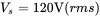
| Nominal input AC source voltage, | 120 V |
| Line frequency, | 60 Hz |
| Output voltage, | 250 V(DC) |
| Maximum power output | 250 W |
| Switching frequency, | 100 kHz |
| Output filter capacitor, | |
| ESR of the capacitor, | |
| Inductor, | |
| Full-load equivalent resistance, | |
6.3 CONTROL OF PFCS
Figure 6.4 shows the PFC power circuit along with its control circuit in a block-diagram form. In controlling a PFC, the main objective is to draw a sinusoidal current in-phase with the utility voltage. The reference inductor current ![]() is of the full-wave rectified form, similar to that in Figure 6.1b. The requirements on the form and the amplitude of the inductor current lead to two control loops, as shown in Figure 6.4, to pulse-width modulate the switch of the boost converter.
is of the full-wave rectified form, similar to that in Figure 6.1b. The requirements on the form and the amplitude of the inductor current lead to two control loops, as shown in Figure 6.4, to pulse-width modulate the switch of the boost converter.
- The average inner current control loop ensures the form of
 based on the template
  provided by measuring the rectifier output voltage
  .
. - The outer voltage control loop determines the amplitude
 of
of  based on the output voltage feedback. If the inductor current is insufficient for a given load supplied by the PFC, the output voltage will drop below its preselected reference value
  . By measuring the output voltage and using it as the feedback signal, the voltage control loop adjusts the inductor current amplitude to bring the output voltage to its reference value. In addition to determining the inductor current amplitude, this voltage feedback control acts to regulate the output voltage of the PFC to the preselected DC voltage.

FIGURE 6.4 PFC control loops.
In Figure 6.4, the inner current-control loop is required to have a very high bandwidth compared to the outer voltage-control loop. Hence, each loop can be designed separately, similar to the approach taken in the peak-current-mode control discussed in Chapter 4.
6.4 DESIGNING THE INNER AVERAGE-CURRENT-CONTROL LOOP
The inner current control loop is shown within the inner dotted box in Figure 6.4. In order to follow the reference with as little THD as possible, an average-current-mode control is used with a high bandwidth, where the error between the reference ![]() and the measured inductor current
and the measured inductor current ![]() is amplified by a current controller to produce the control voltage
is amplified by a current controller to produce the control voltage ![]() . This control voltage is compared with a ramp signal
. This control voltage is compared with a ramp signal ![]() , with a peak of
, with a peak of ![]() at the switching frequency
at the switching frequency ![]() in the PWM controller IC [1], to produce the switching signal
in the PWM controller IC [1], to produce the switching signal ![]() .
.
Just the inner current control loop of Figure 6.4 can be simplified, as shown in Figure 6.5a. The reference input ![]() varies with time, as shown in Figure 6.2b, where the corresponding
varies with time, as shown in Figure 6.2b, where the corresponding ![]() and
and ![]() waveforms are also plotted. However, these quantities vary much more slowly compared to the current control-loop bandwidth, approximately 10 kHz in the numerical example considered later on. Therefore, at each instant of time, for example at
waveforms are also plotted. However, these quantities vary much more slowly compared to the current control-loop bandwidth, approximately 10 kHz in the numerical example considered later on. Therefore, at each instant of time, for example at ![]() in Figure 6.2b, the circuit of Figure 6.2a can be considered in a “DC” steady-state with the associated variables having values of
in Figure 6.2b, the circuit of Figure 6.2a can be considered in a “DC” steady-state with the associated variables having values of ![]() ,
, ![]() and
and ![]() . This equilibrium condition varies slowly with time compared to the current-control-loop bandwidth, which is designed to be much larger. In the Laplace domain, this current loop is shown in Figure 6.5b, as discussed below, where the tilde “~” on top represents small signal perturbations at very high frequencies in the range of the current-control-loop bandwidth, for example, 10 kHz.
. This equilibrium condition varies slowly with time compared to the current-control-loop bandwidth, which is designed to be much larger. In the Laplace domain, this current loop is shown in Figure 6.5b, as discussed below, where the tilde “~” on top represents small signal perturbations at very high frequencies in the range of the current-control-loop bandwidth, for example, 10 kHz.

FIGURE 6.5 PFC current loop.
6.4.1 d˜(s)/v˜c(s) for the PWM Controller
If ![]() is the difference between the peak and the valley of the ramp voltage in the PWM-IC, then the small-signal transfer function of the PWM controller, as discussed in Chapter 4, is
is the difference between the peak and the valley of the ramp voltage in the PWM-IC, then the small-signal transfer function of the PWM controller, as discussed in Chapter 4, is
6.4.2 i˜L(s)/d˜(s) for the Boost Converter in the Power Stage
In spite of the varying DC steady-state operating point, the transfer function in the boost converter simplifies as follows at high frequencies at which the current-control-loop bandwidth is designed:
This can be observed from the small-signal circuit for the boost converters in Figure 4.7b of Chapter 4, where at high frequencies, the capacitor acts as a short circuit, resulting in the above transfer function (ignoring capacitor ESR, and noting that ![]() in Chapter 4 is
in Chapter 4 is ![]() in this chapter). This conclusion can be confirmed by LTspice simulations that show that in the boost converter of a PFC, all the curves corresponding to various input voltages and the associated duty ratios merge at high frequencies to yield results similar to that of the transfer function in Equation (6.10).
in this chapter). This conclusion can be confirmed by LTspice simulations that show that in the boost converter of a PFC, all the curves corresponding to various input voltages and the associated duty ratios merge at high frequencies to yield results similar to that of the transfer function in Equation (6.10).
6.4.3 Designing the Current Controller Gi(s)
The transfer function in Equation (6.10) is an approximation valid at high frequencies and not a pure integrator. Therefore, to have a high loop DC gain and a zero DC steady-state error in Figure 6.5b, the current controller transfer function ![]() must have a pole at the origin. In the loop in Figure 6.5b, the phase due to the pole at origin in
must have a pole at the origin. In the loop in Figure 6.5b, the phase due to the pole at origin in ![]() and that of the power-stage transfer function (Equation 6.10) add up to
and that of the power-stage transfer function (Equation 6.10) add up to![]() . Hence,
. Hence, ![]() , as in the peak-current mode control discussed in Chapter 4, includes a pole-zero pair that provides a phase boost, and hence the specified phase margin, for example
, as in the peak-current mode control discussed in Chapter 4, includes a pole-zero pair that provides a phase boost, and hence the specified phase margin, for example ![]() at the loop crossover frequency:
at the loop crossover frequency:
where ![]() is the controller gain. Knowing the phase boost,
is the controller gain. Knowing the phase boost, ![]() , we can calculate the pole-zero locations to provide the necessary phase boost, as discussed in Chapter 4:
, we can calculate the pole-zero locations to provide the necessary phase boost, as discussed in Chapter 4:
where ![]() is the crossover frequency of the current loop transfer function.
is the crossover frequency of the current loop transfer function.
6.5 DESIGNING THE OUTER VOLTAGE-CONTROL LOOP
As mentioned earlier, the outer voltage-control loop is needed to determine the peak, ![]() , of the inductor current. In this voltage loop, the bandwidth is limited to approximately 15 Hz. The reason has to do with the fact that the output voltage across the capacitor contains a component
, of the inductor current. In this voltage loop, the bandwidth is limited to approximately 15 Hz. The reason has to do with the fact that the output voltage across the capacitor contains a component ![]() as derived in Equation (6.8) at twice the line-frequency (at 120 Hz in 60-Hz line-frequency systems). This output voltage ripple must not be corrected by the voltage loop; otherwise, it will lead to a third-harmonic distortion in the input current, as explained in Appendix 6A at the end of this chapter.
as derived in Equation (6.8) at twice the line-frequency (at 120 Hz in 60-Hz line-frequency systems). This output voltage ripple must not be corrected by the voltage loop; otherwise, it will lead to a third-harmonic distortion in the input current, as explained in Appendix 6A at the end of this chapter.
In view of such a low bandwidth of the voltage-control loop (approximately three orders of magnitude below the current-loop bandwidth of ~10 kHz), it is perfectly reasonable to assume the current loop to be ideal at low frequencies around 15 Hz. Therefore, in the voltage-control block diagram shown in Figure 6.6a, the current closed-loop produces ![]() equal to its reference value
equal to its reference value![]() . In addition to a large DC component,
. In addition to a large DC component, ![]() contains an unwanted second-harmonic frequency component
contains an unwanted second-harmonic frequency component ![]() due to
due to ![]() in the input to the voltage controller.
in the input to the voltage controller. ![]() at the second-harmonic frequency results in a third-harmonic frequency distortion in the current drawn from the utility, as explained in Appendix 6A. Therefore, in the output of the voltage controller block in Figure 6.6a,
at the second-harmonic frequency results in a third-harmonic frequency distortion in the current drawn from the utility, as explained in Appendix 6A. Therefore, in the output of the voltage controller block in Figure 6.6a, ![]() is limited to approximately 1.5% of the DC component in
is limited to approximately 1.5% of the DC component in ![]() .
.

FIGURE 6.6 Voltage control loop.
The voltage control loop for low-frequency perturbations, in the range of the voltage-loop bandwidth of approximately 15 Hz, is shown in Figure 6.6b. As derived in Appendix 6B, the transfer function of the power stage in Figure 6.6b at these low perturbation frequencies (ignoring the capacitor ESR) is:
To achieve a zero steady-state error, the voltage-controller transfer function should have a pole at the origin. However, since the PFC circuit is often a pre-regulator (not a strict regulator), this requirement is waived, which otherwise would make the voltage controller design much more complicated. The following simple transfer function is often used for the voltage controller in Figure 6.6b, where a pole is placed at the voltage-loop crossover frequency ![]() (yet to be determined) below 15 Hz,
(yet to be determined) below 15 Hz,
At full load, the power stage transfer function given by Equation (6.15) has a pole at a very low frequency, for example, of the order of one or two Hz, which introduces a phase lag approaching 90° much beyond the frequency at which this pole occurs. The transfer function of the controller given by Equation (6.16) introduces a lag of 45° at the loop crossover frequency. Therefore, the sum of these two phase lags adds to ![]() at the crossover frequency and results in a satisfactory phase margin of
at the crossover frequency and results in a satisfactory phase margin of ![]() . Using Equations (6.15) and (6.16), by definition, at the crossover frequency
. Using Equations (6.15) and (6.16), by definition, at the crossover frequency ![]() , the loop transfer function in Figure 6.6b has a magnitude equal to unity:
, the loop transfer function in Figure 6.6b has a magnitude equal to unity:
In the voltage controller of Figure 6.6b and Equation (6.16), the input ![]() results in an output
results in an output ![]() . Therefore, at the second-harmonic frequency in the voltage controller of Equation (6.16),
. Therefore, at the second-harmonic frequency in the voltage controller of Equation (6.16),
From Equations (6.17) and (6.18), the two unknowns ![]() and
and ![]() in the voltage controller transfer function of Equation (6.16) can be calculated, as described by a numerical example.
in the voltage controller transfer function of Equation (6.16) can be calculated, as described by a numerical example.
6.6 EXAMPLE OF SINGLE-PHASE PFC SYSTEMS
The operation and control of a PFC are demonstrated by means of an example, where the parameters are as shown in Table 6.1, and the total harmonic distortion in the input line current is required to be less than 3% [1, 2]:
6.6.1 Design of the Current-Control Loop
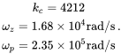
In Equation (6.9), assume that ![]() . Following the procedure described in Chapter 4 for the peak-current-mode control of DC-DC converters, for the loop crossover frequency of 10 kHz(
. Following the procedure described in Chapter 4 for the peak-current-mode control of DC-DC converters, for the loop crossover frequency of 10 kHz(![]() ) and the phase margin of
) and the phase margin of ![]() , the parameters in the current controller of Equation (6.11) are as follows:
, the parameters in the current controller of Equation (6.11) are as follows:
 (6.19)
Based on these parameter values given in Equation (6.19) of the transfer function ![]() in Equation (6.11), the op-amp circuit is similar to that in Figure 4.19 in Chapter 4 with the following values for a chosen value of
in Equation (6.11), the op-amp circuit is similar to that in Figure 4.19 in Chapter 4 with the following values for a chosen value of ![]() :
:
 (6.20)
6.6.2 Design of the Voltage-Control Loop
In this example, at full load, the plant transfer function given by Equation (6.15) has a pole at the frequency of 36.36 rad/s (5.79 Hz). At full load, ![]() , and in Equation (6.8),
, and in Equation (6.8), ![]() . Based on the previous discussion, the second-harmonic component is limited to 1.5% of
. Based on the previous discussion, the second-harmonic component is limited to 1.5% of ![]() , such that
, such that ![]() . Using these values, from Equations (6.17) and (6.18), the parameters in the voltage controller transfer function of Equation (6.16) are calculated:
. Using these values, from Equations (6.17) and (6.18), the parameters in the voltage controller transfer function of Equation (6.16) are calculated: ![]() , and
, and ![]() (11.73 Hz). This transfer function is realized by an op-amp circuit shown in Figure 6.7, where
(11.73 Hz). This transfer function is realized by an op-amp circuit shown in Figure 6.7, where
 (6.21)

FIGURE 6.7 Op-amp circuit to implement transfer function Gv(s).
6.7 SIMULATION RESULTS
The LTspice-based simulation of the PFC system is shown in Figure 6.8, where the input voltage and the full-bridge rectifier are combined for simplification purposes. The output load is decreased as a step at 100 ms. The resulting waveforms for the voltage and the inductor current are shown in Figure 6.9.

FIGURE 6.8 LTspice simulation diagram (the load is decreased at 100 ms); for a better resolution, execute the LTspice Schematic on the accompanying website.

FIGURE 6.9 Simulation results: output voltage and inductor current.
6.8 FEEDFORWARD OF THE INPUT VOLTAGE
The input voltage is fed forward, as shown in Figure 6.10. In a system with a PFC interface, the output is nearly constant, independent of the changes in the RMS value of the input voltage from the utility. Therefore, an increase in the utility voltage ![]() causes a decrease in
causes a decrease in ![]() , and vice versa. To avoid propagating the input voltage disturbance through the PFC feedback loops, the input voltage peak is fed forward, as shown in Figure 6.10, in determining
, and vice versa. To avoid propagating the input voltage disturbance through the PFC feedback loops, the input voltage peak is fed forward, as shown in Figure 6.10, in determining ![]() .
.

FIGURE 6.10 Feedforward of the input voltage.
6.9 OTHER CONTROL METHODS FOR PFCS
In this book, an average-current-control method is described for controlling PFCs. There are other methods, such as a single-cycle control. The reader is referred to References 4 and 5 for further exploration.
REFERENCES
- 1. Philip C. Todd, “UC3854 Controlled Power Factor Correction Circuit Design,” Unitrode Application Note U-134.
- 2. Lyod Dixon, “High Power Factor Switching Pre-Regulator Design Optimization,” Unitrode Design Application Manual.
PROBLEMS
- 6.1 In a single phase, 60-Hz power factor correction circuit,
 ,
,  , and the output power is 300 W. Calculate and draw the following waveforms, synchronized to
  waveform:
  ,
,  , and the average current
  through the output diode.
 - 6.2 In the numerical example given in this chapter, calculate the RMS input current if the utility voltage is
 , and compare it with its nominal value when
  .
. - 6.3 In problem 6.1, calculate the second-harmonic peak voltage in the capacitor if
 .
. - 6.4 In the numerical example given in this chapter, calculate the maximum peak-peak ripple current in the inductor.
- 6.5 Repeat the design of the current loop in the given numerical example in this chapter if the loop crossover frequency is
 .
. - 6.6 Repeat the design of the outer voltage loop in the numerical example given in this chapter if the output capacitance
 .
.
Simulation Problem
- 6.7 In the simulation diagram of Figure 6.8:
- Observe the input voltage to the boost converter (output of the diode-rectifier bridge, not modeled here), the inductor current, and the voltage across the load.
- List the harmonic components of the inductor current
 and the capacitor current
  .
. - Confirm the validity of Equation (6.5) for the current into the output stage of the PFC.
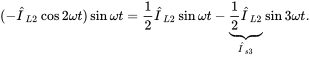
APPENDIX 6A Proof that 
The output of the voltage regulator ![]() in Figure 6.6b in steady state is
in Figure 6.6b in steady state is
in which ![]() , by a proper controller design is much smaller than
, by a proper controller design is much smaller than ![]() , for example, less than 1.5%. The above expression is multiplied by
, for example, less than 1.5%. The above expression is multiplied by ![]() to establish the reference for the inductor current. The second-harmonic distortion in Equation (6A.1) results in a third-harmonic distortion in the input AC current. This can be proven by multiplying the second-harmonic component in Equation (6A.1) with
to establish the reference for the inductor current. The second-harmonic distortion in Equation (6A.1) results in a third-harmonic distortion in the input AC current. This can be proven by multiplying the second-harmonic component in Equation (6A.1) with ![]() , in order to see the distortion in the input AC current, as follows:
, in order to see the distortion in the input AC current, as follows:
 (6A.2)
In Equation (6A.2), the fundamental-frequency component, due to the second-harmonic distortion, is compensated by the voltage-loop controller. However, the second-harmonic distortion with a peak ![]() results in a third-harmonic frequency distortion with one-half the amplitude. Therefore,
results in a third-harmonic frequency distortion with one-half the amplitude. Therefore,
APPENDIX 6B Proof that 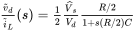
In designing the controller, the output of ![]() in Figure 6.6b under dynamic conditions has a strong DC component, a second harmonic frequency component
in Figure 6.6b under dynamic conditions has a strong DC component, a second harmonic frequency component ![]() , and a low-frequency (less than 15 Hz) perturbation term:
, and a low-frequency (less than 15 Hz) perturbation term:
Multiplying the reference current peak in Equation (6B.1) with ![]() , the inductor current is
, the inductor current is
In the circuit of Figure 6.2, assuming that the voltage drop across ![]() is negligible,
is negligible,
Substituting into Equation (6B.3) ![]() and the inductor current from Equation (6B.2),
and the inductor current from Equation (6B.2),
Noting that ![]() and neglecting the product of
and neglecting the product of ![]() and
and ![]() ,
,
Equating the perturbation frequency terms on the two sides of the above equation,
Recognizing that in the PFC of Figure 6.1a, ![]() . Therefore in Equation (6B.6),
. Therefore in Equation (6B.6),
In the PFC output stage of Figure 6.1a, the voltage and the current are related as
Substituting Equation (6B.8) into Equation (6B.7),