
13
THYRISTOR CONVERTERS
13.1 INTRODUCTION
Historically, thyristor converters were used to perform tasks that are now performed by switch-mode converters, discussed in previous chapters. Thyristor converters are now typically used in utility applications at very high power levels. In this chapter, we will examine the operating principles of thyristor-based converters.
13.2 THYRISTORS (SCRs)
A thyristor is a device that can be considered a controlled diode. Like diodes, they are available in very large voltage and current ratings, making them attractive for use in applications at very high power levels.
Thyristors, shown by their symbol in Figure 13.1a, are sometimes referred to by their trade name of silicon controlled rectifiers (SCRs). These are 4-layer (p-n-p-n) devices, as shown in Figure 13.1b. When a reverse (![]() ) voltage is applied, the flow of current is blocked by the junctions pn1 and pn3. When a forward (
) voltage is applied, the flow of current is blocked by the junctions pn1 and pn3. When a forward (![]() ) polarity voltage is applied, and the gate terminal is open, the flow of current is blocked by the junction pn2, and the thyristor is considered to be in a forward-blocking state. In this forward-blocking state, applying a small positive voltage to the gate with respect to the cathode for a short interval supplies a pulse of gate current
) polarity voltage is applied, and the gate terminal is open, the flow of current is blocked by the junction pn2, and the thyristor is considered to be in a forward-blocking state. In this forward-blocking state, applying a small positive voltage to the gate with respect to the cathode for a short interval supplies a pulse of gate current ![]() that latches the thyristor in its on state, and subsequently, the gate-current pulse can be removed.
that latches the thyristor in its on state, and subsequently, the gate-current pulse can be removed.

FIGURE 13.1 Thyristors.
13.2.1 Primitive Thyristor Rectifier Circuits
The behavior of thyristors is illustrated by means of a simple circuit with a resistive load in Figure 13.2a. At ![]() , the positive half-cycle of the input voltage begins, beyond which a forward voltage appears across the thyristor (anode A is positive with respect to cathode K), and if the thyristor were a diode, a current would begin to flow in this circuit. This instant we will refer to as the instant of natural conduction. With the thyristor in a forward-blocking state, the start of conduction can be controlled (delayed) with respect to the instant of natural conduction, which is
, the positive half-cycle of the input voltage begins, beyond which a forward voltage appears across the thyristor (anode A is positive with respect to cathode K), and if the thyristor were a diode, a current would begin to flow in this circuit. This instant we will refer to as the instant of natural conduction. With the thyristor in a forward-blocking state, the start of conduction can be controlled (delayed) with respect to the instant of natural conduction, which is ![]() in this circuit, by a delay angle
in this circuit, by a delay angle ![]() at which instant the gate-current pulse is applied. Once in the conducting state, the thyristor behaves like a diode with a very small voltage drop of the order of 1 to 2 volts across it (we will idealize it as zero), and the load voltage
at which instant the gate-current pulse is applied. Once in the conducting state, the thyristor behaves like a diode with a very small voltage drop of the order of 1 to 2 volts across it (we will idealize it as zero), and the load voltage ![]() equals
equals ![]() in Figure 13.2b, where
in Figure 13.2b, where ![]() is indicated by the darker waveform. The current equals
is indicated by the darker waveform. The current equals ![]() , as shown in Figure 13.2b.
, as shown in Figure 13.2b.

FIGURE 13.2 A simple thyristor circuit with a resistive load.
The current declines to zero at ![]() , and since it cannot reverse through the thyristor, it stays zero during the negative half-cycle of the voltage waveform, as shown in Figure 13.2b. The current through the thyristor stays zero until the gate pulse is applied in the next cycle of the voltage waveform. The average value
, and since it cannot reverse through the thyristor, it stays zero during the negative half-cycle of the voltage waveform, as shown in Figure 13.2b. The current through the thyristor stays zero until the gate pulse is applied in the next cycle of the voltage waveform. The average value ![]() of the load voltage is indicated by the dotted line in Figure 13.2b. This average value can be calculated analytically from the
of the load voltage is indicated by the dotted line in Figure 13.2b. This average value can be calculated analytically from the ![]() waveform in Figure 13.2b as
waveform in Figure 13.2b as
 (13.1)
where ![]() is the peak of the input AC voltage. From Equation 13.1, it is clear that we can control the average load voltage by controlling the delay angle
is the peak of the input AC voltage. From Equation 13.1, it is clear that we can control the average load voltage by controlling the delay angle ![]() ; this was not possible in the diode-rectifier circuits of Chapter 5.
; this was not possible in the diode-rectifier circuits of Chapter 5.
To consider the influence of inductance in series, consider the primitive circuit of Figure 13.3a. The associated waveforms in Figure 13.3b show that due to the inductor, the current builds up slowly and comes to zero some time in the negative half-cycle of the input voltage. The current through the thyristor cannot reverse and remains zero for the remainder of the input voltage cycle. This principle can be extended to practical circuits discussed below.

FIGURE 13.3 Thyristor circuit with a resistive load and a series inductance.
13.3 SINGLE-PHASE, PHASE-CONTROLLED THYRISTOR CONVERTERS
Figure 13.4a shows a commonly used full-bridge phase-controlled converter for controlled rectification of the single-phase utility voltage. To understand the operating principle, it is redrawn in Figure 13.4b, where the AC-side inductance ![]() is ignored, and the DC-side load is represented as drawing a constant current
is ignored, and the DC-side load is represented as drawing a constant current ![]() . The waveforms are shown in Figure 13.5.
. The waveforms are shown in Figure 13.5.

FIGURE 13.4 Full-bridge, single-phase thyristor converter

FIGURE 13.5 Single-phase thyristor converter waveforms.
Thyristors (1, 2) and (3, 4) are treated as two pairs, where each thyristor pair is supplied gate pulses delayed by an angle ![]() with respect to the instant of natural conduction at
with respect to the instant of natural conduction at ![]() for thyristors (1, 2) and at
for thyristors (1, 2) and at ![]() for 3 and 4, as shown in Figure 13.5.
for 3 and 4, as shown in Figure 13.5.
In the positive half-cycle of the input voltage, thyristors 1 and 2 are forward-blocking until they are gated at ![]() when they immediately begin to conduct
when they immediately begin to conduct ![]() (because
(because ![]() is assumed to be zero), and thyristors 3 and 4 become reverse-blocking. In this state,
is assumed to be zero), and thyristors 3 and 4 become reverse-blocking. In this state,
These relationships hold true until ![]() in the negative half-cycle of the input voltage when thyristors 3 and 4 are gated and begin conducting
in the negative half-cycle of the input voltage when thyristors 3 and 4 are gated and begin conducting ![]() . In this state,
. In this state,
which holds true for one half-cycle until the next half-cycle begins with the gating of thyristors 1 and 2.
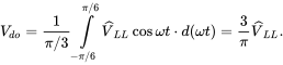
The average value ![]() of the voltage across the DC side of the converter can be obtained by averaging the
of the voltage across the DC side of the converter can be obtained by averaging the ![]() waveform in Figure 13.5 over only one half-cycle (by symmetry) during
waveform in Figure 13.5 over only one half-cycle (by symmetry) during ![]() :
:
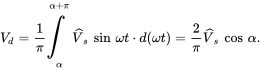 (13.4)
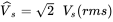
On the AC side, the input current ![]() waveform is shifted by an angle
waveform is shifted by an angle ![]() with respect to the input voltage, as shown in Figure 13.5, and the fundamental-frequency component
with respect to the input voltage, as shown in Figure 13.5, and the fundamental-frequency component ![]() has a peak value of
has a peak value of
In terms of voltage and current peak values, the power drawn from the AC side is
Assuming no power loss in the thyristor converter, the input power equals the power to the DC side of the converter. Using Equations 13.4 and 13.5, we can reconfirm the following relationship:
In this converter, the current is unidirectional, but the DC-side voltage can be controlled and can be of either polarity. Therefore, the power flow can be controlled by the delay angle ![]() ; increasing it toward
; increasing it toward ![]() reduces the average DC-side voltage
reduces the average DC-side voltage ![]() while simultaneously shifting the input current
while simultaneously shifting the input current ![]() waveform farther away with respect to the input voltage waveform. The DC voltage as a function of
waveform farther away with respect to the input voltage waveform. The DC voltage as a function of ![]() is plotted in Figure 13.6a, and the corresponding power direction is shown in Figure 13.6b. The waveforms in Figure 13.5 show that for the delay angle
is plotted in Figure 13.6a, and the corresponding power direction is shown in Figure 13.6b. The waveforms in Figure 13.5 show that for the delay angle ![]() in a range from
in a range from ![]() to
to ![]() ,
, ![]() has a positive value, as also plotted in Figures 13.6a and 13.6b, and the converter operates as a rectifier, with power flowing from the AC side to the DC side.
has a positive value, as also plotted in Figures 13.6a and 13.6b, and the converter operates as a rectifier, with power flowing from the AC side to the DC side.
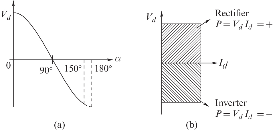
FIGURE 13.6 Effect of the delay angle  .
.
Delaying the gating pulse such that ![]() is greater than
is greater than ![]() in Figure 13.5 makes
in Figure 13.5 makes ![]() negative (also confirmed by Equation 13.4), and the converter operates as an inverter, as illustrated in Example 13.1.
negative (also confirmed by Equation 13.4), and the converter operates as an inverter, as illustrated in Example 13.1.
Draw the waveforms for the full-bridge thyristor converter of Figure 13.4b if it’s operating in an inverter mode with the delay angle ![]() equal to
equal to ![]() .
.
Solution Since ![]() now equals
now equals ![]() , in comparison to Figure 13.5, the
, in comparison to Figure 13.5, the ![]() waveform is shifted by
waveform is shifted by ![]() with respect to
with respect to ![]() waveform as shown in Figure 13.7.
waveform as shown in Figure 13.7.

FIGURE 13.7 Single-phase thyristor converter in an inverter mode with  .
.
In the inverter mode, as shown in Figure 13.6b, power flows from the DC side to the AC side. In practical circuits with inductance in series on the AC side, the upper limit on ![]() in the inverter mode is less than
in the inverter mode is less than ![]() , for example,
, for example, ![]() , as shown in Figure 13.6a, to avoid a phenomenon known as the commutation failure, where the current fails to commutate fully from the conducting thyristor pair to the next pair, prior to the instant beyond which the conducting pair keeps on conducting for another half-cycle. This commutation-failure phenomenon is described in greater detail in [1].
, as shown in Figure 13.6a, to avoid a phenomenon known as the commutation failure, where the current fails to commutate fully from the conducting thyristor pair to the next pair, prior to the instant beyond which the conducting pair keeps on conducting for another half-cycle. This commutation-failure phenomenon is described in greater detail in [1].
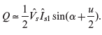
13.3.1 Current Harmonics and Reactive Power Requirement
As can be seen from the AC-side current waveform ![]() in Figure 13.5, the current is rectangular, and the fundamental-frequency waveform is drawn dotted, whose amplitude
in Figure 13.5, the current is rectangular, and the fundamental-frequency waveform is drawn dotted, whose amplitude ![]() is given in Equation 13.5. From Fourier analysis, the harmonics
is given in Equation 13.5. From Fourier analysis, the harmonics ![]() of
of ![]() can be expressed in terms of the fundamental frequency component as
can be expressed in terms of the fundamental frequency component as
As can be observed from Figure 13.5, ![]() is displaced with respect to
is displaced with respect to ![]() by the delay angle
by the delay angle ![]() . Therefore, the reactive power drawn by the converter is
. Therefore, the reactive power drawn by the converter is
13.3.2 Effect of  on Current Commutation
Previously, our assumption was that the AC-side inductance ![]() equals zero. Now consider the circuit in Figure 13.8a. In this case, the input current takes a finite amount of time to reverse its direction through the AC-side inductance as the current “commutates” from one thyristor pair to the next.
equals zero. Now consider the circuit in Figure 13.8a. In this case, the input current takes a finite amount of time to reverse its direction through the AC-side inductance as the current “commutates” from one thyristor pair to the next.

FIGURE 13.8 Effect of  on current commutation.
From basic principles, we know that changing the current through the inductor ![]() in the circuit of Figure 13.8a requires a finite amount of volt-seconds. The DC side is still represented by a DC current
in the circuit of Figure 13.8a requires a finite amount of volt-seconds. The DC side is still represented by a DC current ![]() . The waveforms are shown in Figure 13.8b, where thyristors 3 and 4 are conducting prior to
. The waveforms are shown in Figure 13.8b, where thyristors 3 and 4 are conducting prior to ![]() , and
, and ![]() .
.
At ![]() , thyristors 1 and 2, which have been forward blocking, are gated, and hence they immediately begin to conduct. However, the current through them doesn’t jump instantaneously as in the case of
, thyristors 1 and 2, which have been forward blocking, are gated, and hence they immediately begin to conduct. However, the current through them doesn’t jump instantaneously as in the case of ![]() where
where ![]() instantaneously changed from
instantaneously changed from ![]() to
to ![]() . With a finite
. With a finite ![]() , during a short interval called the commutation interval u, all thyristors conduct, thus resulting in
, during a short interval called the commutation interval u, all thyristors conduct, thus resulting in ![]() and applying
and applying ![]() across
across ![]() . To correspond to Figure 13.8b, where waveforms are plotted with respect to
. To correspond to Figure 13.8b, where waveforms are plotted with respect to ![]() , we will calculate the commutation voltage integral in volt-radians rather than in volt-seconds. The volt-radians needed to change the inductor current from
, we will calculate the commutation voltage integral in volt-radians rather than in volt-seconds. The volt-radians needed to change the inductor current from ![]() to
to ![]() can be calculated by integrating the inductor voltage
can be calculated by integrating the inductor voltage ![]() from
from ![]() to
to ![]() , as follows:
, as follows:
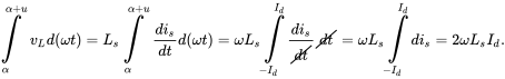 (13.10)
The above volt-radians are “lost” from the integral of the DC-side voltage waveform in Figure 13.8b every half-cycle, as shown by the shaded area ![]() in Figure 13.8b. Therefore, dividing the volt-radians in Equation 13.10 by the
in Figure 13.8b. Therefore, dividing the volt-radians in Equation 13.10 by the ![]() radians each half-cycle, the voltage drop in the DC-side voltage is
radians each half-cycle, the voltage drop in the DC-side voltage is
This voltage is lost from the DC-side average voltage in the presence of ![]() . Therefore, the average voltage is smaller than that in Equation 13.4:
. Therefore, the average voltage is smaller than that in Equation 13.4:
We should note that the voltage drop in the presence of ![]() doesn’t mean a power loss in
doesn’t mean a power loss in ![]() ; it simply means a reduction in the voltage available on the DC side.
; it simply means a reduction in the voltage available on the DC side.
Example 13.2
In a single-phase thyristor converter of Figure 13.8a including ![]() , derive the expression for the commutation angle
, derive the expression for the commutation angle ![]() , and (b) calculate it if
, and (b) calculate it if ![]() ,
, ![]() ,
, ![]() , and
, and ![]() . Frequency
. Frequency ![]() .
.
Solution
- From Figure 13.8a, in Equation 13.10 during the commutation interval,
 . Therefore, substituting
  for
for  in Equation 13.10,

or
 (13.13)
- Substituting the given values in Equation 13.13, where
 , the commutation angle
  .
.
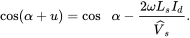
Assuming a linear increase/decrease in thyristor currents in Figure 13.8, the fundamental frequency component ![]() shown dotted in Figure 13.8b lags the voltage
shown dotted in Figure 13.8b lags the voltage ![]() by an angle
by an angle ![]() :
:
where the approximately-equal sign is due to the assumption of linear increase/decrease in thyristor currents. Therefore, the reactive power drawn by the converter is
 (13.15)
13.4 THREE-PHASE, FULL-BRIDGE THYRISTOR CONVERTERS
Three-phase full-bridge converters use six thyristors, as shown in Figure 13.9a. A simplified converter for initial analysis is shown in Figure 13.9b, where the AC-side inductance ![]() is assumed zero, thyristors are divided into a top group and a bottom group, similar to the three-phase diode rectifiers, and the DC side is represented by a current source
is assumed zero, thyristors are divided into a top group and a bottom group, similar to the three-phase diode rectifiers, and the DC side is represented by a current source ![]() .
.

FIGURE 13.9 Three-phase full-bridge thyristor converter.
The converter waveforms, where the delay angle ![]() (measured with respect to the instant at which phase voltage waveforms cross each other) is zero, are similar to those in diode rectifiers, discussed in Chapter 5 (see Figures 5.11 and 5.12). The average DC voltage is as calculated in Equation 5.33, where
(measured with respect to the instant at which phase voltage waveforms cross each other) is zero, are similar to those in diode rectifiers, discussed in Chapter 5 (see Figures 5.11 and 5.12). The average DC voltage is as calculated in Equation 5.33, where ![]() is the peak value of the AC input voltage:
is the peak value of the AC input voltage:
 (13.16)
Delaying the gate pulses to the thyristors by an angle ![]() measured with respect to their instants of natural conductions, the waveforms are shown in Figure 13.10 where
measured with respect to their instants of natural conductions, the waveforms are shown in Figure 13.10 where ![]() .
.

FIGURE 13.10 Waveforms with  .
.
In the DC-side output voltage waveforms, the area ![]() corresponds to “volt-radians loss” due to delaying the gate pulses by
corresponds to “volt-radians loss” due to delaying the gate pulses by ![]() every
every ![]() radian. Assuming the time-origin as shown in Figure 13.10 at the instant at which
radian. Assuming the time-origin as shown in Figure 13.10 at the instant at which ![]() and
and ![]() waveforms cross, the line-line voltage
waveforms cross, the line-line voltage ![]() waveform can be expressed as
waveform can be expressed as ![]() . Therefore from Figure 13.10, the drop
. Therefore from Figure 13.10, the drop ![]() in the average DC-side voltage can be calculated as
in the average DC-side voltage can be calculated as
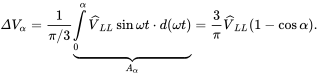 (13.17a)
Using Equations 13.16 and 13.17a, with a finite delay angle ![]() , the DC-side voltage is
, the DC-side voltage is
The phase currents in Figure 13.9a can be expressed as
where ![]() ,
, ![]() , and so on, are the currents in the forward direction through the thyristors. Currents through all three phases are shown in Figure 13.10. These waveforms show that each thyristor conducts for
, and so on, are the currents in the forward direction through the thyristors. Currents through all three phases are shown in Figure 13.10. These waveforms show that each thyristor conducts for ![]() during a fundamental-frequency cycle, and the effect of the delay angle
during a fundamental-frequency cycle, and the effect of the delay angle ![]() is to shift current waveforms by this angle to the right, causing them to lag their input voltages by this angle.
is to shift current waveforms by this angle to the right, causing them to lag their input voltages by this angle.
Similar to single-phase converters, three-phase thyristor converters go into the inverter mode with the delay angle ![]() exceeding
exceeding ![]() . In the inverter mode, the upper limit on
. In the inverter mode, the upper limit on ![]() is less than
is less than ![]() to avoid commutation failure, just like in single-phase converters. Further details on three-phase thyristor converters can be found in [1].
to avoid commutation failure, just like in single-phase converters. Further details on three-phase thyristor converters can be found in [1].
Example 13.3
Three-phase thyristor converter of Figure 13.9b is operating in its inverter mode with ![]() . Draw waveforms similar to Figure 13.10 for this operating condition.
. Draw waveforms similar to Figure 13.10 for this operating condition.
Solution These waveforms for ![]() in the inverter mode are shown in Figure 13.11.
in the inverter mode are shown in Figure 13.11.
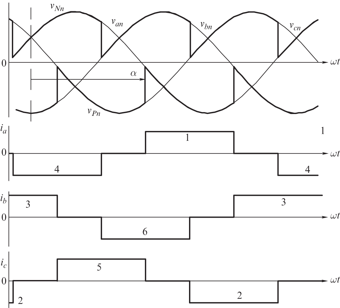
FIGURE 13.11 Waveforms in the inverter mode.
13.4.1⋓Current Harmonics and Reactive Power Requirement
As can be seen from the AC-side current ![]() , for example, in Figure 13.10, the current has a rectangular waveform, and the fundamental-frequency component, from Fourier analysis, has an amplitude
, for example, in Figure 13.10, the current has a rectangular waveform, and the fundamental-frequency component, from Fourier analysis, has an amplitude ![]() :
:
The harmonics ![]() of
of ![]() can be expressed in terms of the fundamental frequency component as
can be expressed in terms of the fundamental frequency component as
In Figure 13.10, ![]() is displaced with respect to
is displaced with respect to ![]() by the delay angle
by the delay angle ![]() . Therefore, the reactive power drawn by the three-phase converter is
. Therefore, the reactive power drawn by the three-phase converter is
13.4.2 Effect of
Unlike in the previous section, due to the presence of ![]() , it takes a finite commutation interval
, it takes a finite commutation interval ![]() for the current to commutate from one thyristor to the next, for example from thyristor 5 connected to phase c to the thyristor 1 connected to phase a. The sub-circuit under discussion during the commutation interval is shown in Figure 13.12a.
for the current to commutate from one thyristor to the next, for example from thyristor 5 connected to phase c to the thyristor 1 connected to phase a. The sub-circuit under discussion during the commutation interval is shown in Figure 13.12a.

FIGURE 13.12 Commutation of current from thyristor 5 to thyristor 1.
During the commutation interval ![]() , from
, from ![]() to
to ![]() , both thyristors are conducting as the current
, both thyristors are conducting as the current ![]() tries to commutate from 5 to 1, and as derived in Example 13.4, the voltage
tries to commutate from 5 to 1, and as derived in Example 13.4, the voltage ![]() is the average of the two-phase voltages:
is the average of the two-phase voltages:
which is shown in Figure 13.12b. As a consequence, the resulting voltage waveforms are shown in Figure 13.13, where such a commutation takes place every ![]() . Considering Figure 13.12a during the commutation interval,
. Considering Figure 13.12a during the commutation interval, ![]() is reduced due to the voltage drop across the inductance in series with thyristor 1 to which the current is commutating from
is reduced due to the voltage drop across the inductance in series with thyristor 1 to which the current is commutating from ![]() to
to ![]() . Using the procedure in Equation 13.10 for single-phase converters, the area
. Using the procedure in Equation 13.10 for single-phase converters, the area ![]() (in volt-radians) in Figure 13.13 can be calculated as
(in volt-radians) in Figure 13.13 can be calculated as

FIGURE 13.13 Waveforms with  .
.
Since such a commutation takes place every ![]() radians, the average DC output voltage is reduced by the area
radians, the average DC output voltage is reduced by the area ![]() divided by
divided by ![]() radians. Making use of Equation 13.23, the drop in the average DC-side voltage is
radians. Making use of Equation 13.23, the drop in the average DC-side voltage is
Therefore, the DC-side output voltage can be written as
Substituting results from Equations 13.16, 13.17, and 13.24 into Equation 13.25,
Example 13.4
In a three-phase thyristor converter of Figure 13.9a including ![]() , (a) derive the expression for the commutation angle
, (a) derive the expression for the commutation angle ![]() , and (b) calculate it if
, and (b) calculate it if ![]() ,
, ![]() ,
, ![]() , and
, and ![]() .
.
Solution a. In the sub-circuit of Figure 13.12a when both thyristors are conducting, applying Kirchhoff’s current law at point ![]() ,
,
Assuming ![]() to be constant, taking the time derivatives of both sides of Equation 13.20 results in
to be constant, taking the time derivatives of both sides of Equation 13.20 results in
or
Therefore, in Figure 13.12a,
Also,
Adding Equations 13.30 and 13.31 and making use of Equation 13.29,
Substituting the expression for ![]() from Equation 13.32 into Equation 13.30,
from Equation 13.32 into Equation 13.30,
In Equation 13.33, ![]() is the line-line voltage, and assuming the time-origin in Figure 13.13 at the intersection of the phase-a and phase-c voltages, the voltage drop
is the line-line voltage, and assuming the time-origin in Figure 13.13 at the intersection of the phase-a and phase-c voltages, the voltage drop ![]() in Equation 13.33 can be written as
in Equation 13.33 can be written as
Using Equation 13.34 into Equation 13.23,
and therefore,
from which the commutation interval ![]() can be calculated.
can be calculated.
b. Substituting the given values in Equation 13.36, the commutation interval ![]() is
is ![]() .
.
Similar to single-phase converters, assuming a linear increase/decrease in thyristor currents in Figure 13.12b, the fundamental frequency component ![]() in Figure 13.13 lags the voltage
in Figure 13.13 lags the voltage ![]() by
by
where the approximately-equal sign is due to assuming a linear increase/decrease in thyristor currents.
13.5 CURRENT-LINK SYSTEMS
Thyristors are available in very large current and voltage ratings of several kilo-amperes and several kilovolts that can be connected in series. In addition, thyristor converters can block voltages of both polarities but conduct current only in the forward direction. This capability has led to the interface realized by thyristor-converters with a DC-current link in the middle, as shown in Figure 13.14.

FIGURE 13.14 Block diagram of current-link systems.
Unlike in voltage-link systems, the transfer of power in current-link systems can be reversed in direction by reversing the voltage polarity of the DC link. This structure is used at very high power levels, in excess of a thousand megawatts, for example, in high-voltage DC (HVDC) transmission systems.
Thyristors in these two converters shown in Figure 13.14 are connected to allow the flow of current in the DC link by thyristors in converter 1 pointing up, and the thyristors in converter 2 connected to point downward. In Figure 13.14, subscripts 1 and 2 refer to systems 1 and 2 and ![]() is the resistance of the DC link that includes the DC transmission line. Assuming each converter is a six-pulse thyristor converter, as discussed previously,
is the resistance of the DC link that includes the DC transmission line. Assuming each converter is a six-pulse thyristor converter, as discussed previously,
By controlling the delay angles ![]() and
and ![]() in a range of
in a range of ![]() to
to ![]() (practically, this value is limited to approximately
(practically, this value is limited to approximately ![]() ), the average voltage and the average current in the system of Figure 13.14 can be controlled, where current flow through the DC link can be expressed as
), the average voltage and the average current in the system of Figure 13.14 can be controlled, where current flow through the DC link can be expressed as
Since the DC-link resistance ![]() is generally very small,
is generally very small, ![]() and
and ![]() are very close in magnitude and opposite in value. For example, for the power flow from system 1 to system 2,
are very close in magnitude and opposite in value. For example, for the power flow from system 1 to system 2, ![]() is made negative by controlling
is made negative by controlling ![]() such that converter 2 operates as an inverter and establishes the voltage of the DC link. Converter 1 is operated as a rectifier, with a positive value of
such that converter 2 operates as an inverter and establishes the voltage of the DC link. Converter 1 is operated as a rectifier, with a positive value of ![]() , at a delay angle
, at a delay angle ![]() such that it controls the current in the DC link. The converse is true for these two converters if the power is to flow from system 2 to system 1.
such that it controls the current in the DC link. The converse is true for these two converters if the power is to flow from system 2 to system 1.
The above discussion of current-link systems shows the operating principle behind HVDC transmission systems discussed in the next chapter, where using transformers, six-pulse thyristor converters are connected in series on the DC side and in parallel on the AC side to yield a higher effective pulse number.
REFERENCE
- 1. N. Mohan, T.M. Undeland, and W.P. Robbins, Power Electronics: Converters, Applications and Design, 3rd Edition (New York: John Wiley & Sons, 2003).
PROBLEMS
Single-Phase Thyristor Converters
In a single-phase thyristor converter, ![]() at
at ![]() , and
, and ![]() . The delay angle
. The delay angle ![]() . This converter is supplying
. This converter is supplying ![]() of power. The DC-side current
of power. The DC-side current ![]() can be assumed purely DC.
can be assumed purely DC.
- 13.1 Calculate the commutation angle
 .
. - 13.2 Draw the waveforms for the converter variables
 ,
,  and
and  .
. - 13.3 Assuming that the currents through the thyristors increase/decrease linearly during commutations, calculate the reactive power drawn by the converter.
Three-Phase Thyristor Converters
In a three-phase thyristor converter, ![]() at
at ![]() , and
, and ![]() . The delay angle
. The delay angle ![]() . This converter is supplying
. This converter is supplying ![]() of power. The DC-side current
of power. The DC-side current ![]() can be assumed purely DC.
can be assumed purely DC.
- 13.4 Calculate the commutation angle
 .
. - 13.4 Draw the waveforms for the converter variables: phase voltages, phase currents,
 ,
,  and
and  .
. - 13.6 Assuming that the currents through the thyristors increase/decrease linearly during commutations, calculate the reactive power drawn by the converter.
- 13.7 In a three-phase thyristor converter, assume the commutation angle to be zero. Also, assume a given AC-side voltage
 and that the DC-side current
  is kept constant in magnitude. Plot the reactive power
  drawn by the converter in terms of
  ,
,  , as a function of the delay angle
  . Explain why it is desirable to operate the converter close to
  in the rectifier mode and close to
  in the inverter mode.
Current-Link System
- 13.8 In the block diagram of Figure 13.14, for both three-phase converters,
 . The DC-side current is
  . Converter 2 operating as an inverter establishes the DC-link voltage such that
  .
.  . The drop in DC voltage due to commutation overlap in each converter is
  . In DC steady state, calculate the following angles:
  ,
,  ,
,  and
and  .
. - 13.9 In Problem 13.8, calculate the reactive power drawn by each converter. Assume that the currents through the thyristors increase/decrease linearly during commutations.
Simulation Problems
- In a single-phase thyristor converter, the input voltage is
 at 60 Hz frequency. The AC-side inductance is 1.2 mH, and on the DC side the load has an inductance of 20 mH in series with a resistance of 5 Ω.
- Obtain the
 waveforms.
 - Obtain the
 waveforms.
 - From the plots, obtain the commutation interval
 .
. - By means of Fourier analysis of
 , calculate its harmonic components as a ratio of
  .
. - Calculate
 , %THD in the input current, the input displacement power factor, and the input power factor.