
7
FPGA SoC Hardware Design and Verification Flow
In this chapter, we will delve into implementing the SoC hardware of the Electronic Trading System (ETS), for which we developed the architecture in Chapter 6, What Goes Where in a High-Speed SoC Design. We will first go through the process of installing the Xilinx Vivado tools on a Linux Virtual Machine (VM). Then, we will define the SoC hardware microarchitecture to implement using the Xilinx Vivado tools. This chapter is purely hands-on, where you will build a simple but complete hardware SoC for a Xilinx FPGA. You will be guided at every step of the SoC hardware design, from the concept to the FPGA image generation. This will also cover hardware verification aspects, such as using the available RTL simulation tools to check the design and look for potential hardware issues.
In this chapter, we’re going to cover the following main topics:
- Installing the Xilinx Vivado tools on a Linux VM
- Developing the SoC hardware microarchitecture
- Design capture of an FPGA SoC hardware subsystem
- Understanding the design constraints and PPA
- Verifying the FPGA SoC design using RTL simulation
- Implementing the FPGA SoC design and FPGA hardware image generation
Technical requirements
The GitHub repo for this title can be found here: https://github.com/PacktPublishing/Architecting-and-Building-High-Speed-SoCs.
Code in Action videos for this chapter: http://bit.ly/3NRZCkU.
Installing the Vivado tools on a Linux VM
The Xilinx Vivado tools aren’t supported on Windows 10.0 Home edition, so if you are using your home computer with this version installed on it, you won’t be able to follow the practical parts of this book. Only Windows 10.0 Enterprise and Professional editions are officially supported by the Vivado tools. However, there are many Linux-based Operating Systems (OSes) that Xilinx officially supports.
One potential solution to build a complete learning environment using your home machine is to install the Vivado tools on a supported Linux version, such as Ubuntu, which you can run as a VM by using the Oracle VirtualBox hypervisor to host it.
The Vivado tools are officially supported on the following OSes:
- Windows: Windows Enterprise and Professional 10.0
- RedHat Linux: RHEL7, RHEL8, and CentOS 8
- SUSE Linux: EL 12.4, and SUSE EL 15.2
- Ubuntu: From 16.04.5 LTS up to 20.04.1 LTS
Information
For the full list of supported OS versions and revisions, please check out https://www.xilinx.com/products/design-tools/vivado/vivado-ml.html#operating-system.
For our practical design examples and to achieve the learning objectives, we can use a good specification home machine running Windows 10.0 Home edition as a learning platform. We will install Oracle VirtualBox on it, and then we will build a VM with Ubuntu 20.04 LTS Linux as a guest OS.
A good machine that we can use for the examples in this book should have at least the following hardware specification:
- Processor: Intel(R) Core(TM) i5-10400 CPU @ 2.90 GHz
- Installed RAM: 16.00 GB
- System type: A 64-bit OS and an x64-based processor
Installing Oracle VirtualBox and the Ubuntu Linux VM
Oracle VirtualBox is a hypervisor that can host the Linux VM. You can download it from https://www.oracle.com/uk/virtualization/technologies/vm/downloads/virtualbox-downloads.html.
You can install VirtualBox by double-clicking on the downloaded install executable – for example, we are using the VirtualBox-6.1.34-150636-Win.exe build.
You also need to download Ubuntu Linux from https://ubuntu.com/#download.
In VirtualBox, we can now proceed to build the Ubuntu VM by following these simple steps:
- Go to Machine and select New, as shown here:

Figure 7.1 – Creating a new VM in VirtualBox
- This will open the following window, where you can name the VM, for example, UbuntuVM, and then specify which guest OS we will be using (Linux and Ubuntu (64-bit)). Click on Next:
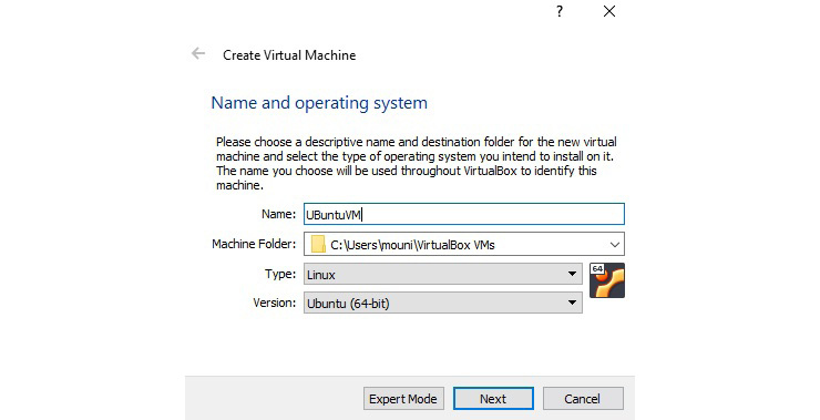
Figure 7.2 – Entering the name and the OS to use
- This will open the following window, where we specify the size of the RAM allocated to the VM. We need at least 5 GB to run the Vivado tools and target the Zynq-7000 SoC FPGAs. Increase the value to something higher than 5 GB, and then click Next.
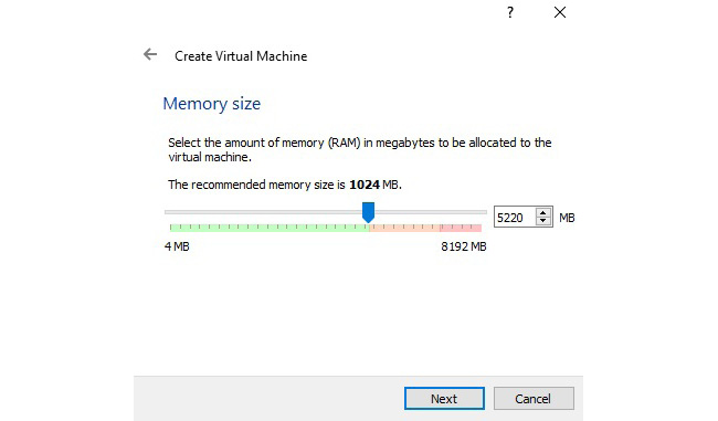
Figure 7.3 – Specifying the memory size of the VM
- Now, we need to create a hard disk for the VM; choose the default and click on Create.
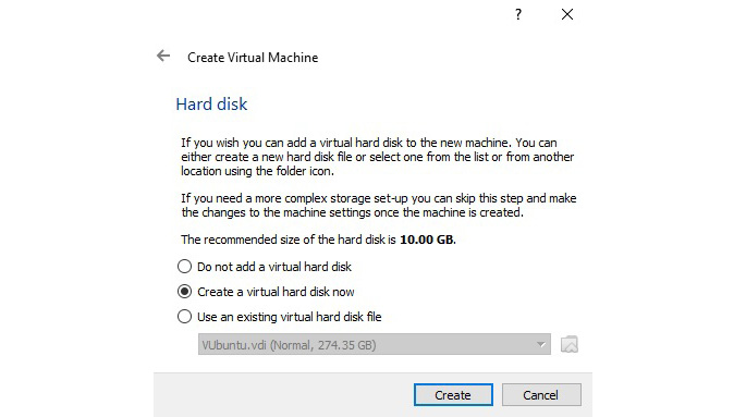
Figure 7.4 – Creating the hard disk for the VM
- This will open the next window for specifying the type of virtual hard disk to create for the VM. Choose the default as shown and click on Next.
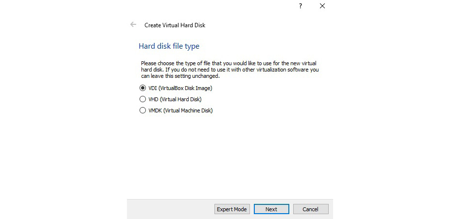
Figure 7.5 – Specifying the virtual hard disk type of the VM
- Now, we need to specify the allocation of the storage of the virtual disk on the physical disk; choose an option from the two and then click on Next.
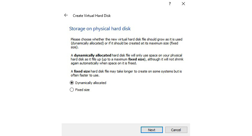
Figure 7.6 – Specifying the virtual hard disk storage allocation type
- Now, we need to specify the size of the virtual hard disk, as shown in the following figure. Choose something around 200 GB if you have spare space on your computer, as we need space for the Vivado tools (50 GB) and space for the installation process. Click on Create.
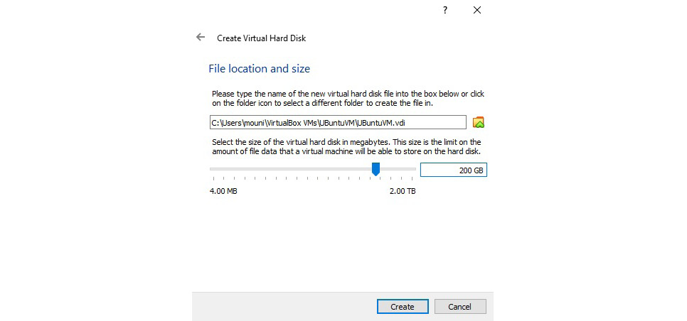
Figure 7.7 – Specifying the size of the virtual hard disk
The VM is now created, as shown in the following figure.
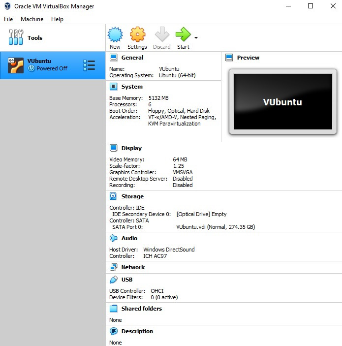
Figure 7.8 – The UbuntuVM VM created in VirtualBox
- To start the VM and install the Ubuntu Linux OS on it, just double-click on it or use the green arrow on the right-hand side. This will open the following window. The first time this VM boots, we need to specify the OS image via the window that opens automatically. Click on the green arrow in the folder icon.
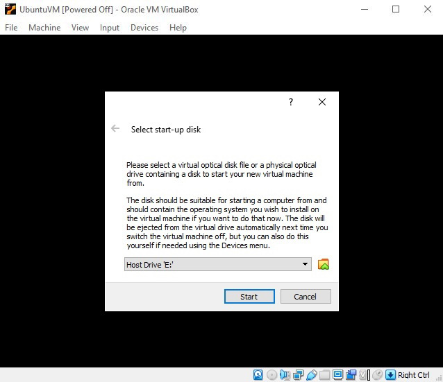
Figure 7.9 – Launching the UbuntuVM VM for the first time from VirtualBox
- The following window will open. Click on the Add sign to specify the path to the Ubuntu Linux ISO file previously downloaded. Browse to the Ubuntu Linux ISO image, and then click on Choose.
Figure 7.10 – Specifying the OS to use with the VM
- This will open the launch window of the Ubuntu VM, as shown here. Click on Start.

Figure 7.11 – Starting the UbuntuVM VM
- In the screen that follows, just click on Enter to install Ubuntu Linux on the VM as the guest OS. Once the Linux OS boots, just follow the instructions to set it up for the first time.
We now have an officially supported OS that can be used for our learning objectives.
Installing Vivado on the Ubuntu Linux VM
From within the Ubuntu Linux VM, download the Xilinx Vivado installer for Linux from https://www.xilinx.com/support/download.html.
To gain access and be able to download Vivado, you will need to register first.
Before starting the installation process of Vivado, we need to make sure that we have all the packages required by Vivado to install and operate correctly on Ubuntu Linux. We found that the following libraries and packages are missing in the default Ubuntu Linux installation and simply need to be added:
- libtinfo5
- libncurses5
- "build-essential", which includes the GNU Compiler Collection
To install the preceding packages, simply use the following command from within a command shell in Ubuntu:
$ sudo apt install libtinfo5Then, for libncurses5, use the following command:
$ sudo apt install libncurses5And for the build-essential package, use the following command:
$ sudo apt update
$ sudo apt install build-essential
$ sudo apt-get install manpages-dev
We should have an Ubuntu Linux build ready to install the Vivado tools.
Now, we need to launch the installer of the Vivado package. From Command Prompt, use cd to go to the download location and change the binary file attribute to be executable:
$ sudo chmod +x Xilinx_Unified_2022.1_0420_0327_Lin64.binThen, launch it using the following:
$ sudo ./Xilinx_Unified_2022.1_0420_0327_Lin64.binThis will start the installation process by first downloading the necessary packages and installing them. This process may take some time, given the size of the Vivado software package, and how long the installation process will last will depend on your internet connection speed. It is typical to leave it overnight, even over a fiber optic internet connection.
Once Vivado has finished installing, we suggest changing the settings of the Vivado IDE source files Text Editor that is enabled by default in Vivado from Sigasi to Vivado. This will avoid an issue using this Text Editor. When launching any command that requires using the preceding text editor selected by default, we noticed on the UbuntuVM Linux VM that it causes Vivado to get stuck when trying to launch the text editor. To change the Text Editor, simply follow these steps:
- Go to Tools.
- Select Settings.
- Select Tool Settings.
- Then, select Text Editor.
- Then, select Syntax Checking.
- Change the value of the Syntax Checking field from Sigasi to Vivado.
- Restart Vivado.
Developing the SoC hardware microarchitecture
In the previous chapter, we defined the SoC architecture and left it to the implementation stage to choose the optimal solution that meets the specification of the low-latency ETS. We also left the exact details of the Electronic Trading Market Protocol (ETMP) to be defined here as close to the implementation stage as possible, just for practical reasons, since this protocol is really defined by the Electronic Trading Market (ETM) organization. We will define a simple protocol that uses UDP as its transport mechanism between the ETM network and the ETS. We have also not defined the exact details of the communication protocol between the software and the hardware PE for sending the requests to filter from the Cortex-A9, processing them by the hardware PE, and posting the results back from the hardware PE to the Cortex-A9. This protocol will be defined here by finding a fast exchange mechanism to be used by the microarchitecture proposal.
The ETS SoC hardware microarchitecture
From the ETS SoC architecture specification, we can draw a proposal SoC hardware microarchitecture that can implement the required low-latency ETS SoC.
Defining the ETS SoC microarchitecture
We need to build the following functionalities in the hardware acceleration PE:
- Listen to the software via a doorbell register for requests to filter the received Ethernet packets on the Ethernet port:
- On receiving the Ethernet packets via its DMA engine, the software prepares a request for acceleration by providing an Acceleration Request Entry (ARE) in the Acceleration Request Queue (ARQ), located in local memory within the Programmable Logic (PL) side of the SoC.
- This request is in a form of an entry that has three fields: the address of the first DMA descriptor, the number of received packets, and an Acceleration Done status field.
- The length of the ARQ circular buffer needs to be computed according to the speed at which the UDP frames are received from the Ethernet port, and the speed at which they are processed by the hardware accelerator PE.
- The Cortex-A9 should never block on a full request circular buffer.
- The software notifies the hardware accelerator engine that there are received Ethernet frames within the memory that need filtering and processing.
- The hardware accelerator engine receives the notification and information from the Cortex-A9 and performs the packet processing of the Ethernet frames that are found to be UDP packets.
- The hardware accelerator populates the urgent buying queue and notifies the trading algorithm task via an interrupt when it finds a matching symbol.
- The hardware accelerator puts the address (pointer) of the DMA descriptor associated with the UDP packets in the DMA Descriptors Recycling Queue (DDRQ) for the DMA Descriptors Recycling Task (DDRT) to recycle them.
- The hardware accelerator populates the urgent selling queue and notifies the trading algorithm task via an interrupt when it finds a matching symbol.
- The hardware accelerator puts the DMA descriptor associated with the UDP packets in the DDRQ for the DDRT to recycle them.
- The hardware accelerator populates the Market Data Queue (MDQ) and sends a notification to the Market Database Manager Task (MDMT) via an interrupt when it finds a matching symbol.
- Once the Ethernet frames have all been inspected, the hardware accelerator notifies the Cortex-A9 via an interrupt that it has processed all the Ethernet frames from the last ones it has been asked to deal with.
- The Cortex-A9 checks the received Ethernet frames for the ones left untreated by the hardware accelerator (non-UDP packets). When it finds some, it consumes them. The Cortex-A9 software can use any scheme to keep track of these among the ones that were accelerated by the hardware PE.
- The Cortex-A9 changes the value of the Ownership field in the DMA descriptors for the Ethernet frames that it dealt with itself.
- The Cortex-A9 notifies the Ethernet drivers or the DDRT to perform any DMA descriptor recycling actions.
From the preceding request-response summary between the Cortex-A9 and the hardware acceleration PE and the SoC architecture specification, we can come up with many low-latency microarchitecture proposals; one of the simplest designs for the implementation is depicted in the following diagram:
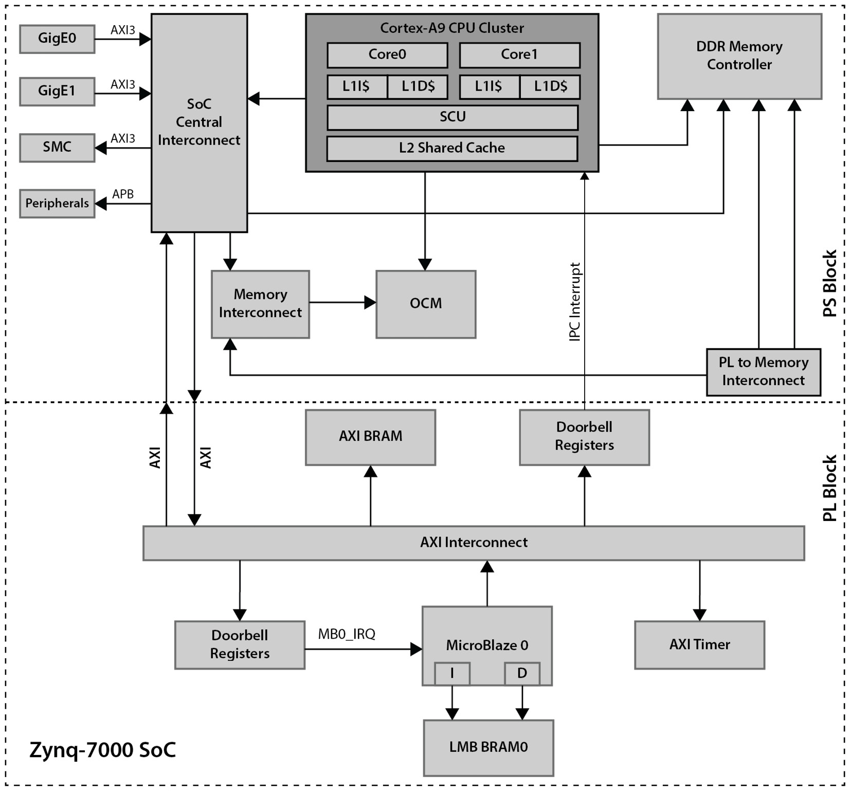
Figure 7.12 – ETS microarchitecture
This microarchitecture is simple to implement, as it uses the MicroBlaze processor as the processing engine of the hardware acceleration. It is well suited for performing packet processing, as it allows the experimentation of many parallel processing algorithms. We can define the best approach that suits the ETS even post-deployment, since this is a real semi-soft algorithm implementation. If we decide to redesign the hardware accelerator as Multiple Data Multiple Engines (MDMEs), we can do so by using multiple MicroBlaze processors and dispatching filtering and packet processing work fairly among them. This will require triplicating the Cortex-A9 interfaces listed previously in this subsection. This is also a scalable microarchitecture, meaning that if we judge that we need a higher processing rate, we can then augment the number of MicroBlaze processors, or increase the operating clock frequency (while the FPGA implementation permits), and obviously reimplement the design. We will also need to reconfigure the FPGA as well as reimplement the Cortex-A9 software, but it can all be done, and in the least disruptive manner, if the FPGA still has the necessary resources to implement extra MicroBlaze-based CPUs. If not, this may require designing newer hardware using the next density available FPGA SoC, using the same package from the Zynq-7000 FPGAs. The dispatch model could also operate in a Single Data Multiple Engines (SDMEs) model. In the SDME model, and for a faster match lookup, the Cortex-A9 can request that all the MicroBlaze processors concurrently search for a specific filter match each, but on the same Ethernet packet. This may speed up the filtering by executing fewer branches on the MicroBlaze software but will increase the complexity of all the software. In this compute model, access to shared data should be atomic among the different MicroBlaze processors as the packet filtering becomes more distributed. However, this is perfectly fine as another microarchitecture proposal option, which will then also be retained. We suggest using the MDME dispatch model for the hardware acceleration engine microarchitecture, and we will be implementing the necessary queues and notification mechanisms for it to work in the next chapter, when we start implementing the ETS SoC software.
ETMP definition
We will define a simple ETMP to transport over a UDP packet for the ETM, for both the Market Management (MM) and the Market Data Information (MDI) packets. For the trading TCP/IP, we will leave it until we start developing the Cortex-A9 software in Chapter 8, FPGA SoC Software Design Flow. The ETMP defines a single-length UDP packet payload of 320 bits/40 bytes and has many fields, as defined in the following table:
|
Field |
Length in bits |
Description |
|
Symbol Code (SC) |
32 |
The financial traded product symbol code. Every financial product has a unique code assigned by the ETM when the product is first introduced to the ETM. |
|
Packet Type (PT) |
32 |
States whether this is an MM packet or a Market Data packet: 0b0: Market Data packet 0b1: Management packet |
|
Proposed Volume (PV) |
32 |
The proposed maximum volume for a sell or buy action. Partial proposals of trade can be made by the ETS if interested in the symbol. |
|
Transaction Type (TT) |
32 |
The transaction type associated with this financial product, buying or selling: 0b0: Buying 0b1: Selling |
|
Timestamp (TS) |
64 |
This is the timestamp logging from when the UDP packet left the ETM servers. |
|
Day (D) |
32 |
Encodes the day when the UDP packet was sent. |
|
Month (M) |
32 |
Encodes the month when the UDP packet was sent. |
|
Year (Y) |
32 |
Encodes the year when the UDP packet was sent. |
|
Error Detection Code (EDC) |
32 |
CRC32 computed over all the ETMP packets, excluding itself (over 288 bits) |
Table 7.1 – The ETMP packet format
The Full ETMP UDP packet within the UDP frame is depicted in the following figure:
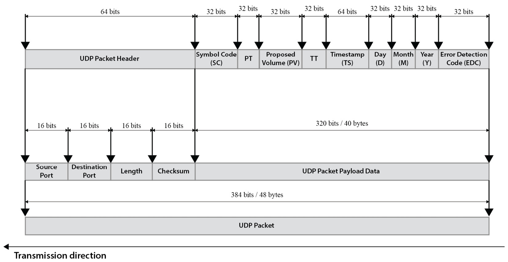
Figure 7.13 – The ETMP packet layout
The UDP header adds another 64 bits of data to the packet, resulting in an ETMP UDP frame of 384 bits/48 bytes, as illustrated in the preceding figure.
There is a possibility to implement a CRC32 calculator in the hardware and connect an instance of it to the MicroBlaze processor, to use for confirming the integrity of the ETMP packet. The alternative solution would be to start with a software function to perform it and deal with it in hardware post-profiling. There are open source implementations of the CRC32 algorithm that we can use, or we can build our own CRC32 function in the software. All of these are options we can decide upon by running a benchmarking exercise on a MicroBlaze-based hardware design, where we profile the software-based CRC32 algorithm implementation and assess its suitability for the low-latency ETS. We will revisit this topic as part of the hardware acceleration in Part 3 of this book.
Design capture of an FPGA SoC hardware subsystem
In this section, we start the building process of the ETS SoC hardware subsystem using the Xilinx Vivado tools. We will start by creating a Vivado project, adding the required subsystem IPs, configuring them, and connecting them to form the SoC using the IP Integrator utility of Vivado. But first, we will create a Vivado project that targets one of the Zynq-7000 SoC demo boards, if we have it at hand; we can then use it to verify the final functionality of the ETS SoC once we have built software for it. Also, any available demo board capable of hosting a Zynq-7000-based SoC design can be used as a target. These design capture steps were introduced in Chapter 2, FPGA Devices and SoC Design Tools, of this book, and we will build upon this information to achieve our current objective.
Creating the Vivado project for the ETS SoC
The first step is to launch the Vivado GUI:
- Start by launching the VirtualBox hypervisor to boot the UbuntuVM Linux VM. If you are using Windows Enterprise or Professional as a host machine, it is still recommended to use a Linux VM for this book’s projects.
- Now, we need to launch the Vivado GUI by using Command Prompt and typing the following:
$ cd <Tools_Install_Directory>/Xilinx/Vivado/2022.1/bin/
$ sudo ./vivado
Replace <Tools_Install_Directory> with the path where you have installed Vivado on your UbuntuVM Linux VM. When prompted for the sudo password, provide the root password you set up when you installed the UbuntuVM Linux VM (assuming you haven’t changed it afterward).
Once Vivado is up and running, we can then create the ETS SoC project by doing either of the following:
- Starting from an existing project template and customizing it to our needs
- Creating the project from scratch, using IP Integrator to add components, and then configuring them
Since we have already gone through the creation of an empty Vivado project in Chapter 2, FPGA Devices and SoC Design Tools, we can now start our design from an existing project template; we will then customize it to our microarchitecture needs and add the necessary IPs, using IP Integrator to implement the hardware PE for the packet filtering tasks. This is a better approach when you are just starting the learning journey of the Xilinx FPGA SoC designs and the hardware design flow. This promotes design reuse, minimizes design bugs, and speeds up the integration process. Let’s begin.
- In the Vivado Quick Start window, click on Open Example Project. This will launch the following menu:
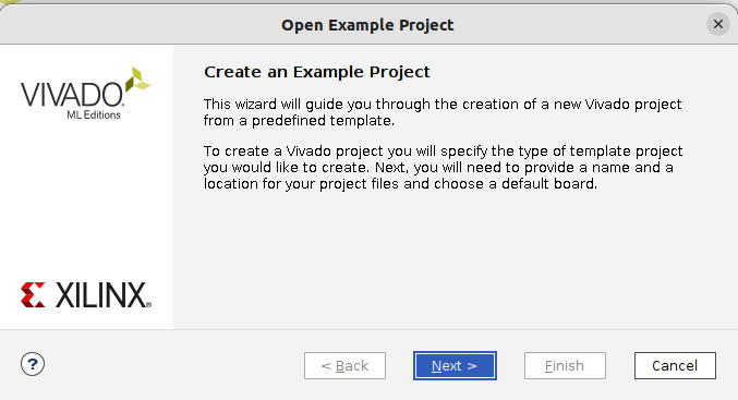
Figure 7.14 – Creating a Vivado project, starting from a predefined template
- Click Next > in the preceding window; this will then open the Select Project Template window. Choose the Zynq-7000 Design Presets option in the Templates section, and then click on Next > once you have read its description.
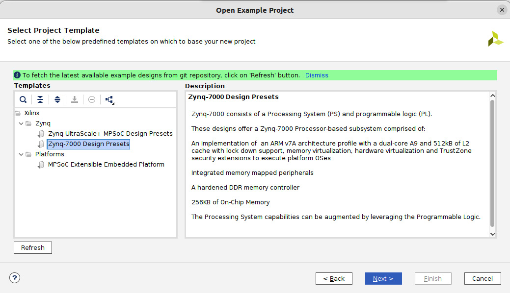
Figure 7.15 – Selecting the predefined template for the ETS SoC
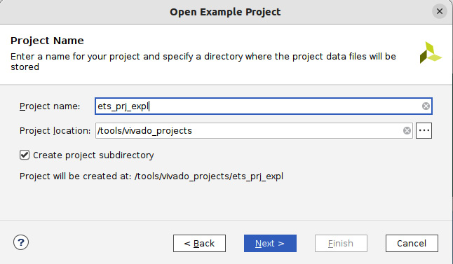
Figure 7.16 – Specifying the ETS SoC project details
- This will open the following window to select a default Xilinx board for this project. Select the board as highlighted in the following screenshot, and then click Next >.
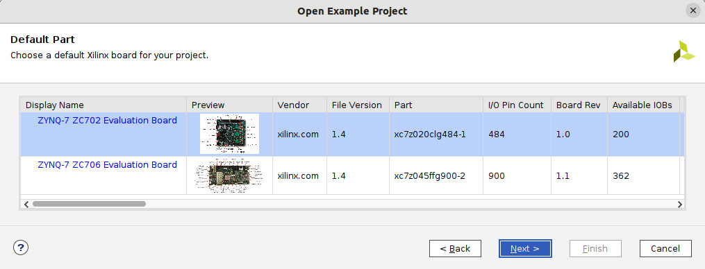
Figure 7.17 – Choosing the default board for the ETS SoC project
- The selection of a design preset can be performed in the following window, as indicated by the following figure, to include both the PS and PL in the ETS SoC. Once selected, click Next >.
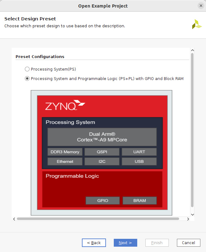
Figure 7.18 – Choosing the design preset for the ETS SoC project
- The last figure in this project template selection is a summary of the chosen preset for the ETS SoC. Click on Finish to open the selected preset project.
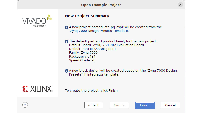
Figure 7.19 – The selected design preset summary for the ETS SoC project
- The ETS SoC project will open, as shown in the following figure. We can now start to explore what is included in it so that we can extend it to meet the ETS SoC hardware microarchitecture needs.
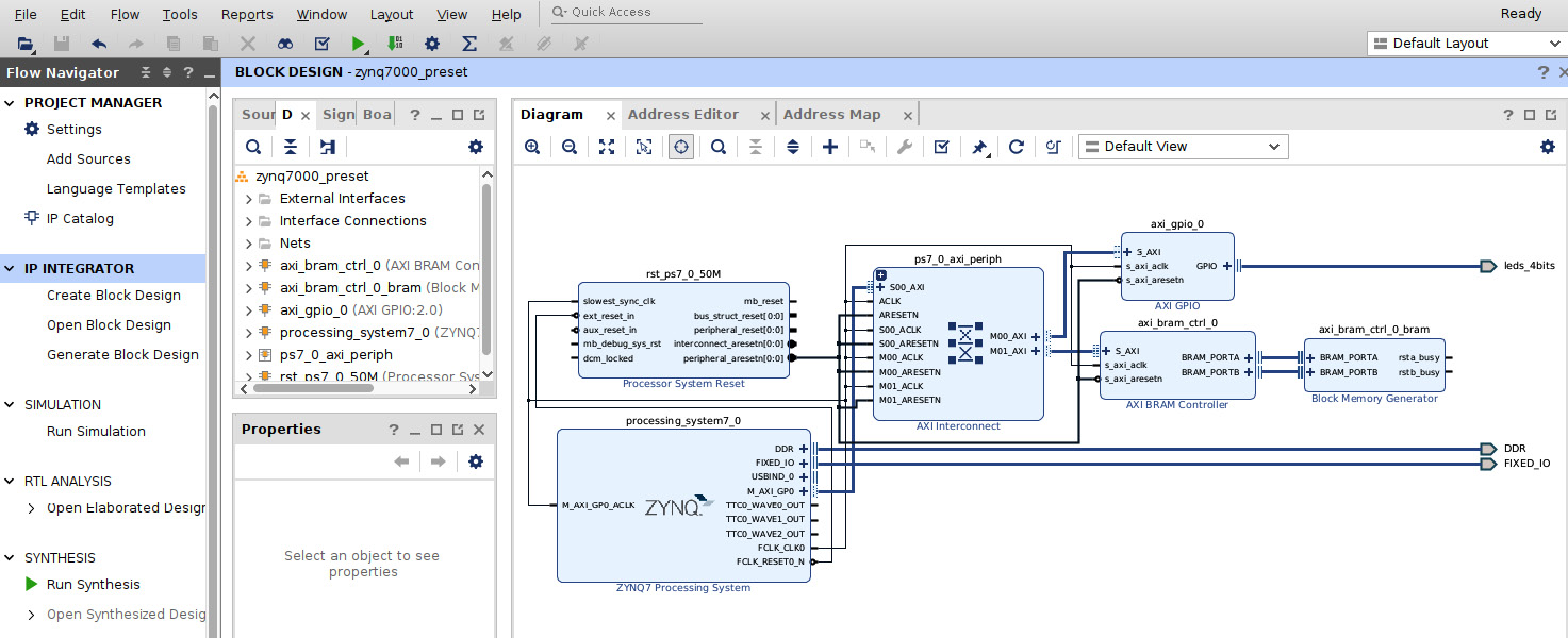
Figure 7.20 – The Vivado ETS SoC project starting preset view
Revisiting the ETS SoC microarchitecture and looking at the preceding Vivado project, we have both the PS and the PL blocks of the FPGA included. In the PL block, we have an AXI BRAM, an AXI GPIO, and an AXI interconnect. We shall keep all these elements, and we shall add the MicroBlaze processor and its required peripherals. For the Cortex-A9 to the MicroBlaze processors' Inter-Process Communication (IPC) interrupt, we will simply use an AXI Interrupt Controller (INTC) IP. The INTC will implement the required doorbell registers, which have the capability to generate software-triggered interrupts. We only need to add these later using IP Integrator, configure them, and then revisit all the preset IPs in the PL block from the template, which should still be valid; if not, correct their settings. Before moving on to the PL block subsystem design task, let’s first make sure the preset configuration of the PS block is in line with our desired features for the ETS SoC microarchitecture. To do so, we can graphically examine the settings and adjust them as needed.
Configuring the PS block for the ETS SoC
In the IP Integrator main window, double-click on the Zynq processing system; this will open the following configuration window. All the parts that are highlighted in green are user-customizable. Let’s proceed to the PS customization task:
- Let’s unselect the peripherals we don’t need for the ETS SoC, such as CAN 0, SD0, and USB 0. To disable these peripherals in the PS, click anywhere in the I/O peripherals.
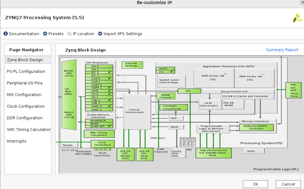
Figure 7.21 – Customizing the peripherals to use in the ETS SoC PS block
- This will open the I/O peripherals selection window. Uncheck the unwanted peripherals, as shown here.
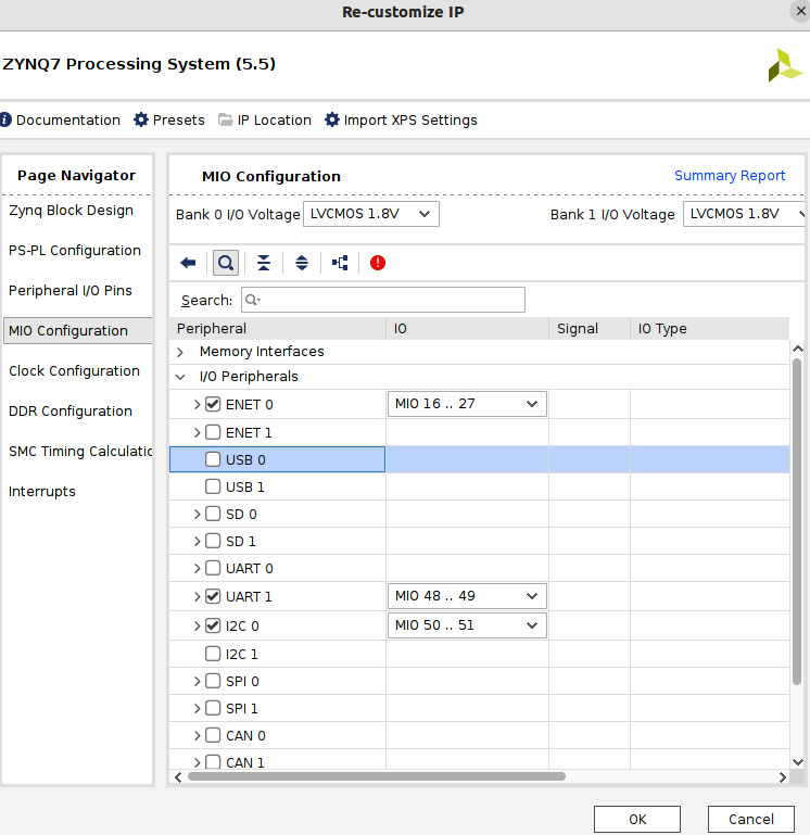
Figure 7.22 – Selecting the peripherals to use in the ETS SoC PS block
- Now, let’s move to the next customization step by selecting the Peripheral I/O Pins row in the Page Navigator pane on the left-hand side of the window; this will open the following view, showing the current assignment of the selected peripherals in the PS block and how they are connected to the external world – that is, via the MIO path and not the EMIO path. We introduced these connectivity options in Chapter 2, FPGA Devices and SoC Design Tools. We should keep the chosen option to match the selected board layout; if we have another alternative board design, we can route them when applicable through the EMIO path via the FPGA PL block.

Figure 7.23 – Customizing the ETS SoC PS peripheral I/O pins
- Select the MIO Configuration row, which will open the MIO Configuration window, showing the selected pins for every I/O of every peripheral selected in the PS block.
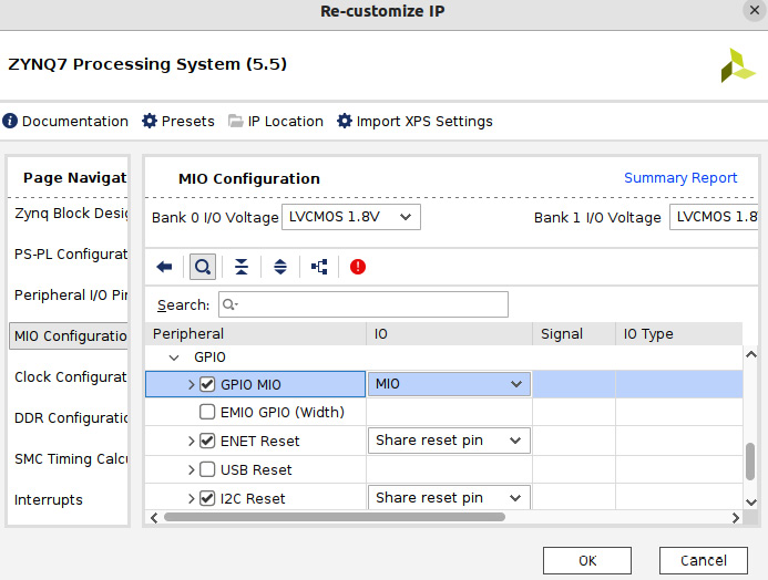
Figure 7.24 – Customizing the ETS SoC PS peripheral I/O pins location
- Select the next row down, which is the Clock Configuration row. We can customize the clocking on the SoC in this window. Set the values as shown in the next figure, setting up the CPU, the DDR, and the PL block interface clocking.
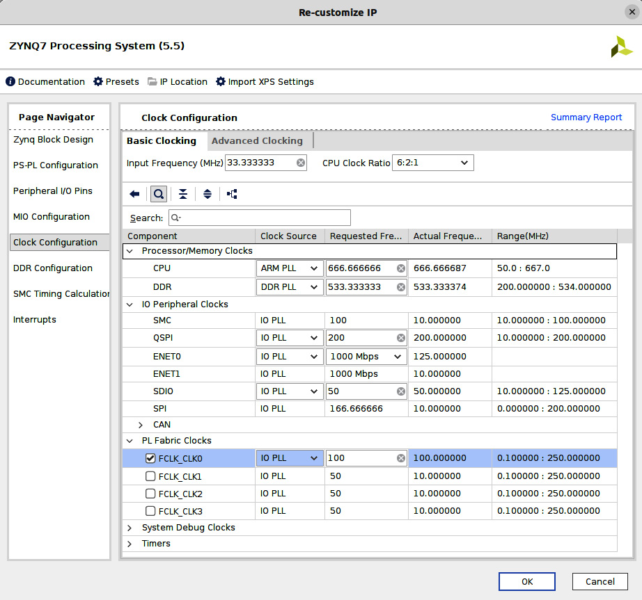
Figure 7.25 – Setting up the PS block IPs clocking
- Select the DDR Configuration row to explore all the available controllers, devices, and board parameters. Leave everything as it is, since it is set for the selected demo board. Anything that needs to be specifically configured for the ETS SoC can be done via the DDR controller registers visible to the software.
- As shown in the following figure, select the Interrupts row to examine the available customization options. Expand the PL-PS Interrupt Ports row, and then add IRQ_F2P[15:0] to enable the 16-bit shared interrupts from the PL. As indicated, these are wired to the Cortex-A9 Generic Interrupt Controller (GIC), and they are connected to the Shared Peripheral Interrupt (SPI) inputs, positioned at [91:84] and [68:61].
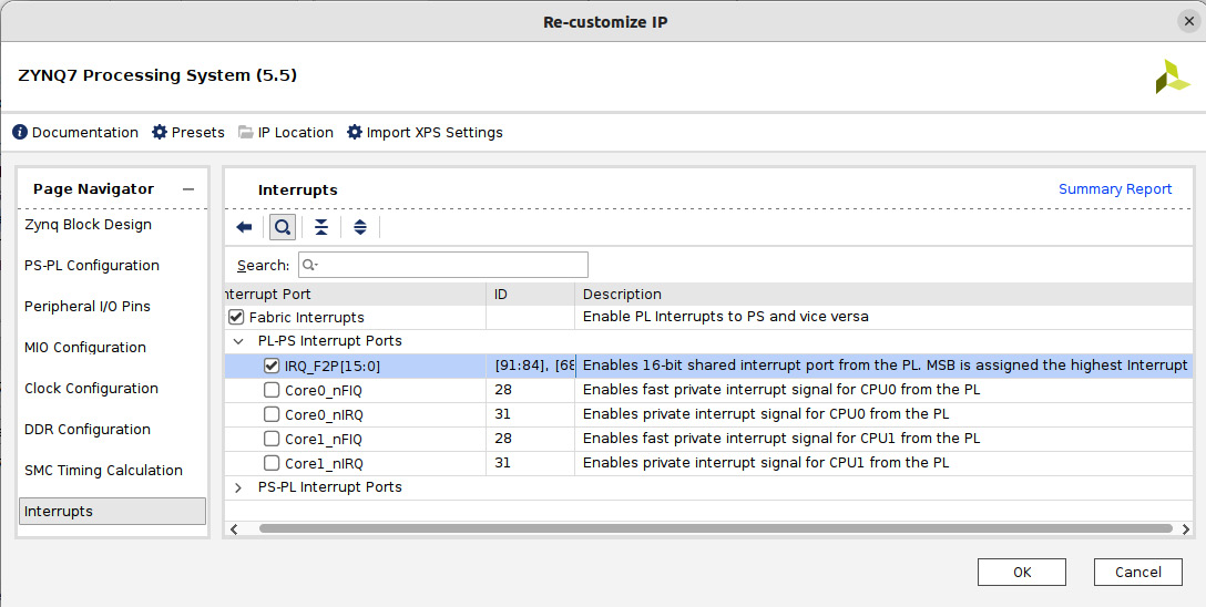
Figure 7.26 – Customizing the SoC interrupts
- Once done, click on OK. Now, let’s make sure that the customization thus far is correct. To do so, go to the Vivado IDE main menu and click on Tools | Validate Design. This will come up with no error.
The preceding steps conclude the PS customization of the generated design template. The next subsection will focus on the PL block and the required ETS SoC microarchitecture IPs, configuration, and connectivity.
Information
Further practical information on using Vivado IP Integrator to design a SoC using the Zynq-7000 PS block is available in Chapter 3 of Vivado Design Suite User Guide: Embedded Processor Hardware Design at https://docs.xilinx.com/v/u/2021.2-English/ug898-vivado-embedded-design.
Adding and configuring the required IPs in the PL block for the ETS SoC
As already mentioned, we need to design a hardware accelerator for the ETM UDP packet filtering, which will use a MicroBlaze-based Packet Processor (PP) subsystem. The PP will have an associated AXI Interrupt Controller (AXI INTC) to connect any interrupting IPs and implement the necessary IPC interrupt from the Cortex-A9 processor. The AXI INTC supports SW-generated interrupts where the Cortex-A9 writes to an AXI INTC internal register to interrupt the MicroBlaze processor. We will also add an AXI Timer and another AXI INTC to implement the IPC interrupt in the opposite direction – that is, from the MicroBlaze processor toward the Cortex-A9 processor. We will use IP Integrator to design this part of the ETS SoC.
Information
If you have closed the Vivado GUI and are reopening the tools to continue the design process, then once you launch Vivado, the list of available projects is displayed on the right-hand side of the launch screen. To open one, simply click on the project name.
Once the ETS SoC project, ets_prj_exp1, is reopened in Vivado, to restore the IP Integrator view, just click on Open Block Diagram under the IP Integrator row in the Flow Navigator pane of Vivado, located on the left-hand side menu in the GUI. Now, we will add the MicroBlaze processor subsystem to implement the PP design:
- Click on the + sign at the top of the IP Integrator window. The IP selection filter will open. Type microblaze into the filter field, and then you will see the relevant IPs displayed, as shown in the following figure. Select MicroBlaze from the list and hit Enter.
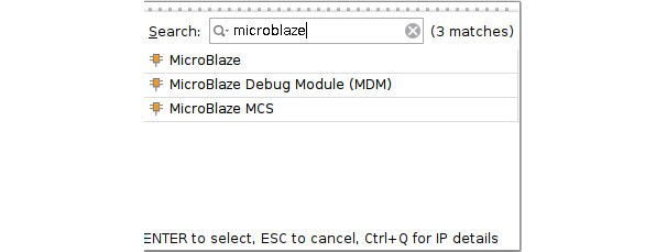
Figure 7.27 – Searching for the MicroBlaze IP in the IP Integrator
- Once the MicroBlaze IP has been added, click on the Run Block Automation hyperlink that appears in the IP Integrator main window, as shown here.
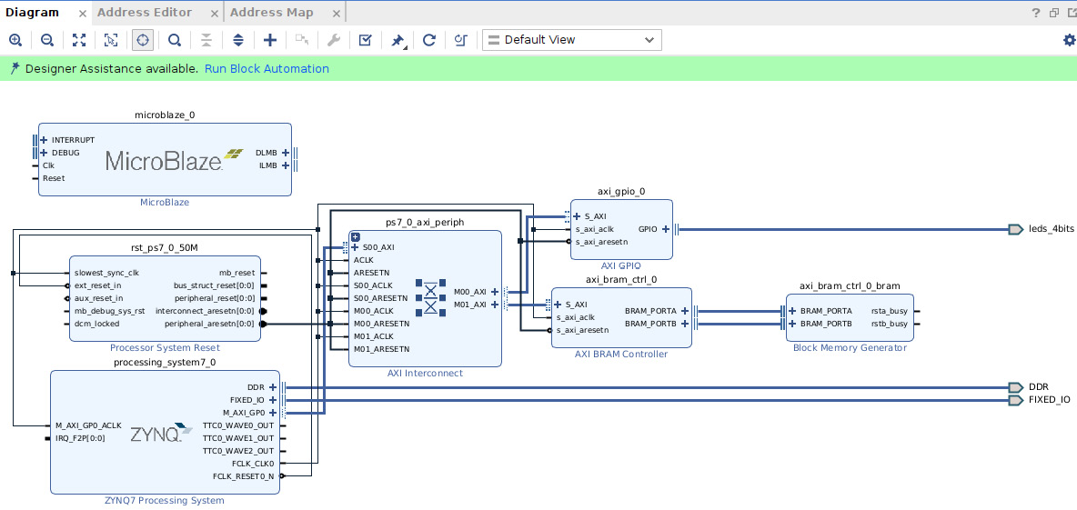
Figure 7.28 – Launching Run Block Automation in the IP Integrator
- This will open the MicroBlaze subsystem configuration wizard. Set its configuration as shown here and click OK.
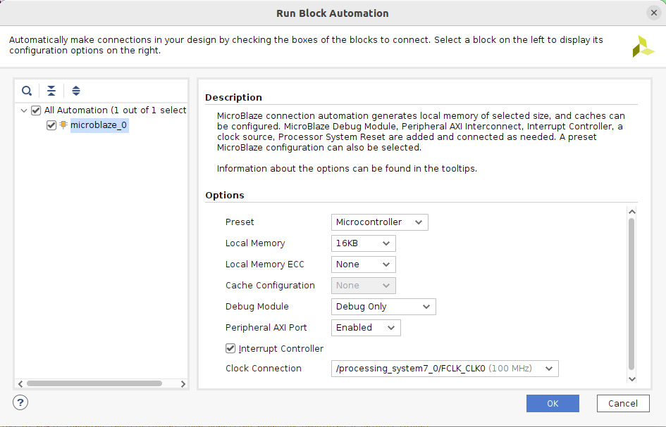
Figure 7.29 – Configuring the MicroBlaze subsystem in the IP Integrator
- Once the MicroBlaze processor is configured, remove the MB AXI interconnect from the PL subsystem by right-clicking on it and then selecting Delete. We will use a single AXI interconnect in the PL block to network both the MicroBlaze subsystem and the PS.
- We need to customize the MicroBlaze-embedded processor subsystem. In the IP Integrator main window, double-click on the MicroBlaze instance added to the design. This will open the MicroBlaze customization window, as shown in the following screenshot. Select Microcontroller Preset in the Select Configuration field. Make sure that the other selected settings match the figure. Then, click on Next >.
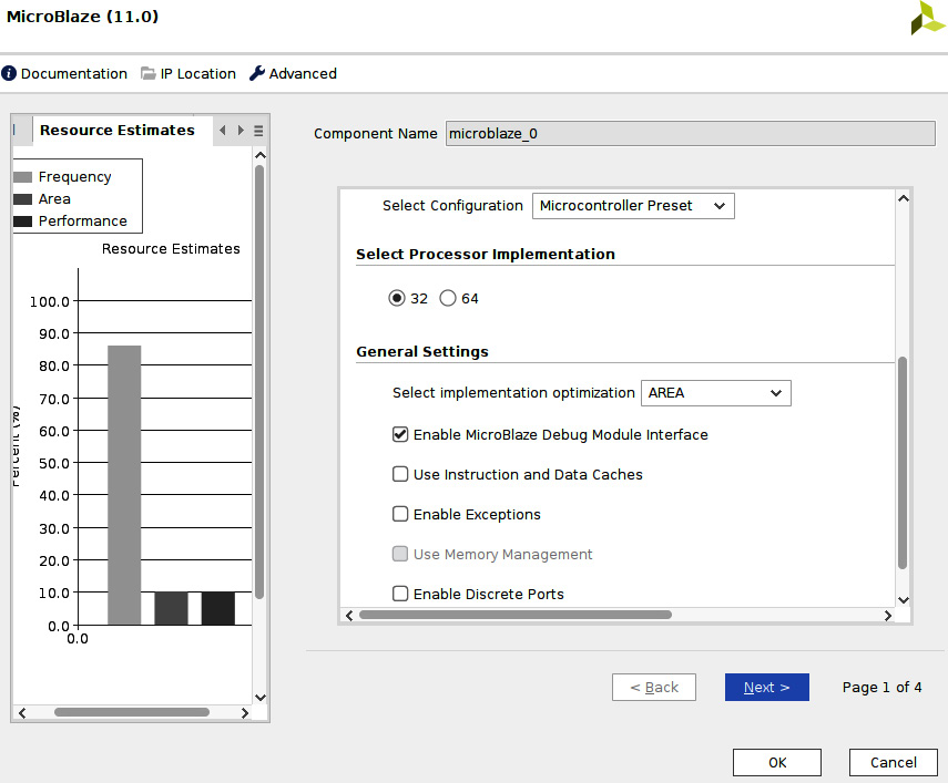
Figure 7.30 – Customizing the MicroBlaze processor for the ETS SoC (window one)
- This will open the next MicroBlaze processor configuration window. In the Optimization section, select PERFORMANCE and set all the other parameters, as shown in the following figure. Then, click Next >.
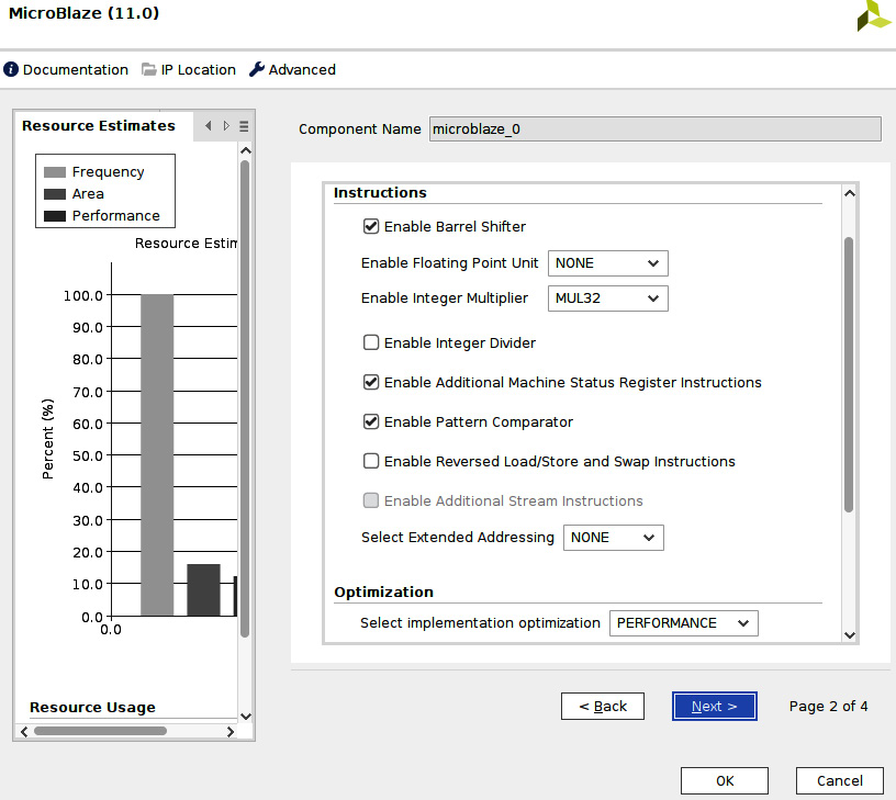
Figure 7.31 – Customizing the MicroBlaze processor for the ETS SoC (window two)
- In the third MicroBlaze IP configuration window, select BASIC as the Debug mode and leave the other fields as their defaults. Then, click Next >.
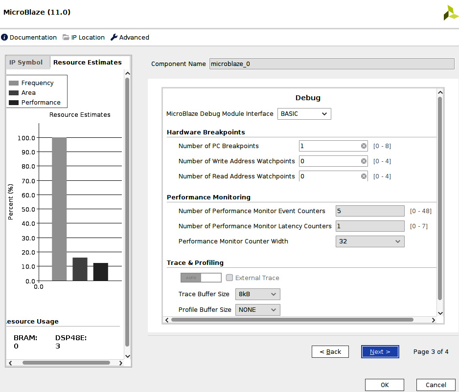
Figure 7.32 – Customizing the MicroBlaze processor for the ETS SoC (window three)
- Once the fourth MicroBlaze IP configuration window is open, make sure that the Local Memory Bus (LMB) is enabled for both the instruction and data sides of the processor. We intend to run the MicroBlaze-embedded software from the LMB memory, which provides local SRAM with fast access. Make sure that all the other settings match the following figure. Then, click on OK.
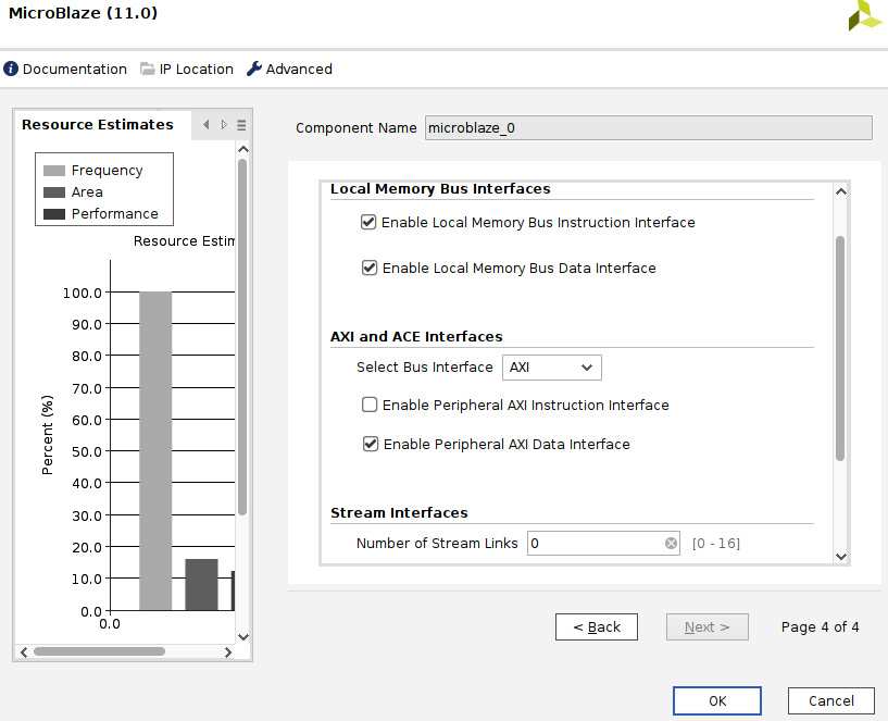
Figure 7.33 – Customizing the MicroBlaze processor for the ETS SoC (window four)
- Now, double-click on the PS AXI interconnect (ps7_0_axi_periph) and configure it for the desired number of slave and master ports, as shown in the following figure. Then, click OK.
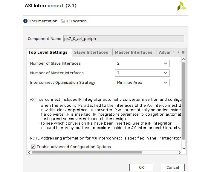
Figure 7.34 – Configuring the PL AXI interconnect slave and master ports
Information
Make sure that the Interconnect Optimization Strategy option in the preceding AXI Interconnect configuration window is set to Minimize Area. This will prevent hitting a known issue with Vivado IP Integrator, which should come up with an error code, [BD 41-237] Bus interface property ID_WIDTH does not match, if Interconnect Optimization Strategy is not set to Minimize Area.
- Connect the MB AXI Data Master (M_AXI_DP) port to ps7_0_axi_periph, and do the same for all the MicroBlaze peripherals. The resulting system should look like the following figure.
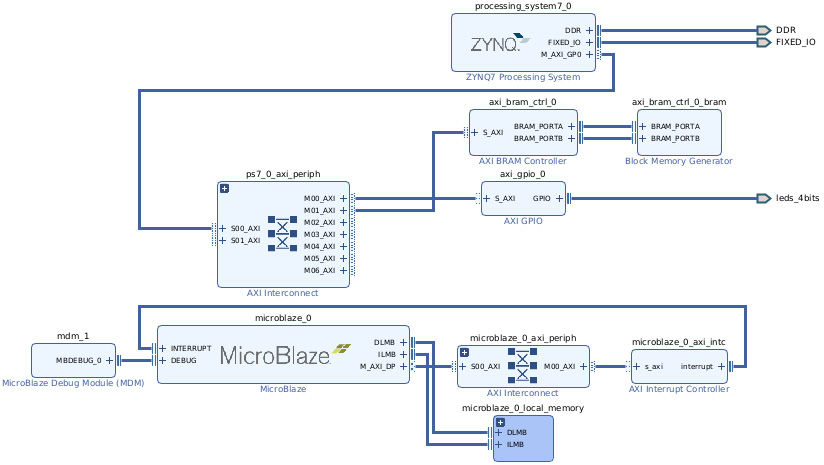
Figure 7.35 – The PL subsystem view following the customization
- Now, we will add the AXI Timer, and then click on the Run Connection Automation command suggested by Designer Assistance in IP Integrator. We will then complete the process manually and connect the AXI Timer interrupt output to the MicroBlaze AXI INTC (microblaze_0_axi_intc) via the concatenation vector (xl_concat_0). The second entry of the concatenation vector is from the MicroBlaze Debug Modem (MDM), as highlighted in the following figure.
Figure 7.36 – MicroBlaze processor subsystem interrupts connectivity
- To implement the IPC interrupt from the MicroBlaze to the Cortex-A9, we can use a second AXI INTC instance. Add an AXI INTC using the IP Integrator. At the AXI INTC IP configuration stage, select 8 for Software Interrupts in the Advanced configuration tab. The following figure shows the desired configuration for the second AXI INTC IP.
Figure 7.37 – Adding an AXI INTC for the IPC interrupt from the MicroBlaze to the Cortex-A9
- Now, we need to connect the second AXI INTC axi_intc_0 interrupt output to the IRQ_F2P interrupt input of the PS block that we enabled previously when customizing the PS block. We simply need to right-click on the axi_intc_0 interrupt output port, which will bring up the menu as shown here. Select Make Connection….
Figure 7.38 – The IP Integrator signal connectivity feature
- The following figure will open with the possible connection options for the AXI INTC interrupt output signal. Select the desired port, IRQ_F2P, and click OK.
Figure 7.39 – Connecting the AXI INTC interrupt output to the IRQ_F2P PS input
- We should have all the IPs required to build the PP, based on a MicroBlaze processor that is included, configured, and connected using the IP Integrator GUI. The resulting subsystem should look like the following figure.
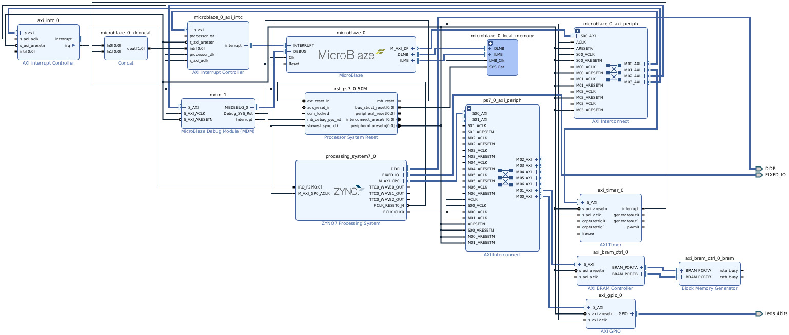
Figure 7.40 – The PS and PL subsystem view following the customization
- We should now proceed to the subsystem address mapping by selecting the Address Map tab in the IP Integrator main window, which will open the system Address Map view. This needs to be set up to match the customization desired in the PP subsystem. There are unassigned regions and excluded regions by default. To include more IPs as visible regions in the MicroBlaze address map or the PS master address map, first expand the MicroBlaze address map region, select the IP or IPs to add, right-click on the IPs, and click on Assign, as shown in the following figure.
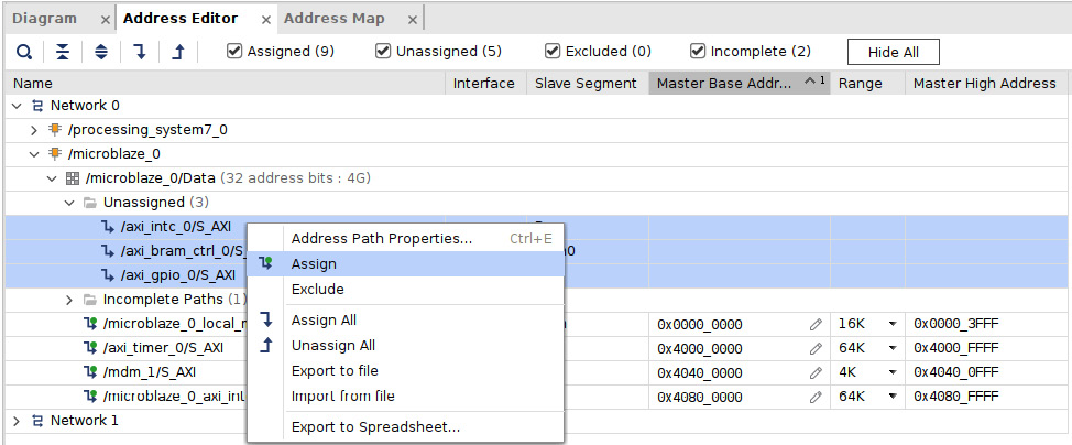
Figure 7.41 – Assigning IPs to the MicroBlaze data side address map region
- Once an IP has been assigned, it now needs to be included in the address map by right-clicking on the IP row and then clicking on Include.
- The MicroBlaze data address map should look like the following:
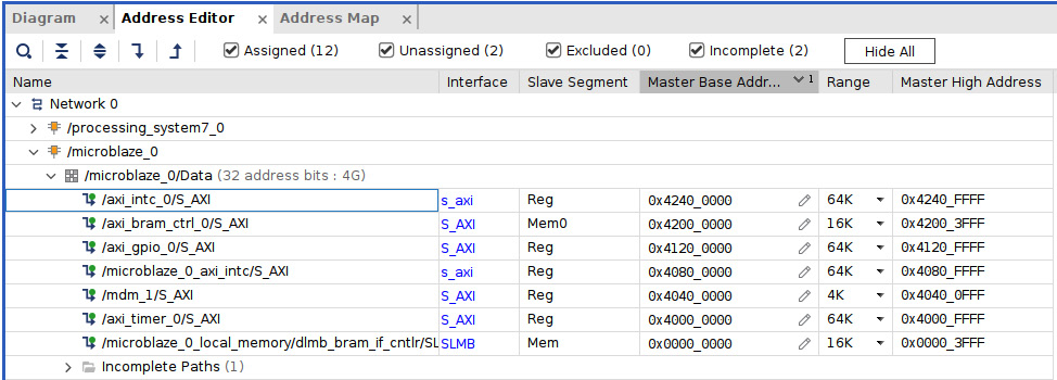
Figure 7.42 – The MicroBlaze data side address map
- The PS master visible address map within the PL block needs to be configured to look like the following figure. You can use the same techniques described for the MicroBlaze address map customization to set it up.
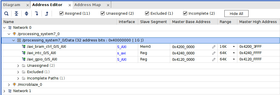
Figure 7.43 – The PS master address map
- We can increase the MicroBlaze LMB size to 16 KB in anticipation of the MicroBlaze software being more than the allocated 8 KB in the preset. Expand Network 1 in the preceding figure and then set the LMB size to 16 KB. Click on the Diagram tab of IP Integrator to return to the system view.
- Go to the Vivado IDE main menu and click on Tools | Validate Design. This should return no errors on the ETS SoC design.
Information
Further practical information on using Vivado IP Integrator to design a MicroBlaze-based embedded processor subsystem is available in Chapter 4 of Vivado Design Suite User Guide: Embedded Processor Hardware Design at https://docs.xilinx.com/v/u/2021.2-English/ug898-vivado-embedded-design.
Understanding the design constraints and PPA
This section will briefly cover Power, Performance, and Area (PPA) analysis and the physical design constraints required when the SoC RTL is implemented by the tools targeting the FPGA technology.
What is the PPA?
PPA is an analysis we usually perform on a given target IP when designing an SoC for the ASIC technology. This is performed to evaluate its characteristics under these metrics. This analysis provides us with an idea of the IP requirements before the IP is physically implemented in the actual ASIC device. The study helps us in understanding the following:
- The IP consumption in terms of power, measured in watts. The static power is consumed by simply powering up the IP and the dynamic power when the IP executes the type of workload it is supposed to perform.
- The maximum clock frequency measured in MHz at which the IP can run, which will give us an idea of whether the IP meets the system requirement in terms of performing the tasks at the speed needed.
- The IP size in terms of the silicon area needed to implement it within the target SoC, measured in µm² to perform the required functionality. This also includes any storage it may require, such as SRAM and Read-Only Memory (ROM).
Although for the FPGA these metrics can be measured by simply implementing the design (or a cut-down version of it to only include the IP on its own), when the design or the IP is available, we still need to know these values prior to the implementation trials. These figures help in dimensioning the FPGA capacity, its speed grade, and the supporting circuits to use on the electronics board, such as the power supplies and external storage.
Also, when selecting an FPGA for our SoC, many choices of the implementation decision are already implicitly made by the FPGA technology vendor. This means that we are in the process of choosing the optimal device that can host our SoC; usually, we should oversize by some margin for future expansion, just in case there is a need to add a feature or adjust an IP capability once deployed in the field. This is an FPGA, which means that it can be reprogrammed or patched at any moment, and that can be after the solution deployment.
We will briefly cover this subject in this chapter to provide an overview of what PPA means for FPGA designs. You are encouraged to research the topic further to make physical design decisions that may affect the overall success of your project. When implementing an SoC following all the design stages covered thus far in Part 2 of this book, we need to understand that a given IP needs resources to be implemented and mapped to the FPGA available logic.
Information
You are encouraged to study the PPA topic further if you are not familiar with these metrics; ARM provides a good tutorial on the subject that can be accessed at https://developer.arm.com/documentation/102738/0100/?lang=en.
Synthesis tool parameters affecting the PPA
The way an IP is synthesized and implemented by tools may affect the target IP PPA. If the logic elements to which the RTL has been mapped are geographically located closer to each other and use the fastest available nets for interconnections, the result may be a fast IP able to run at high frequencies. Sometimes, we need to make compromises between design speed and the required space within the FPGA. Also, the larger a design is in terms of silicon area, the more static and dynamic power it requires to deliver the performance we are after. Many other interdependencies need to be understood before setting up the required constraints at all the design stages, in order to guide the implementation tools to achieve our design implementation objectives. The synthesis tools have many techniques at hand to try and achieve a design objective, such as the following:
- Register replication to augment the fan-out or reduce the net delays of the connecting signals of two logic elements that are geographically far apart in the silicon area.
- Finite State Machine (FSM) encoding, which affects the area and the speed at which FSM can run.
- Merging and optimizing logic by eliminating duplicate logic, such as registers used for synchronization during the input or output of an IP, which when connected may end up using both. However, sometimes we want this to be the case.
There are many options and attributes that we can specify for the synthesis tool to guide its optimization strategy and, therefore, affect the PPA outcome. Usually, there are profiles for speed, area, or a balanced strategy that presets all the synthesis parameters to a default value without the requirement to set each one of them. It is good to familiarize yourself with these to understand how these parameters affect the outcome of the synthesis stage and, if needed, to tune them to produce a different or better outcome. Chapter 2 of Vivado Design Suite User Guide: Synthesis provides a detailed list of all the available attributes that a user can set at this first stage of the FPGA design implementation, which can be found at https://www.xilinx.com/content/dam/xilinx/support/documents/sw_manuals/xilinx2022_1/ug901-vivado-synthesis.pdf.
Specifying the synthesis options for the ETS SoC design
We first need to generate the design RTL files for the ETS SoC project using the Vivado GUI, as indicated in step 1; then, we can proceed to specify the project synthesis constraints following step 2 and step 3:
- On the Flow Navigator page, click on Generate Block Design. The following window will open. Use the default values, except for the number of jobs. These will make use of parallel processing using several processors, up to the ones dedicated to the Linux UbuntuVM, or the number of physical CPUs on your machine if you are using a native OS. Click Generate.
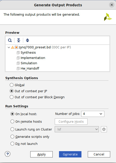
Figure 7.44 – Generating the ETS SoC project RTL file
- To set the ETS SoC project synthesis options, including the synthesis constraints, in the Vivado GUI main menu, go to Flow, then Settings, and then select Synthesis Settings…, as indicated by the following figure.

Figure 7.45 – Opening the synthesis entry window
- The following Synthesis menu will open, where you can examine the different constraints available. When a constraint is selected, a description is provided at the bottom, as indicated in the following figure. Leave the options at their default values and click OK.
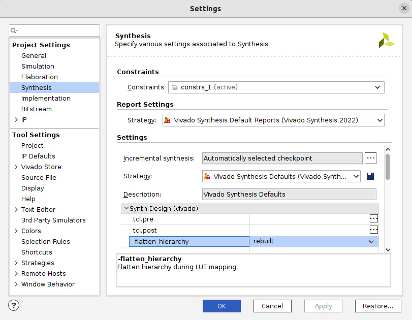
Figure 7.46 – Setting the synthesis constraints for the ETS SoC project
Implementation tool parameters affecting the PPA
Once the SoC design has been synthesized and the RTL has been converted into an FPGA-specific netlist, guided by the synthesis tools option to meet our PPA strategy, the next step is to implement the logical netlist to the physical elements of the FPGA resources. This physical implementation and mapping is a complex software-driven process with many optimization strategies, which are also guided by the user via design constraints. There are three types of FPGA implementation constraints:
- Physical constraints, defining the mapping between the logical elements in the netlist and their physical equivalent in the FPGA resources. These include the I/O pins, the physical placement of block RAMs, and the device configuration settings.
- Timing constraints, defining the clock frequency for the design. These are specified in a format defined by Xilinx called Xilinx Design Constraints (XDCs).
- Power constraints, defining the parameters for the power analysis. They include the operating conditions (voltage, power, and current settings) and the operating environment. They also specify the switching activity rates for the design’s physical objects (nets, pins, block RAMs, transceivers, and DSP blocks).
These design constraints help to drive the Vivado implementation tools at every stage of the process and guide them toward an optimization strategy, in terms of logic, power, and physical placements.
The physical design within modern FPGA devices is becoming an engineering discipline worth the specialism, considering what it requires in terms of techniques and the learning curve. You are encouraged to explore this domain further using Vivado Design Suite User Guide: Implementation for Xilinx, available at https://docs.xilinx.com/viewer/book-attachment/FwU2AZhBjPWyTDgTpfvMrg/3OSTgfIjc~pSJ2lU_YabuQ.
Specifying the implementation options for the ETS SoC design
The steps for this are as follows:
- To enter the implementation options, like for the synthesis settings specification, go to Flow, then Settings, and then select Implementation Settings.
- The following Implementation menu will open, where you can examine the different available settings. When a row is selected, a description is provided at the bottom, as indicated in the following figure. Leave the options at their default values and click OK.
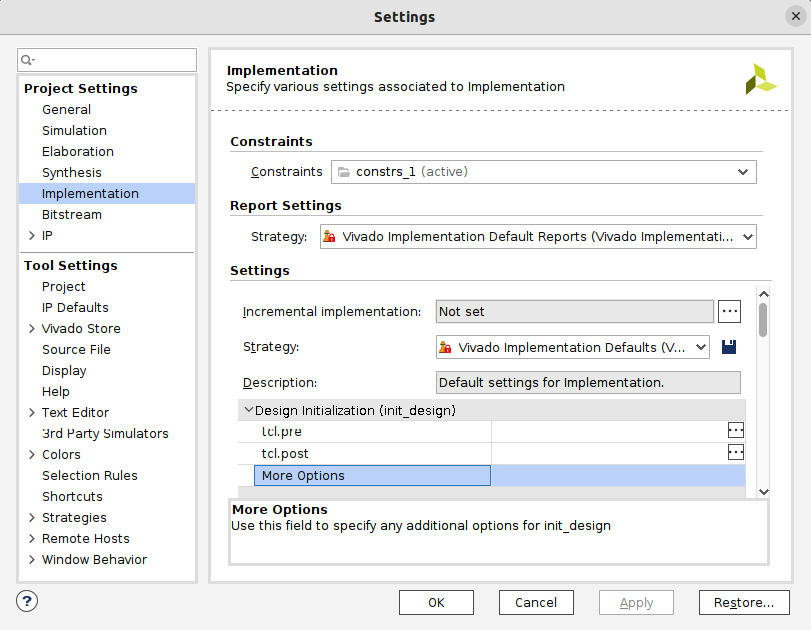
Figure 7.47 – Setting the implementation settings for the ETS SoC project
Specifying the implementation constraints for the ETS SoC design
The steps for this are as follows:
- To enter the implementation constraints, in the Vivado GUI Flow Navigator, go to Implementation | Open Implemented Design | Constraints Wizard. We already have the timing constraints defined for the preset template, which we kept for the ETS SoC design and can be examined in Step 2.
- To enter or view the timing constraints, in the Vivado GUI Flow Navigator, go to Implementation | Open Implemented Design | Edit Timing Constraints. This will open the following window, where the timing constraints can be edited.

Figure 7.48 – Editing the timing constraints for the ETS SoC project
Information
You can specify the timing and other design constraints for both the synthesis and implementation and add them as an XDC file to the design project. For more information, please check out Vivado Design Suite User Guide: Using Constraints, available at https://docs.xilinx.com/viewer/book-attachment/4dVZhvUrG0H01LbNfj76YA/VjEOZSdbHCzk6bRsAvMLfg.
SoC hardware subsystem integration into the FPGA top-level design
Since we have started the ETS SoC design from a template project that already had a top-level HDL wrapper generated (zynq7000_preset_wrapper.v), the project is already set for a full implementation flow, and there is no need to instantiate it within a higher-level design. Conversely, if the project was started from scratch and we used IP Integrator to generate the design, as we did in Chapter 2, FPGA Devices and SoC Design Tools, we could simply right-click on the IP-generated project and select Create HDL Wrapper to generate the top-level RTL, or use it as an instantiation template at a higher level of hierarchy. The following figure illustrates how to create the HDL wrapper for the IP design.
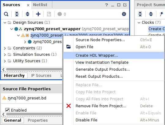
Figure 7.49 – Generating an HDL wrapper for instantiation in a higher level of hierarchy project
Verifying the FPGA SoC design using RTL simulation
The ETS SoC design project was started from a template design created by Xilinx Vivado for a known board, and then it was customized to add the PP into the PL block. The preset design already had a test bench included to test the AXI GPIO and AXI BRAM that initially formed the PL block. We can keep the same test bench for our simulation purposes, but since we have customized the address map of the ETS SoC design, we need to adjust the addresses used in the test bench to their new values. We can also extend it to verify other PP IPs to ensure their correct hardware functionality and integration. The test bench uses an AXI Verification IP (VIP), which is provided by Xilinx in the Vivado verification library to test the proper functioning of connectivity between AXI masters and slaves in the custom RTL design flow, such as in the ETS SoC project. We can add a test for the AXI INTC IP, which adds the IPC interrupts from the MicroBlaze to the Cortex-A9 processor.
Information
More information on the Xilinx AXI VIP is available at https://www.xilinx.com/products/intellectual-property/axi-vip.html.
Customizing the ETS SoC design verification test bench
Let’s customize the test bench provided in the ETS SoC initial design template by following the following steps:
- In the ETS SoC project within the Vivado GUI, locate the test bench source code, as illustrated here, and then double-click it to open it in the Vivado Source Code Editor.
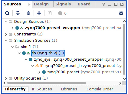
Figure 7.50 – Opening the ETS SoC project simulation test bench
- The AXI GPIO IP in the ETS SoC project address map is still at 0x4120_0000; however, we have moved the AXI BRAM from 0x4000_0000 to 0x4200_0000. In (zynq_tb.v), edit the lines accessing the AXI BRAM and change the address used for both the write and read statements from 32’h40000000 to 32'h42000000.
- We can also test the IPC interrupt mechanism between the MicroBlaze and the Cortex-A9 processor using the AXI INTC SW-generated interrupt mechanism. To generate an SW interrupt using the AXI INTC, we first need to enable (unmask) the SW interrupt using the IER register. The IER register is at the AXI INTC, [[base address] + 08h]. The IER register has eight bits we selected for the SW-generated interrupts at its customization stage. It has no hardware pins or interrupt-connected inputs. Now, to generate an SW interrupt using the AXI INTC, we simply need to write to the corresponding bit of the ISR register, which is one of the ISR[7:0] bits. The ISR register is at offset 0x00 from the AXI INTC base address. The base address of the AXI INTC is at 0x4240_0000. In the test bench (zynq_tb.v), add the following lines after the end of the AXI GPIO test and just before the start of the AXI BRAM test:
// Testing the AXI INTC Interrupt Controller
$display ("Writing to the AXI INTC IER[0] to Enable the SW IRQ");tb.zynq_sys.zynq7000_preset_i.processing_system7_0.inst.write_data( 32'h42400008,4, 32'h1, resp);
repeat(10) @(posedge tb_ACLK);
$display ("Writing to the AXI INTC to generate SW IRQ");tb.zynq_sys.zynq7000_preset_i.processing_system7_0.inst.write_data( 32'h42400000,4, 32'h1, resp);
repeat(10) @(posedge tb_ACLK);
$display ("Reading from the AXI INTC to check that the SW triggered Interrupt is pending"); tb.zynq_sys.zynq7000_preset_i.processing_system7_0.inst.read_data(32'h42400004,4,read_data,resp);repeat(10) @(posedge tb_ACLK);
if(read_data == 32'h1) begin
$display ("AXI VIP SW Interrupt Generation Test PASSED");end
else begin
$display ("AXI VIP SW Interrupt Generation Test FAILED");end
- Let’s go back to the IP Integrator window and make sure that the PS-PL configuration matches the following figure to avoid an unresolved issue in the AXI VIP.
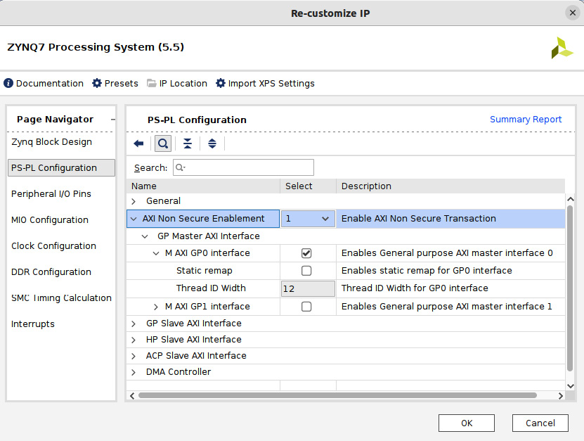
Figure 7.51 – The PS-PL GP slave AXI interface settings to use for the ETS SoC design
Information
There is a known simulation issue with the AXI VIP that we can hit if we don’t set the PS-PL GP slave AXI interface as shown in the previous figure. For further details on this issue, please check out https://support.xilinx.com/s/question/0D52E00006hplh2SAA/axi-simulation-bug?language=en_US.
Hardware verification of the ETS SoC design using the test bench
We have thus far explored the test bench provided by the Vivado design template, then customized it to match our settings, and finally, expanded it to use the AXI VIP to test the IPC interrupt mechanism. We have chosen a microarchitecture implementation that uses a doorbell register to generate the IPC interrupt, from the MicroBlaze in the PP within the PL block to the Cortex-A9 within the PS block. We can now load the test bench and run the simulation in Vivado:
- In the Vivado Flow Navigator, select Simulation | Run Simulation | Run Behavioral Simulation.
- The test bench will be loaded, and the simulation will start up to the initialization stage. To run the simulation, in the Vivado GUI main menu, go to Run | Run All. This will run the simulation to completion. We have two sets of results to examine, the simulation waveform and the Tcl Console printing the output of the display statements from the test bench.
- The simulation waveform looks like the following figure. We can see the transactions from the AXI GPIO, then the AXI INTC, and then the last one from the AXI BRAM.
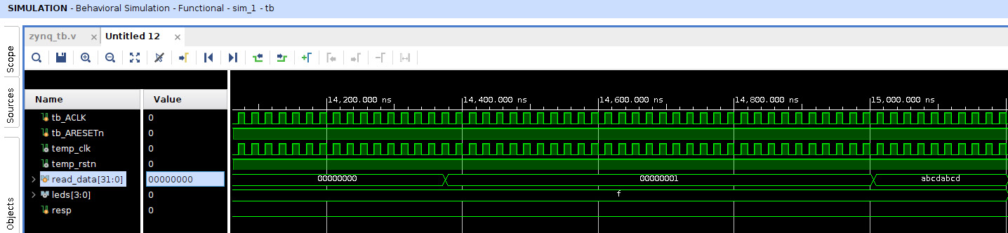
Figure 7.52 – The ETS SoC design RTL simulation waveform
- The simulation console output is more verbose and displays the transaction flow and the display statement from the test bench. The tests are passing, and the results are as expected. It looks like the following:
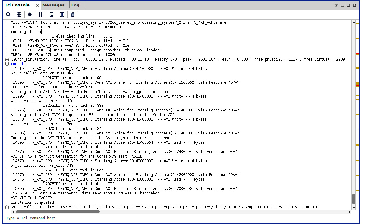
Figure 7.53 – The ETS SoC design RTL simulation Tcl Console output
Implementing the FPGA SoC design and FPGA hardware image generation
As already introduced in Chapter 2, FPGA Devices and SoC Design Tools, of this book, the design implementation takes the design netlist and the user constraints (including the implementation settings) as input and produces the physical design netlist. This physical netlist is then mapped, placed, and routed using the FPGA hardware resources and meeting (when possible) the user constraints. Once the physical netlist is produced, the FPGA image or the bitstream file is generated to configure the FPGA device. The FPGA device PL block can be programmed via JTAG when still in the debugging stages of the design, or by the PS. In the debugging stages of the SoC, the configuration is done through the Xilinx FPGA JTAG interface. The bitstream is then downloaded directly to the FPGA PL block from the host development machine using a JTAG cable, connecting the host machine to the FPGA board.
ETS SoC design implementation
We have already introduced the implementation constraints and settings in the PPA section of this chapter. The only action we need to perform now to implement the design, once its RTL files have been synthesized and its netlist has been produced, is to launch the implementation step from the Vivado Flow Navigator by selecting Implementation | Run Implementation. This will take some time to accomplish, according to how much system memory and how many CPUs are used to perform the task, as the jobs associated with the implementation can be parallelized. If the design can meet the specified constraints, then the implementation will finish with no errors, and we can then proceed to generate the FPGA bitstream.
ETS SoC design FPGA bitstream generation
To open the FPGA bitstream file generation options menu, in the Vivado GUI, go to PROJECT MANAGER in the Flow Navigator section, and then select Settings. Once the Settings menu is open, select the Bitstream row, which will open the following window.
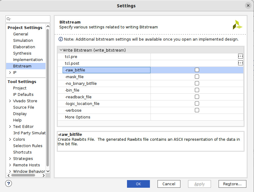
Figure 7.54 – The FPGA bitstream file generation options
In the preceding menu, most of the options are related to the FPGA configuration operational control, such as during a cyclic readback of the FPGA bitstream once deployed in the field. The read-back file from the FPGA is then compared to a known good bitstream file stored on non-volatile memory to make sure that it didn’t get corrupted due to environmental issues, such as Single-Event Upsets (SEUs).
Once both the hardware and the software designs are debugged and have reached a certain level of development maturity, the FPGA bitstream can be stored in non-volatile memory on the electronics board, from which the FPGA is automatically configured on the system power-up by the PS. We will cover the configuration and boot modes later in this book.
Information
The following article provides details on the supported non-volatile storage for booting and configuring the Zynq-7000 SoC FPGAs: https://support.xilinx.com/s/article/50991?language=en_US
Summary
In this chapter, we started by providing some operational and practical guidance on how to install and use the Xilinx SoC development tools on an Ubuntu Linux VM, built and hosted on Oracle VirtualBox. We revisited the ETS SoC architecture requirements and defined a microarchitecture based on a PP engine that uses a MicroBlaze processor subsystem to implement the Ethernet frames filtering hardware acceleration. We used a Vivado example project preset for a known Xilinx Zynq-7000 SoC board as a starting template design, and we also customized the PS block to match the microarchitecture requirements. We extended the template design by building all the required functionalities in the PL block, using IPs from the Vivado library. We went through a full customization process to design the hardware of an embedded system in the PL block based on the MicroBlaze. Additionally, we put in place the necessary infrastructure for the IPC between the Cortex-A9 and MicroBlaze as needed by the envisaged ETS SoC software architecture, which we will implement in Chapter 8, FPGA SoC Software Design Flow. We also covered hardware verification using an RTL test bench to simulate the ETS SoC design, and we checked that the introduced customization didn’t break the initial template design functionality and that the added IPC features were working as expected. We also introduced the PPA concept and its important aspects for a successful SoC project. We looked at the FPGA design constraints for both the synthesis and the implementation stages, how to specify the settings for these flows, and how to enter the design constraints that influence the achieved implementation results. Finally, we covered the design implementation flow, from synthesis to the FPGA bitstream generation.
The next chapter will continue by using the same practical approach for the software implementation flow for the ETS SoC design.
Questions
Answer the following questions to test your knowledge of this chapter:
- How is communication established between the main ETS SoC software and the hardware accelerator? Are there any alternative approaches you can think of?
- How can we augment the capabilities of the proposed microarchitecture and scale it for future needs?
- Why is the TS field used in the ETMP UDP packet?
- Which field in the ETMP UDP packet is processed better in hardware instead of the MicroBlaze software? Why?
- What are the advantages of starting the ETS SoC design from a template preset?
- Describe the steps needed to augment the number of IPC interrupts between the Cortex-A9 and the MicroBlaze processors from 8 to 16 interrupts.
- What is the frequency we chose to run the PL logic at? How can we increase it to 125 MHz?
- How can we check that the aforementioned increase of the PL logic frequency to 125 MHz is okay for the ETS SoC project?
- How are the PL interrupts targeting the Cortex-A9 connected?
- How can we test that the design customization performed in IP Integrator is in line with the Vivado tools' expectations for the ETS SoC project?
- In the address map view of IP Integrator, why do we have two networks?
- In the address map, under Network_0, why do we have two address maps?
- How can PPA influence the success (or lack of suuccess) of the ETS SoC project?
- What are the design constraints? Why do we use them? How can we specify them in Vivado for the ETS SoC project?
- What were the changes needed to customize the preset RTL test bench for the ETS SoC project?
- How can we check that the design is meeting the expected functionality using simulation?
- What is an FPGA bitstream? And how can it be loaded to the FPGA device?
- How could an FPGA-based SoC design get corrupted due to its bitstream while deployed in the field? How could we monitor and correct such behavior?