
2
FPGA Devices and SoC Design Tools
This chapter will begin by providing an overview of the Xilinx FPGA hardware design flow in general and the tools associated with it, before highlighting the specific tools that are used when designing an SoC for FPGAs. We will also introduce the SoC design hardware verification using the available simulation tools. Finally, we will cover the high-level software design flow and its different steps and introduce the tools involved in the software design for an FPGA-based SoC.
In this chapter, we’re going to cover the following main topics:
- FPGA hardware design flow and tools overview
- FPGA SoC hardware design tools
- FPGA and SoC hardware verification flow and associated tools
- FPGA SoC software design flow and associated tools
Technical requirements
The GitHub repo for this title can be found here: https://github.com/PacktPublishing/Architecting-and-Building-High-Speed-SoCs.
Code in Action videos for this chapter: http://bit.ly/3fRWh8z.
FPGA hardware design flow and tools overview
This section introduces the steps involved in the FPGA hardware design and provides an overview of the associated tools, along with each step.
FPGA hardware design flow
The FPGA hardware design process is similar to the ASIC hardware design process that we covered in the previous chapter. Besides the high ASIC NRE cost and its long time to market path compared to an FPGA design process, the main technical difference is that the choice of features the designer can use and combine to produce a working FPGA device is limited by what the FPGA device itself can offer. However, there is a rich list of devices and features that usually meet many demanding and challenging system requirements. Once the FPGA design specification has been finalized and the target FPGA device has been chosen, the design flow will look as follows:
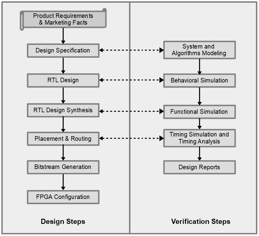
Figure 2.1 – FPGA hardware design flow
Product requirements phase
This is not a design step but rather a fundamental starting phase from which the idea of using an FPGA may have originated. Marketing facts and time-to-market guidelines are studied and a decision on the overall design budget and strategy is put in place to help the engineering teams start working on their parts.
Design specification
This step is also called the design capture step, as covered by the SoC in ASICs design flow section of the previous chapter. It is the first phase of designing an FPGA and consists of capturing the specification, HW/SW partitioning, IP selection, and defining the external interfaces. The SW portion is usually implemented externally to the FPGA in another ASIC-based SoC or a discrete CPU system. The interfacing mechanisms and the external SW to the FPGA hardware communication stack are defined in detail in this step. Alternatively, if the SW has been implemented within the FPGA, then we are in the FPGA SoC design flow paradigm, which we will cover in the next section. There isn’t much of a difference at the architecture level besides the interface’s implementation and the fact that the SW is mapped to an ARM CPU or CPUs within the processing subsystem (PS) portion of the FPGA device. Like the ASIC design flow, the design capture process could be in text format as an architecture specification document. It is also usually associated with a design capture of the specification in a computer language such as C, C++, Python, SystemC, TLM, SystemVerilog, or a combination. Many environments exist where the specification can be expressed in these languages, as follows:
- Imperas OVP, which uses the C language to build and connect system intellectual property (IP) models. For more information on this environment, please check out https://www.imperas.com/dev-virtual-platform-development-and-simulation.
- Synopsys Platform Architect, which uses SystemC and TLM to build and interconnect IP models. For more information on this approach, please check out https://www.synopsys.com/verification/virtual-prototyping/platform-architect.html.
- gem5, which uses C++ to build the system IP models and Python to specify a system model and connect the IP models. For more information on this environment, please check out https://www.gem5.org/documentation/learning_gem5/introduction/.
The design capture isn’t usually a full SoC system model – it could be just an overall description of the main algorithms and inter-block data and command passing mechanisms, which is mainly done in SystemVerilog, to prepare the overall FPGA design verification step.
For the FPGA hardware-centric applications such as those concerned with video and image processing that’s performed in the FPGA logic, complex algorithm modeling is performed using third-party tools. The translation tools that produce the RTL are often exploited as-is with the RTL module or a version of it that’s been manually tuned for the FPGA technology target device. This technique is also used in software-centric designs seeking to hardware-accelerate software (using the FPGA logic) when discovering bottlenecks while purely executing on a CPU. The latter part of this book will cover both techniques as part of designing advanced systems in FPGA SoCs.
RTL design
Like the ASIC design flow, the design capture phase is followed by the RTL design phase in Verilog, SystemVerilog, or VHDL of the FPGA modules. Their top-level files instantiate and interconnect all the modules. It is worth noting that this step is becoming a team effort due to the increased complexity of what can be implemented in a modern FPGA. Many tools’ facilities are available to make it a smooth cooperative effort.
As mentioned previously, some of the RTL is automatically produced by other software tools from a higher-level language, ready to be synthesized as an IP or part of it. High-level synthesis from C, C++, or SystemC is also supported by the tools so that you can directly contribute to generating the IP netlist.
The system design in RTL is a team effort where it is partitioned into multiple blocks. Each block will have an individual owner who coordinates their work with the other members of the team using a design code repository such as Git or Subversion, for example.
RTL behavioral simulation
The RTL design phase is then simulated using test benches written specifically to verify the functional correctness and intended functionality of the RTL design. This simulation usually involves an assertion-based verification methodology. Many RTL simulation tools support the Xilinx FPGA devices, alongside the integrated version of the simulation tools within the Xilinx software design environment. We will cover these tools in detail in a subsequent section of this chapter.
RTL design synthesis
The synthesis tool takes the FPGA RTL design files and generates a netlist, which is a machine file that translates the RTL onto specific elements of the FPGA features that have been mapped using the synthesis software library. The synthesis tool performs a complex translation job by inferring elements from the FPGA features as it recognizes a certain specific characteristic that matches them. In certain situations, it just replaces the RTL with a netlist notation when the RTL style that’s used is a direct instantiation of the desired library elements. This technique is sometimes used as an optimization technique for area or speed, where the synthesis algorithm fails to recognize the elements from a high-level behavioral description in the RTL. Hard block macros are also an example of this replacement mechanism at the synthesis stage.
Netlist functional simulation
The functional simulation is usually performed after the design synthesis phase, where the RTL design has been translated into a netlist for grouping the FPGA features. At this stage, it is no longer the RTL behavioral design we are simulating but rather the netlist translation, which has assembled many elements of the FPGA features for implementing the RTL design. It is necessary to perform this step to make sure that the translated outcome matches the intended RTL behavior and that there is no need to direct the synthesis tools to do a better job or optimize in places.
Placement and routing
In this phase, the netlist is distributed across the FPGA features, and elements are geographically placed and connected using the network of routing resources. The Place and Route (P&R) software is a complex part of the FPGA technology, and its efficiency is in finding the optimal placements to interconnect the design elements and meet the performance requirements described via the design constraints. This step is usually attained by the software after many attempts and can propose multiple results with different placement and routing. Size, speed, and power are universal metrics that drive the optimization target of the P&R tools. The tools can be requested to use a balanced approach as the design optimization objective.
Given the complexity and size of modern FPGA designs, the P&R stage can be performed on partitions of the design where limited changes have been introduced to the design once its implementation has been started. This won’t cause a long tool runtime like that of starting the implementation process afresh. This is called implementation with incremental compile, which can be specified in this situation. It can reduce place and route runtimes and preserve existing implementation optimal results.
Timing simulation
The timing simulation is usually performed after the P&R phase, where the netlist has been mapped to the FPGA resources and the connectivity between the design elements has been established in a scenario that meets the design constraints specified by the designer. At this stage, we are no longer simulating the RTL behavior or its logical representation as a netlist – it is the model of the physical implementation that is being simulated. This accounts for the elements’ timing characteristics and response, as well as the routing nets physical delays. These delays introduce all sorts of internal skews and irregularities that we try to visualize in a timing-driven simulation and check that the physical implementation still meets the design timing constraints. Any issues that the tools couldn’t resolve are spotted and corrective actions are taken – either manually by manually floor-planning regions of the design or iteratively by going back to the RTL or even to the micro-architecture and resolving the issues at the source.
Timing analysis
This analytical step is performed on the Timing Reports and guided by the Timing Simulation in areas of concern that the designer needs to study to understand the timing characteristics and budget of the design. Areas of concern are resolved, as mentioned in the Timing simulation subsection, but sometimes, it is an issue that can be resolved by upgrading the FPGA device’s speed grade when the timing budget indicates that the problems or the observations are global within the design.
Bitstream generation
This is the final stage the tool goes through. It generates the binary file that will configure the FPGA to behave as the design desires. There are a few options that we will cover later regarding the method by which the FPGA device will be programmed and its startup sequence characteristics. These are specified as options that the bitstream generation tools must account for. Security and authentication options are also specified at this stage, which we will cover in Chapter 11, Addressing the Security Aspects of an FPGA-Based SoC.
FPGA configuration
When powered up, the FPGA device needs programming to behave as specified by the design via the generated bitstream configuration file. Many methods can be used to configure the FPGA device, and each has a specific interface associated with it. For example, you could go over the JTAG interface of the FPGA when still in the debugging phase of the design and perform the initial electronics board bring-up. We will delve into these for a specific device technology such as the Zynq-7000 SoC, although most of the interfaces are common to all FPGAs except for paths over specific hardware features, such as the PS blocks in the SoC FPGAs, which are unavailable in generic non-SoC FPGA devices.
FPGA hardware design tools
The Xilinx FPGA design environment is called Vivado. It is a complete design platform that uses machine learning (ML) algorithms to reduce the FPGA implementation time. It supports all the steps in a Xilinx FPGA design flow, including creating, verifying, implementing, and validating its design. Xilinx provides two versions of the Vivado design suite:
- The ML version, which is a standard and free edition
- The Enterprise edition, which requires purchasing a license for the extra features and the added supported devices
This book will use Vivado ML version 2021.2, which can be downloaded from the Xilinx website for free and does not require a license. You are encouraged to acquire the Vivado ML from the Xilinx website, check the host machine hardware and software requirements, and follow the instructions to install it, as indicated by the Vivado Release Notes, which you can find at https://www.xilinx.com/support/documentation/sw_manuals/xilinx2021_2/ug973-vivado-release-notes-install-license.pdf.
The Vivado ML is an integrated design environment (IDE) that supports two modes of the design flow: project mode (PM) and non-project mode (NPM). In the PM, the Vivado IDE manages the design flow process and maintains its database, whereas, in the NPM, it is the user who manages the design sources and executes the design steps by providing the appropriate commands to the specific tool involved at that specific step – for example, synthesis, simulation, and implementation. Every tool has a given binary name by which it is called from the command line, along with the command options that the user can perform on the input files involved at this specific step of the design flow.
In PM, the Vivado design suite uses a project file (.xpr) and directory structure to maintain the design source files, store the results of different synthesis and implementation executions, and track the project’s status throughout the design flow. Automatically managing the design data, process, and status requires a project infrastructure.
In contrast, npm is for script-based users who do not want Vivado tools to manage their design data or track their design state. The Vivado tools simply read the various source files and compile the design through the entire flow in memory.
In the tutorials associated with this book, we will be using the Vivado ML IDE in project mode. The Vivado ML IDE includes many parts, as follows:
- Vivado IP Integrator
- Vitis High-Level Synthesis
- Vivado Logic Synthesis
- Vivado Simulator
- Vivado Implementation
- Vivado Verification and Debug ILA
- Vivado Device Programmer
- Vivado Dynamic Function eXchange (DFX)
Vivado IP Integrator
The Vivado ML Edition IP Integrator is a graphical and TCL-based development flow. It is a device and platform-aware utility that allows you to auto-connect key IP interfaces, generate subsystems, and check design rules. It allows inter-IP system connectivity at the IP interface level, such as AXI or APB, thus reducing the system connectivity time.
Vitis High-Level Synthesis
The Vitis High-Level Synthesis tool enables C++ design capture and its specification to be directly synthesized and target the Xilinx FPGAs. There is no need for the designer to translate it into an RTL language first. This will help in the prototyping stage and even when using it for production when the synthesis results have been judged as optimal.
Logic Synthesis
Vivado includes an RTL synthesis tool that translates the design RTL files into an FPGA netlist ready to be implemented. It supports design descriptions in SystemVerilog, Verilog, and VHDL. The designer also provides synthesis attributes, synthesis command tool options, and Xilinx Design Constraints (XDCs) to help optimize this step in the design flow.
Vivado Simulator
Vivado Simulator is a full-featured mixed-language simulator that supports Verilog, SystemVerilog, and VHDL RTL designs. It is an event-driven simulator that supports both behavioral and timing simulations.
Implementation
Vivado Implementation provides the placement and routing software for Xilinx devices. It takes the generated netlist from the Synthesis step and produces the FPGA configuration file. It also generates many design reports to help with analyzing the device logic and routing resources utilization, timing information, power, and other design quality-related metrics.
Verification and Debug
Vivado can help with bringing up and testing the device in various ways. This includes the necessary debug IPs to put into the design, which will then allow the user to connect them to the debug software running on the host machine at runtime. Consequently, this provides system-level runtime visibility into the hardware, which helps control it by setting up trigger events to capture its states and visualize them in the host software interface.
Dynamic Function eXchange
This feature allows you to partially reconfigure a specific portion of the design without shutting down the whole FPGA and having to reconfigure all of it. Some applications may benefit from this option and use a Time Domain Multiplexing (TDM) approach to reuse portions of the FPGA to implement multiple functions and deploy them on-demand.
FPGA SoC hardware design tools
An SoC design that targets a Xilinx FPGA such as the Zynq-7000 SoC or UltraScale+ MPSoC uses the Vivado IDE and, specifically, the IP Integrator as the SoC design capture tool. The Vivado Integrated Logic Analyzer (ILA) is used to debug the hardware interactions on the PL side with the PS side and to establish software and hardware co-debug sessions on the system at runtime. Everything else from a design flow perspective is common to a generic FPGA hardware design flow and uses the same tools to synthesize, simulate, verify, implement, and generate the FPGA bitstream file.
In this section, we’ll introduce the Vivado IP Integrator and how it can easily be used to create a sample design, including the PS block and an IP from the hardware library catalog, which will be implemented in the PL side of the FPGA. The sample design to use is shown in the following diagram:
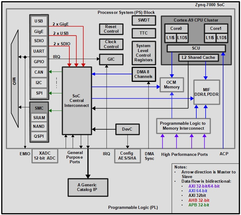
Figure 2.2 – Zynq-7000 SoC sample design
Using the Vivado IP Integrator to create a sample SoC hardware
Let’s launch the Vivado IDE and then use its IP Integrator to create the preceding sample design. The intent is to get acquainted with this step of the SoC design capture phase and become familiar with the tools rather than face a challenging design task. You will get the chance to build upon the design’s complexity as we progress throughout the different sections of this book and master the fundamental concepts. In this section, you will find steps you can follow to build the sample design. There are three phases involved in this process. First, we must create a design environment, which is simply the Vivado project using the Vivado IDE. Next, we will invoke the IP Integrator to stitch together an SoC, which is formed of the Zynq-7000 PS block and an IP from the IP catalog; the added IP will be implemented in the PL portion of the Zynq-7000. Finally, we must invoke the Vivado Generate Output Products utility to create the HDL files that corresponds to the SoC we have graphically built using the IP Integrator.
For a more detailed step-by-step description of this flow, please refer to the Vivado Design Suite Tutorial – Embedded Processor Hardware Design, available at https://www.xilinx.com/content/dam/xilinx/support/documentation/sw_manuals/xilinx2019_1/ug940-vivado-tutorial-embedded-design.pdf.
Phase 1 – creating a Vivado IDE project
Follow these steps:
- First, you must launch the Vivado IDE. Then, on the Vivado launch screen, choose Quick Start, then Create Project. Give the project a name, such as SampleProject_2, specify a location for it in your machine, and click Next. Next, specify the Project Type option as RTL Project and leave everything else as-is, as shown in the following screenshot. Then, click Next:
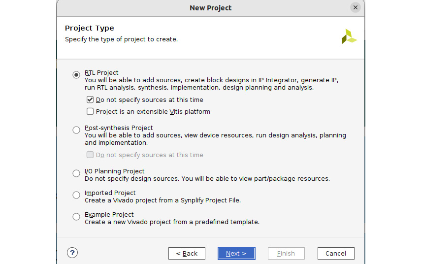
Figure 2.3 – Specifying the Vivado Project Type
- On the next page, select the Boards tab next to the Parts tab so that we can target a specific demo board rather than specify everything at the device level ourselves. The catalog of Demo Boards is rich and is also handy for learning purposes as we only need to select the Demo Board that is nearest to our learning objectives. You can order it from its vendor so that you can use it with some of the hands-on chapters in this book. We can also use it as a template and starting point for our Proof of Concept (PoC) or production design. For our exercise, we would like to target a board built around a Zynq-7000 SoC FPGA. As we can see, there are a couple. Here, we will choose ZYNQ-7 ZC706 Evaluation Board. Once selected, clicking on Next will take us to the Project Summary window. The Project Summary window gives us an idea of the details that have been captured about the target FPGA SoC device. Now, we need to click on Finish so that the project is created. At this point, the project will be created and launched.
Phase 2 – creating a processor subsystem using the Vivado IP Integrator
Follow these steps:
- On the Flow Navigator screen, go to IP Integrator and select [Create Block Design]. A dialog box will open. Name this IP subsystem design; for example, soc_design_sample_1. Leave the Directory field as its default value of <Local to Project>. Also, leave the Specify source set field as its default value of Design Sources. Click OK when you’re done. The following screenshot illustrates the desired settings:
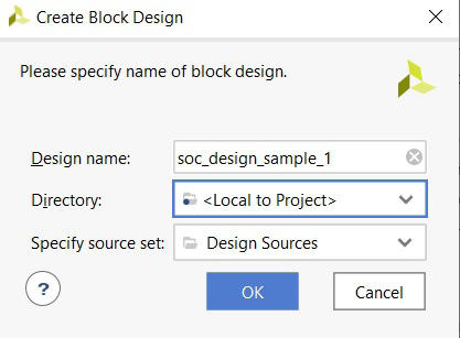
Figure 2.4 – Launching the Vivado IP Integrator
- In the Diagram window, click on the + sign to add an IP to the SoC. Then, using the dialog box that opened, type Zynq in the Search field. This will return ZYNQ7 Processing System as the only result. Select it by double-clicking on it. This will add the PS to the Diagram window. Note the Designer Assistance message that is highlighted in the green-colored row on the IP Integrator Diagram window with a command hyperlink that states Run Block Automation. Click on it. This will open the Design Wizard, which will add the FIXED_IO and DDR SDRAM interfaces to the Zynq-7000 SoC PS.
- Now, we can add more IPs manually from the PL side of the FPGA using the IP catalog. Right-click anywhere in the IP Integrator’s Diagram window and select Add IP. In the Search field, type bram to filter. You will see that there are two instances: AXI BRAM and LMB BRAM. Select AXI BRAM since we can use this IP to connect to the PS block via one of the generic AXI ports of the PS block. At this stage, the AXI BRAM needs connecting. Click on the Run Connection Automation command suggested by the Designer Assistance area of the IP Integrator. This will open the IP connection wizard. Select All Automation. You will see that the connectivity between IPs is complete. The wizard also added the Reset and AXI SmartConnect IPs.
- Now, let’s configure the size of the BRAM instance and the address mapping of the AXI BRAM controller in the SoC Address Map. Select Address Editor in the IP Integrator window. We can keep the default values as-is, which will put the AXI BRAM controller at the base address of the general-purpose GPO port facing the PL. The size of the BRAM can be changed to 32KB.
- Return to the Diagram window. Optionally, you can reshape the system diagram to get a better view by clicking on the Regenerate Layout button. Now, let’s check that the design capture is fine by running the Design Rules Check (DRC). Go to the Vivado IDE’s main menu and click on Tools | Validate Design:
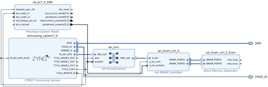
Figure 2.5 – Vivado IP Integrator – the Regenerate Layout button
Phase 3 – generating the HDL files for this design sample
Invoke the Generate Output Products utility by right-clicking on the design entry under Design Sources in the Sources window. Then, click Generate Output Products. The design HDL source files will be created.
Now, we need to create the design top-level wrapper. Right-click the top-level subsystem, soc_design_sample_1, and select Create HDL Wrapper to create a top-level HDL file that instantiates the block design of the sample SoC (PS+IP) we have just created using the IP Integrator tool. This allows us to edit the file if we wish to do so for further integrations, but for our objective, we will choose the default and click OK. The top-level wrapper HDL source file will be created and added to the top of the design.
FPGA and SoC hardware verification flow and associated tools
As shown in Figure 2.1, the design verification progresses in parallel with the steps of the design flow to make sure that the design’s functionality is preserved as the design moves forward in its life cycle. It also ensures that the required key performance indicators (KPIs) are still met. The KPIs are set at the beginning of the product and system architecture definition. They fundamentally include the system clock frequency, the design’s size in terms of FPGA device resources occupation, and the design’s energy consumption, among other parameters that the design’s performance can be measured by.
The Vivado design environment allows users to perform an RTL behavioral simulation just after the design has been captured in HDL. Once the netlist has been generated, a post-synthesis or functional simulation can be performed and, following the design implementation, a timing simulation can be run. The Vivado IDE provides an integrated simulation tool that can perform all these types of design simulations. Alternatively, the designer can choose to use a third-party HDL simulator for which Vivado IDE can generate run scripts. The Vivado IDE supports all major simulators, as follows:
- Synopsys VCS
- Siemens EDA ModelSim SE/DE/PE, and Questasim
- Cadence Xcelium
- Aldec Active-HDL and Riviera-PRO
In general, to simulate an RTL module of a design, the simulation can be driven by a test bench written in behavioral RTL and instantiating the design to simulate. The test bench is used by the simulator tool to interact with the RTL design by setting its inputs accordingly, thus capturing its outputs at an event-driven execution level. The RTL design is the design under test (DUT) and the test bench provides input to the actions the simulator will perform during the simulation execution, including the times at which certain tasks are performed. These include, but are not limited to, driving the module’s clock input, setting a given signal or input to a specific value at a specific moment in the simulation time for a finite amount of time, and capturing the results of the stimulus on the design.
The Vivado Simulator can also drive the RTL design by forcing its input, capturing its output, and displaying the results as waveforms. There are many options and utilities to choose from in this step of the design verification process. They are mostly suited for pure HDL-based systems than an SoC with a processor and software code to run on them. Nevertheless, this is still a useful verification feature to use when we design an IP and would like to verify it before integrating it into the SoC design. We will cover a practical aspect of the simulation steps and how to benefit from it using a test bench when we study how to integrate a custom IP in the FPGA SoC later in this book.
Adding the cross-triggering debug capability to the FPGA SoC design
This is a useful system verification capability that will allow us to examine the behavior of the hardware that’s built into the PL side of the SoC FPGA at runtime as it interacts with the PS side of the SoC. This capability can be added using the ARM CoreSight Debug technology’s Cross Trigger Interface (CTI) and the Cross Trigger Matrix (CTM), which export the feature outside of the Cortex-A9 CPU cluster.
It is provided in conjunction with the Vivado ILA, which allows us to use the cross-trigger functionality between the Zynq-7000 SoC processor and the hardware IP built into the PL. Cross-triggering allows us to co-debug both the software running on the CPUs within the PS side of the SoC and the soft logic hardware built within the PL side of the FPGA. This means that we can extend the events that can halt the software being executed on the processor when a certain logic combination (as set by the designer and captured at runtime by the ILA IP) is met and vice versa. The following steps illustrate how to add the cross-triggering debug capability to the example SoC design we created previously in this chapter:
- We must enable Trigger In and Trigger Out between the PS and PL when we first start creating the design sample and add the PS to the diagram using the Vivado IP Integrator. Now, we can simply remove the PS block from the diagram and add it again while enabling Trigger In and Trigger Out. The configuration wizard will appear after clicking on the Run Block Automation link in the IP Integrator’s Diagram window:
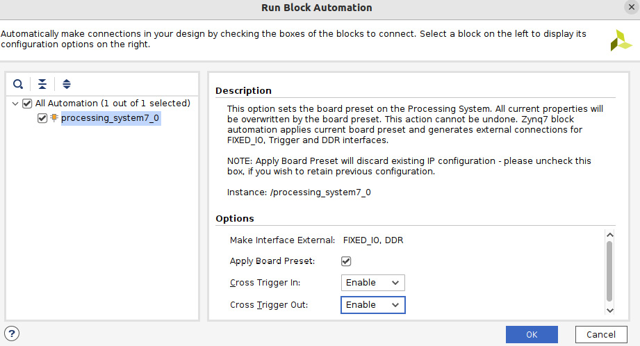
Figure 2.6 – Enabling the PS Trigger In and Trigger Out options
- You will notice that Trigger In and Trigger Out have appeared on the PS interface. Click on the Run Connection Automation command, as suggested by the Designer Assistance of the IP Integrator. This will automatically connect the PS back to the SoC with the correct connectivity in place, as shown in the following diagram. With that, we have added the cross-triggering debug feature between the PS and the AXI BRAM controller that’s implemented within the PL of the Zynq-7000 FPGA:
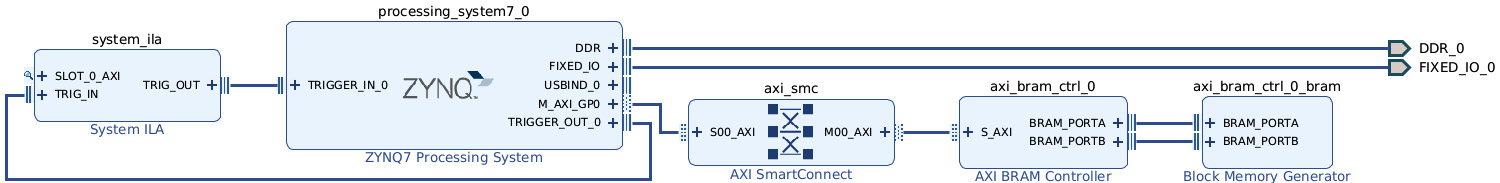
Figure 2.7 – Cross-triggering debug capability
- Now, let’s generate the HDL for this SoC design, which includes the hardware cross-trigger for runtime debugging. At this point, we can check that the design capture is fine by running the Design Rules Check (DRC). Go to the Vivado IDE’s main menu and click on Tools | Validate Design.
FPGA SoC software design flow and associated tools
Software development for an FPGA-based SoC is almost parallel in the SoC’s system design to the FPGA SoC’s hardware platform design. Once the SoC hardware has been fully captured and verified within Vivado, the software development environment can be handed over. This is another advantage of using an FPGA-based SoC compared to an ASIC where you need to either have an emulation version (and usually a costly one) that targets an FPGA-based prototyping platform or have built a system model for virtual prototyping.
There are handover files that the Vivado IDE creates to use as a base platform for the Xilinx software design environment. This chapter will illustrate all these steps, the files involved, as well as the software utilities used to progress the SoC software development, profiling, and debugging phases.
Xilinx’s embedded software development environment is called Vitis. It is the second IDE that centralizes the software building process and manages it as a project.
The Vitis IDE is part of the Vitis unified software platform. The Vitis IDE requires SoC hardware designs built using the Xilinx Vivado IDE. It is based on Eclipse and preserves the familiarity that software developers are acquainted with when building embedded software for discrete microcontrollers. The Vitis IDE’s features include the following:
- Project management and source code version control
- C/C++ code editor
- Compilation environment
- Command-line interface
- Application build configuration and automatic Makefile generation
- Error navigation
- An integrated environment with profiles for debugging and profiling
- System-level performance analysis
- Processor Boot Image generation and Flash programming utilities
- FPGA-specific configuration tools
Vitis IDE embedded software design flow overview
The following diagram shows the embedded software application development steps within the Vitis IDE:

Figure 2.8 – Xilinx Vitis embedded software development steps
Once the hardware design has been completed in the Vivado IDE, the information that’s required by the embedded software development is exported from the Vivado IDE to an XSA archive file. The Vitis IDE imports the XSA archive and creates a platform.
The Vitis platform includes the hardware specification and the software environment settings, which are called a domain. The software developer creates applications based on the platform and domains. The software applications can be debugged in the Vitis IDE. Furthermore, in a complex FPGA SoC that encompasses multiple CPU clusters with multiple cores, several applications may run concurrently while employing some type of inter-process communication (IPC), such as requiring SoC system-level verification. Once all these steps are satisfactory and the SoC FPGA bitstream has been produced within the Vivado environment, the Vitis IDE is used to prepare the boot images that initialize the system and launch the built software applications.
Vitis IDE embedded software design terminology
Before delving into the embedded software design in the following chapters, it is a good idea to become familiar with the main terminology used in this book and across the Xilinx literature related to the FPGA SoC embedded software development flow:
- Workspace: This is the Eclipse IDE framework. When the Vitis environment is launched for the first time, a workspace is created. It is simply a directory that’s used by the Vitis software platform to store project data and metadata.
- XSA: This is the hardware design archive that’s exported from the Vivado Design Suite. It contains hardware specifications such as the processor configuration properties, the peripheral connection information, the system address map, and the device initialization code.
- Platform: The platform is a combination of hardware components and software components. Software components include the Board Support Package (BSP) and the boot components.
- Domain: A domain combines a BSP or the operating system (OS) with a collection of software drivers. A domain is a base for building the user application. We can create multiple applications to run on a specific domain. A domain is tied to a single processor or a cluster of multiple similar CPU cores in the platform.
- System Project: A system project groups applications that run simultaneously on a device. Two bare-metal software applications for the same processor cannot both reside in a system project, whereas two Linux software applications can.
Vitis IDE embedded software design steps
As illustrated in Figure 2.8, first, the hardware design is created with the Vivado IDE. Then, it is exported via the XSA archive file to be used by the Vitis IDE. The software to be run on the FPGA SoC is created step by step, as follows:
- The platform project is created using the XSA file.
- The domain is created and added to a platform project.
- The domain is configured.
- The application is created.
- The application is built (compiled).
- The application is downloaded to the target board (or virtual prototype).
- The application is debugged and profiled.
We will cover the preceding steps on many of the SoC hardware platforms we will be building in the upcoming chapters.
Summary
In this chapter, we introduced the FPGA and SoC hardware design flow, from defining the architecture and capturing it to generating the FPGA device configuration file. We also looked at the hardware design verification that’s involved at every step of the design flow and explained its purpose and how it can be performed. Then, we looked at the SoC design capture in the Vivado IDE and how easily a PS SoC can be created, and how it can be extended using off-the-shelf IPs from the Xilinx IP catalog. We also looked at how hardware and software co-debugging capabilities can be added to the design using the ARM CTI and Xilinx ILA features. We also introduced the SoC software design framework and the Vitis IDE and how a software project can be created using the XSA archive file. Finally, we explored the software design steps and the Xilinx terminology that’s used for the FPGA SoC-embedded software development.
The next chapter will address more of the SoC design and architecture fundamentals, such as the major on-chip interconnect protocols used in modern SoCs, the on-chip data movement, which uses DMA engines, and the data-sharing challenges.
Questions
Answer the following questions to test your knowledge of this chapter:
- List and describe the main steps in the FPGA SoC hardware design flow.
- List and describe the main steps in the FPGA SoC hardware design verification process.
- What are the main elements and features that are used to enable SoC hardware and software co-debugging?
- How important is the co-debugging capability for modern deeply integrated SoCs?
- How many phases are involved in an FPGA SoC design capture? List them and provide a summary of each phase.
- Describe the FPGA SoC software design flow.
- Which design environment is used for designing the software of a Xilinx FPGA-based SoC?
- List the main steps in a Xilinx FPGA SoC-embedded software development flow.