
Chapter 8. Voltage Feedback Op Amp Compensation
Ron Mancini
8.1. Introduction
Voltage feedback amplifiers (VFA) have been with us for about 60 years, and they have been problems for circuit designers since the first day. You see, the feedback that makes them versatile and accurate also has a tendency to make them unstable. The operational amplifier (op amp) circuit configuration uses a high gain amplifier whose parameters are determined by external feedback components. The amplifier gain is so high that, without these external feedback components, the slightest input signal would saturate the amplifier output. The op amp is in common usage, so this configuration is examined in detail, but the results are applicable to many other voltage feedback circuits. Current feedback amplifiers (CFA) are similar to VFAs, but the differences are important enough to warrant handling CFAs separately.
Stability, as used in electronic circuit terminology, is often defined as achieving a nonoscillatory state. This is a poor, inaccurate definition of the word. Stability is a relative term, and this situation makes people uneasy, because relative judgments are exhaustive. It is easy to draw the line between a circuit that oscillates and one that does not oscillate, so we can understand why some people believe that oscillation is a natural boundary between stability and instability.
Feedback circuits exhibit poor phase response, overshooting, and ringing long before oscillation occurs; and these effects are considered undesirable by circuit designers. This chapter is not concerned with oscillators; therefore relative stability is defined in terms of performance. By definition, when designers decide what trade-offs are acceptable, they determine what the relative stability of the circuit is. A relative stability measurement is the damping ratio (ζ). The damping ratio is related to the phase margin, hence the phase margin is another measure of relative stability. The most stable circuits have the longest response times, lowest bandwidth, highest accuracy, and least overshoot. The least stable circuits have the fastest response times, highest bandwidth, lowest accuracy, and some overshoot.
Op amps left in their native state oscillate without some form of compensation. The first IC op amps were very hard to stabilize, but there were a lot of good analog designers around in the 1960s, so we used them. Internally compensated op amps were introduced in the late 1960s in an attempt to make op amps easy for everyone to use. Unfortunately, internally compensated op amps sacrifice a lot of bandwidth and still oscillate under some conditions, so an understanding of compensation is required to apply op amps.
Internal compensation provides a worst case trade-off between stability and performance. Uncompensated op amps require more attention, but they can do more work. Both are covered here.
Compensation is a process of applying a judicious patch in the form of an RC network to make up for a less than perfect op amp or circuit. Many problems can introduce instability, hence there are many compensation schemes.
8.2. Internal Compensation
Op amps are internally compensated to save external components and enable their use by less knowledgeable people. It takes some measure of analog knowledge to compensate an analog circuit. Internally compensated op amps normally are stable when they are used in accordance with the application's instructions. Internally compensated op amps are not unconditionally stable. They are multiple pole systems, but they are internally compensated such that they appear as a single pole system over much of the frequency range. Internal compensation severely decreases the possible closed loop bandwidth of the op amp.
Internal compensation is accomplished in several ways, but the most common method is to connect a capacitor across the collector base junction of a voltage gain transistor (see Figure 8.1). The Miller effect multiplies the capacitor value by an amount approximately equal to the stage gain, thus the Miller effect uses small value capacitors for compensation.
 |
| Figure 8.1 Miller effect compensation. |
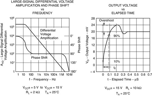
Figure 8.2 shows the gain/phase diagram for an older op amp (TL03X). When the gain crosses the 0 dB axis (gain = 1), the phase shift is approximately 108°, therefore the op amp must be modeled as a second order system because the phase shift is more than 90°.
 |
| Figure 8.2 TL03X frequency and time response plots. |
This yields a phase margin of φ = 180° – 108° = 72°, so the circuit should be very stable. Referring to Figure 8.3, the damping ratio is 1 and the expected overshoot is 0. Figure 8.2 shows approximately 10% overshoot, which is unexpected, but inspecting Figure 8.2 further reveals that the loading capacitance for the two plots is different. The pulse response is loaded with 100 pF rather than the 25 pF shown for the gain/phase plot, and this extra loading capacitance accounts for the loss of phase margin.
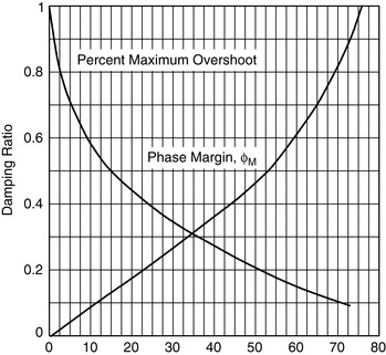 |
| Figure 8.3 Phase margin and percent overshoot versus damping ratio. |
Why does the loading capacitance make the op amp unstable? Look closely at the gain/phase response between 1 MHz and 9 MHz, and observe that the gain curve changes slope drastically while the rate of phase change approaches 120°/decade. The radical gain/phase slope change proves that several poles are located in this area. The loading capacitance works with the op amp output impedance to form another pole, and the new pole reacts with the internal op amp poles. As the loading capacitor value is increased, its pole migrates down in frequency, causing more phase shift at the 0 dB crossover frequency. The proof of this is given in the TL03X data sheet, where plots of ringing and oscillation versus loading capacitance are shown.
Figure 8.4 shows similar plots for the TL07X, which is the newer family of op amps. Note that the phase shift is approximately 100° when the gain crosses the 0 dB axis. This yields a phase margin of 80°, which is close to unconditionally stable. The slope of the phase curve changes to 180°/decade about one decade from the 0 dB crossover point. The radical slope change causes suspicion about the 90° phase margin; furthermore the gain curve must be changing radically when the phase is changing radically. The gain/phase plot may not be totally false, but it sure is overly optimistic.
 |
| Figure 8.4 TL07X frequency and time response plots. |
The TL07X pulse response plot shows approximately 20% overshoot. No loading capacitance is indicated on the plot to account for a seemingly unconditionally stable op amp exhibiting this large an overshoot. Something is wrong here: The analysis is wrong, the plots are wrong, or the parameters are wrong. Figure 8.5 shows the plots for the TL08X family of op amps, which are sisters to the TL07X family. The gain/phase curve and pulse response is virtually identical, but the pulse response lists a 100 pF loading capacitor. This little exercise illustrates three valuable points: First, if the data seem wrong, they probably are wrong; second, even the factory people make mistakes; and third, the loading capacitor makes op amps ring, overshoot, or oscillate.
 |
| Figure 8.5 TL08X frequency and time response plots. |
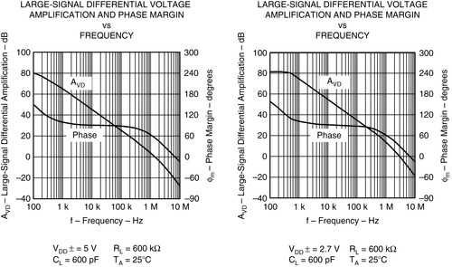
The frequency and time response plots for the TLV277X family of op amps is shown in Figure 8.6 and Figure 8.7. First, note that the information is more sophisticated because the phase response is given in degrees of phase margin; second, both gain/phase plots are done with substantial loading capacitors (600 pF), so they have some practical value; and third, the phase margin is a function of power supply voltage.
 |
| Figure 8.6 TLV277X frequency response plots. |
 |
| Figure 8.7 TLV277X time response plots. |
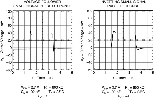
At VCC = 5 V, the phase margin at the 0 dB crossover point is 60°, while it is 30° at VCC = 2.7 V. This translates into an expected overshoot of 18% at VCC = 5 V and 28% at VCC = 2.7 V. Unfortunately the time response plots are done with 100 pF loading capacitance, hence we cannot check our figures very well. The VCC = 2.7 V overshoot is approximately 2%, and it is almost impossible to figure out what the overshoot would have been with a 600 pF loading capacitor. The small signal pulse response is done with millivolt signals, and that is a more realistic measurement than using the full signal swing.
Internally compensated op amps are very desirable because they are easy to use and do not require external compensation components. Their drawback is that the bandwidth is limited by the internal compensation scheme. The op amp open loop gain eventually (when it shows up in the loop gain) determines the error in an op amp circuit. In a noninverting buffer configuration, the TLV277X is limited to 1% error at 50 kHz (VCC = 2.7 V) because the op amp gain is 40 dB at that point. Circuit designers can play tricks, such as bypassing the op amp with a capacitor to emphasize the high frequency gain, but the error is still 1%. Keep Equation (8.1) in mind, because it defines the error. If the TLV277X were not internally compensated, it could be externally compensated for a lower error at 50 kHz, because the gain would be much higher.
(8.1)
8.3. External Compensation, Stability, and Performance
Nobody compensates an op amp just because it is there; designers have a reason to compensate the op amp, and that reason is usually stability. They want the op amp to perform a function in a circuit where it is potentially unstable. Internally and noninternally compensated op amps are compensated externally because certain circuit configurations do cause oscillations. Several potentially unstable circuit configurations are analyzed in this section, and the reader can extend the external compensation techniques as required.
Other reasons for externally compensating op amps are noise reduction, flat amplitude response, and obtaining the highest bandwidth possible from an op amp. An op amp generates noise, and noise is generated by the system. The noise contains many frequency components; and when a high pass filter is incorporated in the signal path, it reduces high frequency noise. Compensation can be employed to roll off the op amp's high frequency, closed loop response, thus causing the op amp to act as a noise filter. Internally compensated op amps are modeled with a second order equation, and this means that the output voltage can overshoot in response to a step input. When this overshooting (or peaking) is undesirable, external compensation can increase the phase margin to 90°, where there is no peaking. An uncompensated op amp has the highest bandwidth possible. External compensation is required to stabilize uncompensated op amps, but the compensation can be tailored to the specific circuit, thus yielding the highest possible bandwidth consistent with the pulse response requirements.
8.4. Dominant Pole Compensation
We saw that capacitive loading caused potential instabilities, therefore an op amp loaded with an output capacitor is a circuit configuration that must be analyzed. This circuit is called dominant pole compensation, because if the pole formed by the op amp output impedance and the loading capacitor is located close to the zero frequency axis, it becomes dominant. The op amp circuit is shown in Figure 8.8 and the open loop circuit used to calculate the loop gain (Aβ) is shown in Figure 8.9.
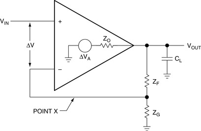 |
| Figure 8.8 Capacitively loaded op amp. |
 |
| Figure 8.9 Capacitively loaded op amp with loop broken for loop gain (Aβ) calculation. |
The analysis starts by looking into the capacitor and taking the Thevenin equivalent circuit: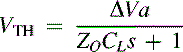

(8.2)
(8.3)
Then, the output equation is written: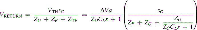
(8.4)
Rearranging terms yields Equation (8.5):
(8.5)
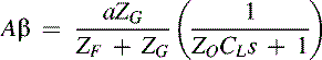
Equation (8.7) models the op amp as a second order system. Hence, substituting the second order model for a in Equation (8.6) yields Equation (8.8), which is the stability equation for the dominant pole compensation circuit: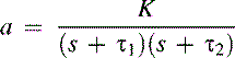

(8.7)
(8.8)
Several conclusions can be drawn from Equation (8.8), depending on the location of the poles. If the Bode plot of Equation (8.7), the op amp transfer function, looks like that shown in Figure 8.10, it has only a 25° phase margin and there is approximately a 48% overshoot. When the pole introduced by ZO and CL moves toward the zero frequency axis, it comes close to the τ2 pole, and it adds phase shift to the system. Increased phase shift increases peaking and decreases stability. In the real world, many loads, especially cables, are capacitive; and an op amp like the one pictured in Figure 8.10 would ring while driving a capacitive load. The load capacitance causes peaking and instability in internally compensated op amps when the op amps do not have enough phase margin to allow for the phase shift introduced by the load.
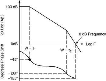 |
| Figure 8.10 Possible Bode plot of the op amp described in Equation (8.7). |
Prior to compensation, the Bode plot of an uncompensated op amp looks like that shown in Figure 8.11. Note that the break points are located close together, accumulating about 180° of phase shift before the 0 dB crossover point; the op amp is not usable and probably unstable. Dominant pole compensation is often used to stabilize these op amps. If a dominant pole, in this case ωD, is properly placed, it rolls off the gain so that τ1 introduces 45° phase at the 0 dB crossover point. After the dominant pole is introduced, the op amp is stable with 45° phase margin, but the op amp gain is drastically reduced for frequencies higher than ωD. This procedure works well for internally compensated op amps but is seldom used for externally compensated op amps, because inexpensive discrete capacitors are readily available.
 |
| Figure 8.11 Dominant pole compensation plot. |
Assuming that ZO ≪ ZF, the closed loop transfer function is easy to calculate, because CL is enclosed in the feedback loop. The ideal closed loop transfer equation is the same as Equation (7.11) for the noninverting op amp and is repeated here as Equation (8.9):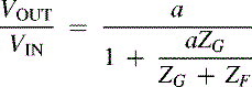
(8.9)

As long as the op amp has enough compliance and current to drive the capacitive load and ZO is small, the circuit functions as though the capacitor were not there. When the capacitor becomes large enough, its pole interacts with the op amp pole, causing instability. When the capacitor is huge, it completely kills the op amp's bandwidth, thus lowering the noise while retaining a large low frequency gain.
8.5. Gain Compensation
When the closed loop gain of an op amp circuit is related to the loop gain, as it is in voltage feedback op amps, the closed loop gain can be used to stabilize the circuit. This type of compensation cannot be used in current feedback op amps because a mathematical relationship between the loop gain and ideal closed loop gain does not exist. The loop gain equation is repeated as Equation (8.11). Note that the closed loop gain parameters ZG and ZF are contained in Equation (8.11); hence the stability can be controlled by manipulating the closed loop gain parameters: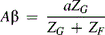
(8.11)
The original loop gain curve for a closed loop gain of 1 is shown in Figure 8.12 and it is or comes very close to being unstable. If the closed loop noninverting gain is changed to 9, then K changes from K/2 to K/10. The loop gain intercept on the Bode plot (Figure 8.12) moves down 14 dB and the circuit is stabilized.
 |
| Figure 8.12 Gain compensation. |
Gain compensation works for inverting or noninverting op amp circuits, because the loop gain equation contains the closed loop gain parameters in both cases. When the closed loop gain is increased, the accuracy and bandwidth decrease. As long as the application can stand the higher gain, gain compensation is the best type of compensation to use. Uncompensated versions of normally internally compensated op amps are offered for sale as stable op amps with minimum gain restrictions. As long as gain in the circuit designed exceeds the gain specified on the data sheet, this is economical and a safe mode of operation.
8.6. Lead Compensation
Sometimes lead compensation is forced on the circuit designer because of the parasitic capacitance associated with packaging and wiring op amps. Figure 8.13 shows the circuit for lead compensation; note the capacitor in parallel with RF. That capacitor is often made by parasitic wiring and the ground plane, and high frequency circuit designers go to great lengths to minimize or eliminate it. What is good in one sense is bad in another, because adding the parallel capacitor is a good way to stabilize the op amp and reduce noise. Let's analyze the stability first, then we analyze the closed loop performance.
 |
| Figure 8.13 Lead compensation circuit. |
The loop equation for the lead compensation circuit is given by Equation (8.12):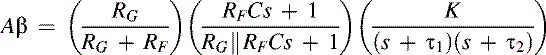
(8.12)
The compensation capacitor introduces a pole and zero into the loop equation. The zero always occurs before the pole because RF > RF‖RG. When the zero is properly placed, it cancels out the τ2 pole along with its associated phase shift. The original transfer function is shown in Figure 8.14, drawn in solid lines. When the RFC zero is placed at ω = 1/τ2, it cancels out the τ2 pole, causing the Bode plot to continue on a slope of −20 dB/decade. When the frequency gets to ω = 1/(RF‖RG)C, this pole changes the slope to −40 dB/decade. Properly placed, the capacitor aids stability, but what does it do to the closed loop transfer function? The equation for the inverting op amp closed-loop gain is repeated here:
(8.13)
 |
| Figure 8.14 Lead compensation Bode plot. |

Substituting RF‖C for ZF and RG for ZG in Equation (8.14) yields Equation (8.15), which is the ideal closed loop gain equation for the lead compensation circuit:
(8.15)
The forward gain for the inverting amplifier is given by Equation (8.16). Compare Equation (8.13) with Equation (6.5) to determine A: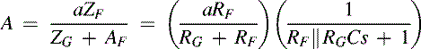
(8.16)
The op amp gain (a), the forward gain (A), and the ideal closed loop gain are plotted in Figure 8.15. The op amp gain is plotted for reference only. The forward gain for the inverting op amp is not the op amp gain. Note that the forward gain is reduced by the factor RF/(RG + RF), and it contains a high frequency pole. The ideal closed loop gain follows the ideal curve until the 1/RFC break point (same location as 1/τ2 break point), then it slopes down at −20 dB/decade. Lead compensation sacrifices the bandwidth between the 1/RFC break point and the forward gain curve. The location of the 1/RFC pole determines the bandwidth sacrifice, and it can be much greater than shown here. The pole caused by RF, RG, and C does not appear until the op amp's gain has crossed the 0 dB axis, thus it does not affect the ideal closed loop transfer function.
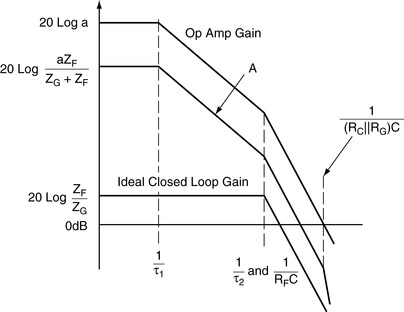 |
| Figure 8.15 Inverting op amp with lead compensation. |
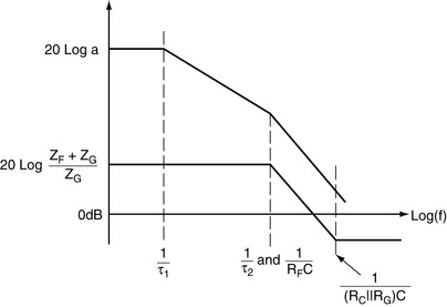
The forward gain for the noninverting op amp is a; compare Equation (7.11) and Equation (7.5). The ideal closed loop gain is given by Equation (8.17):
(8.17)
The plot of the noninverting op amp with lead compensation is shown in Figure 8.16. There is only one plot for both the op amp gain (a) and the forward gain (A), because they are identical in the noninverting circuit configuration. The ideal starts out as a flat line, but it slopes down because its closed loop gain contains a pole and a zero. The pole always occurs closer to the low frequency axis, because RF > RF‖RG. The zero flattens the ideal closed loop gain curve, but it never does any good because it cannot fall on the pole. The pole causes a loss in the closed loop bandwidth by the amount separating the closed loop and forward gain curves.
 |
| Figure 8.16 Noninverting op amp with lead compensation. |
Although the forward gain is different in the inverting and noninverting circuits, the closed loop transfer functions take very similar shapes. This becomes truer as the closed loop gain increases because the noninverting forward gain approaches the op amp gain. This relationship cannot be relied on in every situation, and each circuit must be checked to determine the closed loop effects of the compensation scheme.
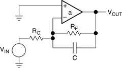
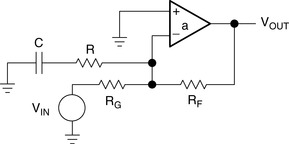
8.7. Compensated Attenuator Applied to Op Amp
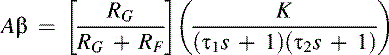
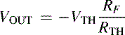
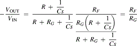
Stray capacitance on op amp inputs is a problem that circuit designers are always trying to avoid, because it decreases stability and causes peaking. The circuit shown in Figure 8.17 has some stray capacitance (CG) connected from the inverting input to ground. Equation (8.18) is the loop gain equation for the circuit with input capacitance:
(8.18)
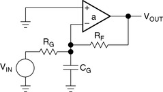 |
| Figure 8.17 Op amp with stray capacitance on the inverting input. |
Op amps having high input and feedback resistors are subject to instability caused by stray capacitance on the inverting input. Referring to Equation (8.18), when the 1/(RF‖RGCG) pole moves close to τ2, the stage is set for instability. Reasonable component values for a CMOS op amp are RF = 1 MΩ, RG = 1 MΩ, and CG = 10 pF. The resulting pole occurs at 318 kHz, and this frequency is lower than the break point of τ2 for many op amps. A 90° of phase shift results from τ1, the 1/(RF‖RGC) pole adds 45° phase shift at 318 kHz, and τ2 starts to add another 45° phase shift at about 600 kHz. This circuit is unstable because of the stray input capacitance. The circuit is compensated by adding a feedback capacitor, as shown in Figure 8.18.
 |
| Figure 8.18 Compensated attenuator circuit. |
The loop gain with CF added is given by Equation (8.19):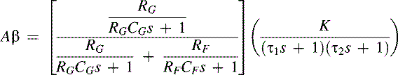
(8.19)
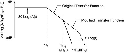
The compensated attenuator Bode plot is shown in Figure 8.19. Adding the correct 1/RFCF break point cancels out the 1/RGCG break point; the loop gain is independent of the capacitors. Now is the time to take advantage of the stray capacitance. CF can be formed by running a wide copper strip from the output of the op amp over the ground plane under RF; do not connect the other end of this copper strip. The circuit is tuned by removing some copper (a razor works well) until all peaking is eliminated. Then, measure the copper and have an identical trace put on the printed circuit board.
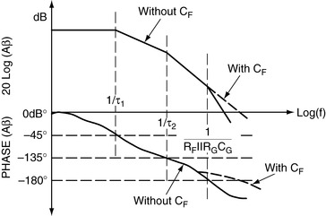 |
| Figure 8.19 Compensated attenuator Bode plot. |
The inverting and noninverting closed loop gain equations are a function of frequency. Equation (8.21) is the closed loop gain equation for the inverting op amp. When RFCF = RGCG, Equation (8.21) reduces to Equation (8.22), which is independent of the break point. This also happens to the noninverting op amp circuit. This is one of the few occasions when the compensation does not affect the closed loop gain frequency response.
(8.21)
When RFCF = RGCG,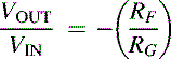
(8.22)
8.8. Lead/Lag Compensation
Lead/lag compensation stabilizes the circuit without sacrificing the closed loop gain performance. It is often used with uncompensated op amps. This type of compensation provides excellent high frequency performance. The circuit schematic is shown in Figure 8.20 and the loop gain is given by Equation (8.23):
(8.23)
 |
| Figure 8.20 Lead/lag compensated op amp. |
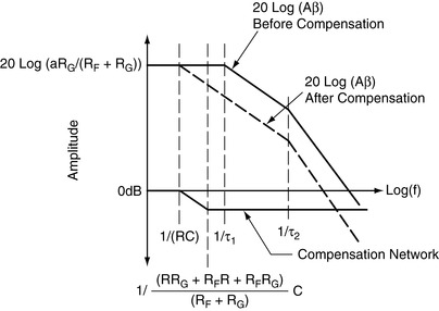
Referring to Figure 8.21, a pole is introduced at ω = 1/RC, and this pole reduces the gain 3 dB at the break point. When the zero occurs prior to the first op amp pole, it cancels out the phase shift caused by the ω = 1/RC pole. The phase shift is completely canceled before the second op amp pole occurs, and the circuit reacts as if the pole were never introduced. Nevertheless, Aβ is reduced by 3 dB or more, so the loop gain crosses the 0 dB axis at a lower frequency. The beauty of lead/lag compensation is that the closed loop ideal gain is not affected, as is shown next. The Thevenin equivalent of the input circuit is calculated in Equation (8.24), the circuit gain in terms of Thevenin equivalents is calculated in Equation (8.25) and the ideal closed loop gain is calculated in Equation (8.26):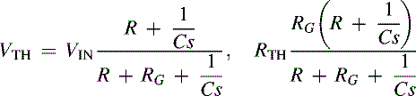
(8.24)
(8.25)
(8.26)
 |
| Figure 8.21 Bode plot of lead/lag compensated op amp. |
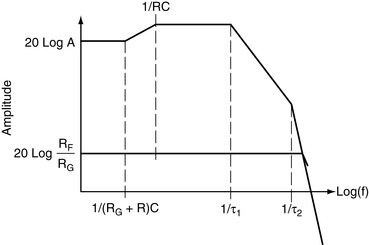
Equation (8.26) is intuitively obvious, because the RC network is placed across a virtual ground. As long as the loop gain, Aβ, is large, the feedback nulls out the closed loop effect of RC and the circuit will function as if it were not there. The closed loop log plot of the lead/lag compensated op amp is given in Figure 8.22. Note that the pole and zero resulting from the compensation occur and are gone before the first amplifier poles come on the scene. This prevents interaction, but it is not required for stability.
 |
| Figure 8.22 Closed loop plot of lead/lag compensated op amp. |
8.9. Comparison of Compensation Schemes
Internally compensated op amps can, and often do, oscillate under some circuit conditions. Internally compensated op amps need an external pole to get the oscillation or ringing started, and circuit stray capacitances often supply the phase shift required for instability. Loads, such as cables, often cause internally compensated op amps to ring severely.
Dominant pole compensation is often used in IC design because it is easy to implement. It rolls off the closed loop gain early; therefore it is seldom used as an external form of compensation unless filtering is required. Load capacitance, depending on its pole location, usually causes the op amp to ring. Large load capacitance can stabilize the op amp because it acts as dominant pole compensation.
The simplest form of compensation is gain compensation. High closed loop gains are reflected in lower loop gains, and, in turn, lower loop gains increase stability. If an op amp circuit can be stabilized by increasing the closed loop gain, do it.
Stray capacitance across the feedback resistor tends to stabilize the op amp because it is a form of lead compensation. This compensation scheme is useful for limiting the circuit bandwidth, but it decreases the closed loop gain.
Stray capacitance on the inverting input works with the parallel combination of the feedback and gain setting resistors to form a pole in the Bode plot, and this pole decreases the circuit's stability. This effect is normally observed in high impedance circuits built with CMOS op amps. Adding a feedback capacitor forms a compensated attenuator scheme that cancels out the input pole. The cancellation occurs when the input and feedback RC time constants are equal. Under the conditions of equal time constants, the op amp functions as though the stray input capacitance were not there. An excellent method of implementing a compensated attenuator is to build a stray feedback capacitor using the ground plane and a trace off the output node.
Lead/lag compensation stabilizes the op amp, and it yields the best closed loop frequency performance. Contrary to some published opinions, no compensation scheme increases the bandwidth beyond that of the op amp. Lead/lag compensation just gives the best bandwidth for the compensation.
8.10. Conclusions
The stability criteria often is not oscillation, rather it is circuit performance as exhibited by peaking and ringing.
The circuit bandwidth can often be increased by connecting an external capacitor in parallel with the op amp. Some op amps have hooks that enable a parallel capacitor to be connected in parallel with a portion of the input stages. This increases bandwidth because it shunts high frequencies past the low bandwidth gm stages, but this method of compensation depends on the op amp type and manufacturer.
The compensation techniques given here are adequate for the majority of applications. When the new and challenging application presents itself, use the procedure outlined here to invent your own compensation technique.
..................Content has been hidden....................
You can't read the all page of ebook, please click here login for view all page.