
Chapter 18. Interfacing DACs to Loads
Bruce Carter
18.1. Introduction
A digital to analog converter, DAC, is a component that takes a digital word and converts it to a corresponding analog voltage. It has the opposite function of an analog to digital converter. The DAC is capable of producing only a quantized representation of an analog voltage, not an infinite range of output voltages.
The application almost always dictates the selection of the DAC, leaving the designer the task of interfacing that converter with the output load.
A DAC interfaces with a buffer op amp. Most DACs are manufactured with a process that is incompatible with op amps. Therefore, the op amp cannot be manufactured on the same IC. It must be external, and its characteristics are an integral part of the conversion process. In most cases, the data sheet makes a recommendation for the selection of a buffer op amp. Follow the recommendation, unless there is a compelling reason not to do so. Performance can be improved only if you know exactly what op amp specifications need to be optimized.
All signal conditioning—low pass filtering, DC offsets, and power stages—should be placed after the recommended op amp buffer. Do not attempt to combine these functions with the buffer unless you are an experienced designer with a good grasp of all of the implications.
18.2. Load Characteristics
There are two main types of loads that a DAC may have to drive, AC and DC. Each has different characteristics and requires different interface circuitry.
18.2.1. DC Loads
DC loads include linear actuators such as those used on positioning tables, motors, programmable power supplies, outdoor displays, and lighting systems. Large load currents or high voltages characterize some of these loads. DC accuracy is important, because it is related to a series of desired mechanical positions or intensities in the load device.
18.2.2. AC Loads
AC loads include things like audio chains, frequency generators, IF outputs—any load that does not have a DC component.
18.3. Understanding the DAC and Its Specifications
It is important to understand the DAC and its specifications before discussing interfaces.
18.3.1. Types of DACs—Understanding the Trade-Offs
DACs are available in several types, the most common of which is the resistor ladder type. There are several variations on the resistor ladder technique, with the R/2R configuration being the most common.
18.3.2. The Resistor Ladder DAC
In the resistor ladder DAC, a precision voltage reference is divided into 2N−1 parts in an internal voltage divider, where N is the number of bits specified for the converter. One switch at a time turns on, corresponding to the correct DC level (Figure 18.1).
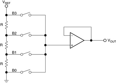 |
| Figure 18.1 Resistor ladder DAC. |
Unfortunately, the number of resistors and switches doubles for each additional bit of resolution. This means that an 8 bit DAC has 255 resistors and 256 switches, and a 16 bit DAC has 65,535 resistors and 65,536 switches. For this reason, this architecture is almost never used for higher resolution DACs.
18.3.3. The Weighted Resistor DAC
The weighted resistor DAC is very similar to the resistor ladder DAC. In this case, however, each resistor in the string is given a value proportional to the binary value of the bit it represents. Currents are then summed from each active bit to achieve the output (Figure 18.2).
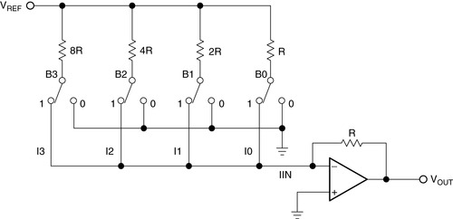 |
| Figure 18.2 Binary weighted DAC. |
The number of resistors and switches are reduced to one per bit, but the range of the resistors is extremely wide for high resolution converters, making it hard to fabricate all of them on the IC. The resistor used for B0 in Figure 18.2 is the limiting factor for power dissipation from VREF to ground.
This converter architecture is often used to make logarithmic converters. In this case, the R, 2R, 4R, 8R, … resistors are replaced with logarithmically weighted resistors.
This type of converter and the R/2R converter described in the next subsection use a feedback resistor fabricated on the DAC IC itself. This feedback resistor is not an optional convenience for the designer—it is crucial to the accuracy of the DAC. It is fabricated on the same silicon as the resistor ladder. Therefore, it experiences the same thermal drift as the resistor ladder. The gain of the buffer amplifier is fixed, with a full scale output voltage limited to VREF. If a different full scale DAC output voltage is needed, change VREF. If the full scale VOUT must exceed the maximum rating of the DAC reference voltage, use a gain stage after the buffer op amp (see Section 18.7.2).
The op amp must be selected carefully, because it is operated in much less than unity gain mode for some combinations of bits. This is probably one of the main reasons why this architecture is not popular, as well as the requirement for a wide range of resistor values for high precision converters.
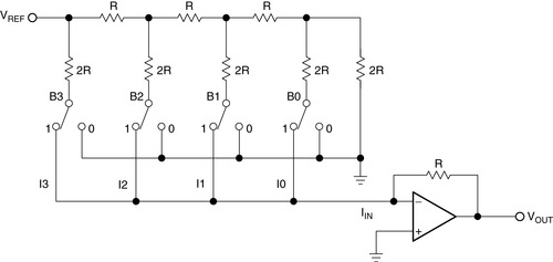
18.3.4. The R/2R DAC
An R/2R network can be used to make a DAC that has none of the disadvantages of the types mentioned previously (Figure 18.3).
 |
| Figure 18.3 R/2R resistor array. |
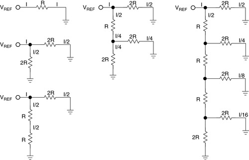
For a given reference voltage, VREF, a current I flows through resistor R. If two resistors, each the same value (2R) are connected from VREF to ground, a current I/2 flows through each leg of the circuit. But the same current flows if one leg is made up of two resistors, each with the value of R. If two resistors in parallel whose value is 2R replace the bottom resistor, the parallel combination is still R. I/4 flows through both legs, adding to I/2. Extending the network for 4 bits as shown on the right, the total current on the bottom leg is I/4 plus I/8 plus I/16 plus I/16 in the resistor to ground. Kirchhoff's current law is satisfied and convenient tap points have been established to construct a DAC (Figure 18.4).
 |
| Figure 18.4 R/2R DAC. |
This converter architecture has advantages over the types previously mentioned. The number of resistors has doubled from the number required for the current summing type, but there are only two values. Usually, the 2R resistors are composed of two resistors in series, each with a value of R. The feedback resistor for the buffer amplifier is again fabricated on the converter itself for maximum accuracy. Although the op amp is still not operated in unity gain mode for all combinations of bits, it is much closer to unity gain with this architecture.
The important op amp parameters for all resistor ladder DACs are
• Input offset voltage—the lower the better. It adds to the converter offset error.
• Input bias current—the lower the better. The product of the bias current and the feedback resistance creates an output offset error.
• Output voltage swing—it must meet or, preferably, exceed the zero to full scale swing from the DAC.
• Settling time and slew rate—it must be fast enough to allow the op amp to settle before the next digital bit combination is presented to the DAC input register.
18.3.5. The Sigma Delta DAC
The sigma delta DAC takes advantage of the speed of advanced IC processes to do a conversion as a series of approximations summed together. A phase locked loop (PLL) derived sample clock operates at many times the overall conversion frequency; in the case shown in Figure 18.5, it is 128×. The PLL is used to drive an interpolation filter, a digital modulator, and a 1 bit DAC. The conversion is done by using the density ratio of the voltage out of the 1 bit DAC as the analog signal. As the pattern of ones and zeros is presented to the 1 bit converter, their time average at the sample frequency recreates the analog waveform.
 |
| Figure 18.5 Sigma delta DAC. |
Sigma delta converters are popular for audio frequencies, particularly CD players. The primary limiting factor is the sample clock. CD players operate at a sample rate of 44.1 kHz, which means that, according to Nyquist sampling theory, the maximum audio frequency that can be reproduced is 22.05 kHz. If an audio frequency of 23.05 kHz is present in the recorded material, it will alias back into the audio output at 1 kHz, producing an annoying whistle. This places a tremendous constraint on the low pass filter following the DAC in a CD player. It must reject all audio frequencies above 22.05 kHz while passing those up to 20 kHz, the commonly accepted upper limit of human hearing. While this can be done in conventional filter topologies, they are extremely complex (nine or more poles). Inevitably, phase shift and amplitude roll-off or ripple starts far below 20 kHz. The original CD players often sounded a bit “harsh” or “dull” because of this.
The solution was to overclock the sample clock. To keep things simple, designers made it a binary multiple of the original sampling frequency. Today, eight times or even higher oversampling is standard in CD players. Little do the audio enthusiasts know that the primary reason why this was done was to substantially reduce the cost of the CD player. A faster sample clock is very cheap. Nine pole audio filters are not. At eight times oversampling, the CD player needs to achieve maximum roll-off at only 352.8 kHz, a very easy requirement. Instead of the filter having to roll off in a mere 2 kHz of bandwidth, now it has 332 kHz of bandwidth to accomplish the roll-off. The sound of an oversampled CD player really is better, but it comes at the cost of increased radiated RFI, coming from the sample clock.
Sigma delta converters introduce a great deal of noise onto the power rails, because the internal digital circuitry is continually switching to the power supply rails at the sample clock frequency fS.
18.4. DAC Error Budget
The system designer must do an error budget to know how many bits are actually needed to meet the system requirements—how much “graininess” or what step size is acceptable in the output signal.
18.4.1. Accuracy versus Resolution
It is important for the designer to understand the difference between converter accuracy and converter resolution. The number of bits determines resolution of a converter. Insufficient resolution is not an error—it is a design characteristic of the DAC. If a given converter's resolution is insufficient, use a converter with better resolution (more bits).
Accuracy is the error in the analog output from the theoretical value for a given digital input. Errors are described in the next section. A very common method of compensating for DAC error is to use a converter that has 1 or 2 bits more resolution than the application requires. With the cost of converters coming down and more advanced models being introduced every day, this may be cost effective.
18.4.2. DC Application Error Budget
DC applications depend on the value of DC voltage coming out of the converter. THD and signal to noise ratio are not important, because the frequency coming out of the converter is almost DC.
The resolution of a converter is ±½ LSB, where an LSB is defined as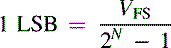 where
where
(18.1)
VFS = Full scale output voltage.
N = Number of converter bits.
The number of bits in a DC system determines the DC step size that corresponds to a bit. Table 18.1 shows the number of bits and the corresponding voltage step size for three popular voltages.
The bit step size can get critical, especially for portable equipment. There is a requirement to operate off of low voltage to minimize the number of batteries. The buffer amplifier, if it includes gain, uses large resistor values, lowering its noise immunity. Fortunately, the vast majority of DC applications are not portable; they are in an industrial environment.
For example, a converter is used to position a drill on a table used to drill PCB holes. The positions of the holes are specified as 0.001 in., ±0.0003 in. The actuators are centered on the table at 0 V, with full negative position of −12 in. occurring at −5 V, and full positive position of +12 in. occurring at +5 V. There are two actuators, one for vertical, and one for horizontal.
This example has several aspects. The first is that the positioning voltage has to swing both positive and negative. In the real world, it may be necessary to add (or subtract in this case) a fixed offset to the DAC output. The output voltage has to swing over a 10 V range, which may mean that the output of the DAC has to be amplified. The actuators themselves probably operate off of higher current than the DAC is designed to provide. Section 18.7 covers some methods for meeting these requirements.
Assume, for now, that the DAC has the necessary offset and gain. A ±12 in. position is 24 in. total, which corresponds to ±5 V from the DAC circuitry. The 24 in. range must be divided into equal 0.0003 in. steps to meet the resolution requirement, which is 80,000 steps. From Table 18.1, an 18 bit DAC is required. The actual system is able to position with a step size of 0.0000916 in. Two independent conversion systems are needed, one for horizontal and one for vertical.
18.4.3. AC Application Error Budget
The error budget for an AC application most likely is specified as total harmonic distortion, dynamic range, or signal to noise ratio. Assuming no internal noise and no noise in the buffer op amp circuitry, the inverse of the dynamic range is the SNR of the DAC. Of course, noise is always present and is measured with all input data set to zero. Noise makes the SNR decrease.
The number of converter bits, however, is the overwhelming factor determining these parameters. Technically, they are not “errors,” because the design of the converter sets them. If the designer cannot live with these design limits, the only choice is to specify a converter with better resolution (more bits).
Total Harmonic Distortion
The total harmonic distortion of an ideal DAC is the quantization noise due to the converter resolution. The number of bits of the converter determines the lowest possible total harmonic distortion. The greater is the number of bits, the lower the amplitude of the harmonics, as shown in Figure 18.6.
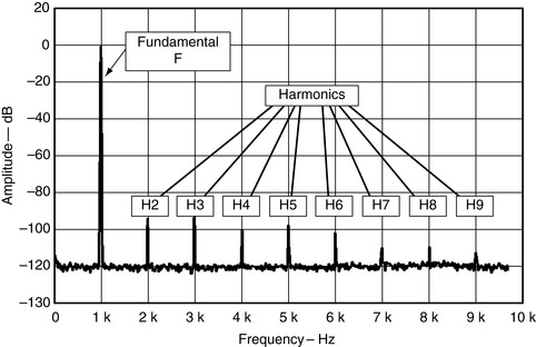 |
| Figure 18.6 Total harmonic distortion. |
Assuming ideal digital to analog conversion, there is a direct relationship between the number of bits and the THD caused by the resolution: where N is the number of converter bits. Of course, this is the limit for ideal conversion.
(18.2)
Dynamic Range
There is also a direct relationship between the number of bits (N) and the maximum dynamic range of the DAC, Equation (18.2) and Table 18.2: Note that there is approximately a 6 dB improvement in dynamic range per bit. This is an easy way to figure out what improvement can be realized by increasing the number of bits from one value to another.
(18.3)
For example, if the designers of a CD player want to have a 90 dB SNR, they would pick a 16 bit converter from Table 18.2. The THD is 0.0015% minimum.
18.4.4. RF Application Error Budget
RF applications are a high frequency subset of AC applications. RF applications may be concerned with the position and relative amplitude of various harmonics. Minimizing one harmonic at the expense of another may be acceptable if the overall RF spectrum is within specified limits.
18.5. DAC Errors and Parameters
The DAC errors described in this section add to the errors caused by the resolution of the converter.
The section is divided into DC and AC sections, but many of the DC errors masquerade as AC errors. A given DAC may or may not include either DC or AC error specifications. This should give the designer a clue that the device is optimized for DC or AC applications. Like any component, DACs are designed with trade-offs. It is possible to misapply a converter meant for high frequency AC operation in a DC application and so forth.
18.5.1. DC Errors and Parameters
The following are some DAC DC errors and parameters.
Offset Error
The analog output voltage range for the complete range of input bits may be shifted linearly from the ideal 0 to the full scale value (Figure 18.7). The offset error is the ±ΔV from 0 V that results when a digital code is entered that is supposed to produce 0.
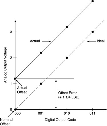 |
| Figure 18.7 DAC offset error. |
Related to the offset error is the offset error temperature coefficient, which is the change in offset over temperature. This is usually specified in pulse position modulation per degree Centigrade.
The offset error is critical in DC applications. For this reason, a buffer op amp must be selected that does not contribute to the problem—its own offset voltages should be much less than that of the converter. In AC applications, the offset error is not important and can be ignored. The buffer op amp can be selected for low THD, high slew rate, or whatever other parameters are important for the application.
Gain Error
The gain of the DAC may greater than or less than the gain needed to produce the desired full scale analog voltage (Figure 18.8). The gain error is the difference in slope between the ideal DAC output gain and the actual gain.
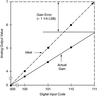 |
| Figure 18.8 DAC gain error. |
Related to the gain error is the gain error temperature coefficient, which is the change in gain over temperature.
The gain error can be critical in both AC and DC applications. For example,
• An RF predriver must not cause the output stage to exceed FCC license requirements.
• A mechanical positioner must not stop short of or go past its intended position.
The op amp buffer should be operated with the internal feedback resistor. If possible, full scale amplitude adjustments should be made to VREF. This way, tolerances and thermal drift in external resistors do not contribute to the gain error.
Differential Nonlinearity Error
When the increase in output voltage (ΔV) is not the same for every combination of bits, the converter has a differential nonlinearity error (DNL). If the DNL exceeds 1 LSB, the converter is nonmonotonic. This can cause a problem for some servo control loops. A nonmonotonic DAC would appear in Figure 18.9 as a momentary dip in the analog output characteristic.
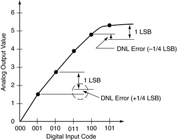 |
| Figure 18.9 Differential nonlinearity error. |
Integral Nonlinearity Error
The integral nonlinearity error is similar to the differential nonlinearity error, except it is a first order effect that stretches across the entire range from 0 to full scale output voltage (Figure 18.10).
 |
| Figure 18.10 Integral nonlinearity error. |
Both the INL and DNL errors affect AC applications as distortion and spectral harmonics (spurs). In DC applications, they result in an error in the DC output voltage. The mechanical steps of a positioning table, for instance, may not be in exact increments.
Power Supply Rejection Ratio
The power supply rejection ratio is sometimes called the power supply sensitivity. It is the ability of the converter to reject ripple and noise on its power inputs. DC applications may not be adversely affected. Poor power supply rejection can cause spurs and harmonic distortion in AC applications, as external frequency components leak into the output and modulate with it. The designer must decouple the DAC and buffer op amp carefully to combat these problems.
18.5.2. AC Errors and Parameters
The following are DAC AC errors and parameters.
THD + N
Some noise is always generated internally in the converter and buffer amp. A useful specification for audio and communication system designers is the THD + N (total harmonic distortion plus noise). The distortion plus noise (THD + N) is the ratio of the sum of the harmonic distortion and noise to the rms power of the input signal. As is the case with op amp parameters (Chapter 13), the noise sources add according to the root mean square law. The distortion and noise are measured separately then added together to form the ratio. The noise voltage relates to the measured bandwidth.
SINAD
The signal to noise and distortion (SINAD) ratio is the ratio of the input signal to the sum of the harmonic distortion and noise. The distortion and noise are measured separately then added together to form the ratio. The SINAD is the reciprocal to the THD + N. The SINAD and THD + N are a good indication of the overall dynamic performance of the ADC, because all components of noise and distortion are included.
ENOB
The SINAD is used to determine the effective number of bits (ENOB) of accuracy the converter displays at that frequency. For example, a nominal 8 bit resolution DAC may be specified as having 45 dB SNR at a particular input frequency. The number of effective bits is defined as 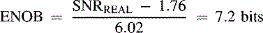
(18.4)
The actual performance of the device is therefore less than its nominal resolution at this frequency.
Spurious Free Dynamic Range
Spurious free dynamic range is the difference in decibels between the maximum signal component and the largest distortion component (Figure 18.11). It is an important specification in RF applications, where FCC regulations specify the magnitude of spurs.
 |
| Figure 18.11 Spurious free dynamic range. |
Improper decoupling may cause spurs. A notch filter can be used to eliminate a spur, but many RF applications are RF agile—changing the frequency of the spur as well. The notch must catch all spur frequencies or it is useless.
Intermodulation Distortion
The differential and integral nonlinearity errors described previously appear in a high frequency AC application as intermodulation distortion (Figure 18.12).
 |
| Figure 18.12 Intermodulation distortion. |
The best method of combating intermodulation distortion is to make the buffer amplifier system as linear as possible (beware of rail to rail op amps that may not be linear near the voltage rails). Try to limit current through the internal feedback resistor in the DAC. See Section 18.7.1 on increasing the voltage rail for suggestions about reducing internal feedback resistor power dissipation.
Settling Time
The settling time of a DAC is the time between the switching of the digital inputs of the converter and when the output reaches its final value and remains within a specified error band (Figure 18.13). Settling time is the reciprocal of the maximum DAC conversion rate.
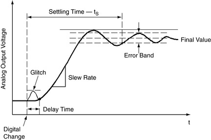 |
| Figure 18.13 DAC settling time. |
When an output buffer op amp is used with a DAC, it becomes a part of the settling time/conversion rate calculations.
Related to the settling time is a glitch response that occurs when the digital code changes state. Even though this effect is transitory in nature, it can result in noise or harmonics when used in fast AC applications. The best way of reducing the glitch is to properly decouple the DAC and op amp buffer (see Chapter 23). In extreme cases, a deglitching circuit may be needed (Figure 18.14).
 |
| Figure 18.14 DAC deglitch circuit. |
This technique relies on the software designer to balance the timing of the control signal so it activates the hold function right before the DAC input code changes then releases the hold right after the code has changed. The selection of CHOLD is critical—it must hold the buffer output without droop and without compromising system bandwidth.
18.6. Compensating for DAC Capacitance
DACs are constructed of either bipolar or CMOS technology, with CMOS being the more common. CMOS transistors, however, have a lot of capacitance. This capacitance adds in DACs, depending on the number of resistors switched on or off. Capacitance at an inverting op amp input is a good way to cause it to oscillate, especially since some buffer amplifiers are operated at less than unity gain. The converter capacitance, CO, must be compensated for externally (Figure 18.15).
 |
| Figure 18.15 Compensating for CMOS DAC output capacitance. |
The normal technique for compensating the buffer amplifier for output capacitance is to add a feedback capacitor, CF. CF is calculated by the following: where
where
(18.5)
CO = the output capacitance from the DAC data sheet.
RF = the feedback resistance from the DAC data sheet.
GBW = the small signal unity gain bandwidth product of the output amplifier.
Unfortunately, both the feedback capacitors, CF, and the internal DAC capacitance, CO, limit the conversion speed of the DAC. If faster conversion is needed, a DAC with a lower output capacitance, and therefore a lower feedback compensation capacitor, is needed. The overall settling time with the external capacitance is 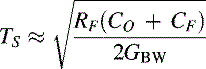 where
where
(8.6)
CO = the DAC internal capacitance.
RF = the feedback resistor.
CF = the compensation capacitance.
GBW = the small signal unity gain bandwidth product of the output amplifier.
18.7. Increasing Op Amp Buffer Amplifier Current and Voltage
Process limitations of op amps limit the power that can be dissipated at the output. Unfortunately, some applications require the DAC to interface to loads that dissipate considerable power. These include actuators, position solenoids, stepper motors, loudspeakers, vibration tables, positioning tables—the possibilities are endless.
While several “power op amps” are available that can drive heavy loads, they usually compromise several other specifications to achieve the high power operation. Input voltage offset, input current, and input capacitance can be decades higher than the designer is accustomed to and make these power op amps unsuitable for direct interface with a DAC as a replacement for the buffer op amp.
The power booster stage can be designed discretely or a prepackaged amplifier of some sort, depending on what is needed for the application. Sometimes, high current is required for driving loads such as actuators and stepper motors. Audio applications can require a lot of wattage to drive loudspeakers. This implies a higher voltage rail than op amps commonly operate at. This and other high voltage applications can operate off of and generate lethal voltages. The designer needs to be extremely careful not to create an unsafe product or be electrocuted while developing it.
The power stage is most often included in the feedback loop of the op amp circuit, so that the closed loop can compensate for power stage errors. This is not always possible if the voltage swing of the output exceeds that of the op amp voltage rails. In these cases, a voltage divided version of the output should be used.
The three broad categories of booster are current boosters, voltage boosters, and boosters that do both. All of them work on the same principle: Anything put inside the feedback loop of the op amp is compensated for—the output voltage swings to whatever voltage it needs to make the voltage at the buffer op amp inputs equal.
18.7.1. Current Boosters
Current boosters usually use some variation of the class-B push/pull amplifier topology (Figure 18.16).
 |
| Figure 18.16 DAC output current booster. |
The circuit in Figure 18.16 has been employed for decades—many resources are available to design exact component values. It boosts current because the output impedance of the op amp has been bypassed and used as the driver for the base of the npn and pnp power transistors. The two diodes compensate for the VBE drop in the transistors, whose bases are biased by two resistors off of the supplies. The output of the booster stage is fed back to the feedback resistor in the DAC to complete the feedback loop. The output impedance of the stage is limited by only the characteristics of the output transistors and small emitter resistors. Modern power transistors have such high frequency response that this circuit may oscillate. The RC snubber network and a small inductor in series with the load can be used to damp the oscillation—or be omitted if oscillation is not a problem. Beware of varying transistor betas, however.
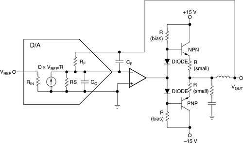
18.7.2. Voltage Boosters
If even more current is needed or the output voltage swing must be more than ±15 V, the booster stage can be operated at voltages higher than the buffer amplifier potentials. A designer might be tempted to try the circuit of Figure 18.17.
 |
| Figure 18.17 Incorrect method of increasing voltage swing of DACs. |
Any time there are higher voltage rails on the output section, there are potential hazards. This circuit illustrates a common misapplication:
• The whole reason for using the booster amp is to allow the VOUT to swing to a ±100 V rail. If this circuit is operated in the unity gain mode (external RF = 0), the VOUT swings only ±15 V maximum. There is no need for the ±100 V rail. That voltage rail is there to allow voltage gain.
• If the circuit is operated with a gain (external R larger than 0), the external RF adds to the internal RF to create the gain: 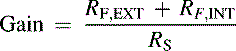
(18.7)
The problem with this is that the wattage of the resistors increases as the external voltage rail increases. The designer has control over the wattage of the external RF but no control whatsoever over internal RF or RS. Because these resistors are fabricated on the IC, their wattage is limited. Even if the wattage rating of the internal resistors is meticulously observed, they may have undesirable thermal coefficients if allowed to dissipate that wattage. Resistor self-heating changes the resistance according to its rated temperature coefficient (maximum). The external resistor is sure to have a different thermal coefficient from the internal resistors, causing a gain error. The designer may never have encountered the effects of resistor self-heating before, because through hole and surface mount devices have enough bulk to minimize the effect of self-heating. At the geometries present on IC DACs, resistor self-heating is a much more pronounced effect. It produces a nonlinearity error in the DAC output.
This effect is most pronounced in high resolution converters, where the geometry is the smallest. The designer, therefore, must limit the current in the feedback resistor if at all possible. Figure 18.18 shows a method of achieving gain control while keeping the high current path out of the internal feedback resistor.
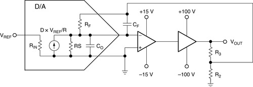 |
| Figure 18.18 Correct method of increasing voltage range. |
In Figure 18.18,
• R3 and R2 are selected to ensure that the feedback voltage to the DAC internal RF can never exceed the DAC rated limits.
• R3 and R2, of course, have to be the correct power rating. R2, in particular, has to be carefully selected. If it burns out, the feedback loop presents hazardous voltages to the DAC. R3, which drops the bulk of the voltage, has to dissipate considerable wattage.
If the combination of voltage swing and power ratings cannot be balanced to achieve a working design, the only choice left to the designer is to break the feedback loop and live with the loss of accuracy. For AC applications, this may be acceptable.
18.7.3. Power Boosters
The preceding two types of boosters can, of course, be combined to produce more power. In audio applications, for example, a ±15 V power supply limits the output power to 112.5 W, absolute maximum, into an 8 Ω load. To increase the power, the voltage rails must also be increased, with all of the cautions of the previous subsection observed.
18.7.4. Single Supply Operation and DC Offsets
A DAC power circuit is not the right place to try to apply single supply design techniques. In audio applications, a single supply design forces a large coupling capacitor, which distorts and limits low frequency response. In DC applications, a DC offset continually drives the load, which has to dissipate the excess voltage through its internal resistance as heat.
Nevertheless, some applications may require a DC offset. The designer is fortunate in that a precision reference is already available in the circuit. The reference drives the resistor network in the DAC and may be external or internal to it. In most cases, an internal reference is brought out to a pin on the device. It is important for the designer not to load the reference excessively, as that directly affects DAC accuracy (Figure 18.19).
 |
| Figure 18.19 Single supply DAC operation. |
In the circuit in Figure 18.19, the output of the buffer amplifier is shifted up in DC level by 1/2 VREF (not 1/2 VCC). VREF is selected because it is much more stable and accurate than VCC. The four resistors in the level shifter circuit must be highly accurate and matched, or this circuit will contribute to gain and offset errors. Thermal errors, however, cannot be compensated for, because the external resistors are probably going to have a different thermal drift than those on the IC. This technique is limited to applications that will see only a small change in ambient temperature.
..................Content has been hidden....................
You can't read the all page of ebook, please click here login for view all page.