4
Optical Properties
Hiroyuki Fujiwara1, Yukinori Nishigaki1, Akio Matsushita2 and Taisuke Matsui2
1Gifu University, Department of Electrical, Electronic and Computer Engineering, 1‐1 Yanagido, Gifu, 501‐1193, Japan
2Panasonic Corporation, Technology Innovation Division, 3‐1‐1 Yagumo‐naka‐machi, Moriguchi City, Osaka, 570‐8501, Japan
4.1 Introduction
Strong light absorption within absorbers is one of the critical conditions for the efficient operation of solar cells. For hybrid perovskite absorbers that are formed typically by a spin coating process, the formation of a thicker layer (>1 μm) is difficult and a high absorption coefficient (α) is particularly important. Fortunately, various hybrid perovskites exhibit high α in the visible/ultraviolet (UV) region as shown in Figure 4.1, which summarizes the α spectra of methylammonium lead iodide (CH3NH3PbI3; MAPbI3) [1], formamidinium lead iodide (HC(NH2)2PbI3; FAPbI3) [2], MAPbBr3 [3], CsFAPb(I1−xBrx)3 [4], and FAMA(Sn,Pb)I3 (see also tabulated data in Appendix A). In particular, hybrid perovskites indicate α of ∼104 cm−1 in the band gap (Eg) region, which is comparable to representative solar cell materials including GaAs, CuInGaSe2, and Cu2ZnSnS4 (see Figure 1.5).

Figure 4.1 α spectra of various hybrid perovskites, determined by spectroscopic ellipsometry for MAPbI3 [1], FAPbI3 [2], MAPbBr3 [3], CsFAPb(I1−xBrx)3 and FAMA(Sn,Pb)I3. For CsFAPb(I1−xBrx)3, the optical constants reported in Ref. [4] were adjusted slightly by extra roughness correction [5]. In the figure, three spectra of CsFAPb(I1−xBrx)3 with x of 0.0, 0.2, and 0.4 are shown. The numerical optical‐constant values in the figure are summarized in Appendix A.
Hybrid perovskites show unique light absorption properties in a wide energy region extending from 10−6 to 6 eV, due to the interband transition in the visible/UV region, chemical bond absorption in the infrared (IR) region, optical phonon absorption in the terahertz (THz) region, and organic cation orientation in a GHz range (Section 4.2). Remarkably, because hybrid perovskites consist of an organic cation and inorganic scaffold, these materials exhibit the optical signature characteristics of both organic and inorganic parts.
To date, numerous results have been reported for the optical properties of hybrid perovskites in the visible/UV region [1–53]. The Eg of hybrid perovskites changes largely by the choice of the A‐, B‐, and X‐site species in ABX3 perovskites (Section 4.3). Furthermore, for hybrid perovskites, a wide variety of alloys can be formed, allowing for a large variation of Eg by the mixture of different cations and anions (Section 4.3). For the absolute α values of the perovskite materials, however, controversial results have been reported [1][8–17]. The reason for the inconsistent optical data is an important and complex issue (Section 4.4). Nevertheless, it is now established that careful measurement and analysis based on spectroscopic ellipsometry (SE) provides accurate α values [1, 5]. In Figure 4.1, the reliable α spectra determined by SE have been summarized.
In APbX3 perovskites, when the A‐site cation species is varied, the magnitude of α in the Eg region changes and the variation of the X‐site halide anion shifts the entire spectrum in the energy direction (Section 4.5). On the other hand, hybrid perovskites exhibit a sharp absorption tail (Section 4.6), which is a significant advantage of hybrid perovskite absorbers. For temperature variation, unlike other conventional semiconductor materials, the perovskite compounds show a slight Eg increase with temperature (Section 4.7).
As evidenced from Figure 4.1, APbI3 hybrid perovskites show negligible excitonic band‐edge absorption, whereas MAPbBr3 exhibits an absorption peak due to exciton formation. The absence of an exciton peak in APbI3 confirms the efficient generation of electron–hole carriers, and numerous studies have consistently demonstrated the weak exciton character of MAPbI3 perovskites (Section 4.8).
This chapter describes the fundamental and unique optical characteristics of hybrid perovskite materials in detail. We emphasize that, in interpreting device characteristics and performing device simulations, accurate optical spectra are of critical importance.
4.2 Light Absorption in MAPbI3
The interaction of light with materials can be described completely by two important physical quantities: refractive index n and extinction coefficient k [54]. The n is related to the wavelength λ of light (or electromagnetic wave), and λ of light reduces to λ/n in a material with n. In contrast, k is related to the magnitude of an electromagnetic wave and light intensity reduces strongly in a material with high k. The above (n, k) can be considered as a single complex number (complex refractive index) defined by
From k, a well‐known α is obtained:
From Maxwell's equations, N is defined by a complex dielectric constant (ε = ε1 − iε2) [54]:
Thus, from Eqs. (4.1) and (4.3), we obtain
Although the representation is slightly different, all k, α, and ε2 show the light absorption characteristics. In particular, k = α = ε2 = 0 when the light absorption is zero and we further obtain ε1 = n2 from Eq. 4.4 in this condition.
Figure 4.2 shows the dielectric function (ε = ε1 − iε2) of MAPbI3, obtained experimentally in a quite wide energy region extending from 10−6 to 6 eV. In this figure, ε1 is shown by a linear scale, whereas the ε2 values are indicated by a logarithmic scale. The MAPbI3 hybrid perovskite shows unique light absorption characteristics (i.e. ε2 > 0) in different energy regions, which can be categorized into four distinct regions: (i) semiconductor‐type light absorption in the visible/UV region, (ii) chemical bonding absorption in the IR region, (iii) optical phonon absorption in the THz region, and (iv) orientational absorption induced by the organic cation rotation in the GHz region. The experimental spectra of each corresponding region, shown in Figure 4.2, are taken from Ref. [1] (visible/UV), Ref. [55] (IR), Ref. [56] (THz), and Ref. [57] (GHz).

Figure 4.2 Dielectric function (ε = ε1 − iε2) of MAPbI3 obtained experimentally in a quite wide energy region extending from 10−6 to 6 eV. The ε2 spectrum shows the light absorption characteristics. In the figure, the experimental spectra reported for the visible/UV [1], IR [55], GHz [56], and THz [57] regions were summarized, whereas the dotted line indicates the unreported region. All the spectra were obtained at room temperature, except for the dielectric function in the GHz region, which was measured at 210 K. The ε1 is shown by a linear scale, while ε2 is indicated by a logarithmic scale. The εs and ε∞ represent the static dielectric constant and high‐frequency dielectric constant, respectively.
Source: Shirayama et al. [1]; Glaser et al. [55]; Sendner et al. [56]; Anusca et al. [57].
Physically, all the light absorption in Figure 4.2 can be explained by considering the dipole formation. An electromagnetic wave is essentially the wave of an electric field E, and when the light enters a material, the electric field separates the charge existing within the material, creating the positive‐charge‐rich and negative‐charge‐rich regions (i.e. electric dipole). In the visible/UV region, a nonzero dipole matrix element for the optical transition from the valence to conduction bands (i.e. interband transition) leads to the light absorption and the onset of ε2 > 0 essentially corresponds to Eg of MAPbI3 (Section 4.2.1). The dipole formation by the vibration of the atoms in the IR region generates sharp absorption features, yet with a weak ε2 amplitude of ∼0.5 (Section 4.2.2).
One distinctive feature of MAPbI3 light absorption is an extraordinary strong optical phonon absorption with a considerably large amplitude of ε2 ∼ 50 (Section 4.2.3). Another unique feature, which is absent in conventional semiconductors, is a very strong light absorption by orientational dipole formation. The MA+ cation has a permanent dipole of C(δ−)–N(δ+), where δ+ and δ− represent the positive and negative partial charges, respectively. Accordingly, when light enters (i.e. when the electric field is applied), MA+ rotates so that the orientation of the C–N dipole is aligned along the oscillation direction of the electric field. This slow collective motion of MA+, which occurs in the GHz range, leads to rather strong light absorption with an ε2 peak amplitude of 27. A similar orientational absorption occurs for H2O molecules with a dipole of H(δ+)–O(δ−) [58]. In microwave ovens, the microwave absorption of the H2O molecules in the GHz range is utilized as the heating system. A large ε2 absorption by MA+ orientation is consistent with the fact that MA+ is preferentially aligned under the presence of the electric field.
The ε1 spectrum of MAPbI3 in Figure 4.2 has a complex structure. As known well, the ε1 and ε2 spectra are not independent and the ε1 spectrum is calculated from the ε2 spectrum by applying Kramers–Kronig relations (see Appendix A). The ε1 optical response is generally characterized by two physical values: namely, the static dielectric constant (εs) and high‐frequency dielectric constant (ε∞). These values are obtained from the flat ε1 regions observed between the IR and visible/UV region (ε∞) and between the GHz and THz region (εs). The absolute ε1 value essentially shows the total amount of electric dipoles created by the electric field and, as the frequency of the alternating electric field increases, ε1 gradually decreases. For example, we observe ε1 = 83.6 at E = 10−6 eV. This includes all the dipole‐formation effects of the MA+ orientational, phonon, IR, and interband absorption. However, the motion of MA+ orientation is essentially slow, and the MA+ orientational dipoles disappear when the polarity of the electric field switches too fast at a higher frequency of light. At E = 10−3 eV, therefore, by the elimination of the orientational dipole, ε1 decreases to εs = 34.9. At higher E (i.e. higher frequency), the disappearance of the phonon absorption further reduces ε1 to ε∞ = 5.0 and ε1 finally becomes one (i.e. ε1 = n = 1) at a quite high frequency. At very low frequency (<104 Hz), on the other hand, ε1 is reported to increase to ∼100 due to the ion migration [16, 51].
Figure 4.3 summarizes (a) ε∞ and (b) εs of MAPbX3 (X = I−, Br−, and Cl−), which are compared with those reported for tetrahedral‐bonding crystals [59]. For ε∞, all the hybrid perovskites show notably small values. Note that ε∞ = ε1 = n2 because k = 0 in the ε∞ region. If compared with the values of GaAs (ε∞ = 10.9, n = 3.30), the corresponding values of MAPbI3 (ε∞ = 5.0, n = 2.23) are remarkably low. The small ε∞ (or n∞) of the hybrid perovskites can be interpreted by the large optical void created by the presence of the organic cations, as the polarizability of organic cations is negligible in the visible region. In other words, the optical density of hybrid perovskites is intrinsically low.
Figure 4.3 (a) High‐frequency dielectric constantε∞ and (b) static dielectric constantεs vs. Eg of MAPbX3 (X = I−, Br−, and Cl−) and tetrahedral‐bonding crystals. The ε∞ value of MAPbI3 from Figure 4.2 was used, whereas those of MAPbBr3 and MAPbCl3 were extracted from the dielectric function model parameters in Ref. [7] assuming E = 0 eV. The εs values of MAPbX3[56] were determined by the THz measurements (Section 4.2.3). For tetrahedral‐bonding semiconductors, the values of Ref. [59] were adopted.
In contrast, εs of hybrid perovskites determined by Sendner et al. [56] is surprisingly high, compared with other conventional compound semiconductors. The high εs in hybrid perovskites is consistent with quite strong optical phonon absorption in the materials. This extraordinary strong optical photon absorption is a unique feature of hybrid perovskites and is proposed to lower carrier mobility by enhanced phonon scattering (Section 6.3.4).
In the following sections, further details regarding the light absorption in the visible/UV region (Section 4.2.1), in the IR region (Section 4.2.2), and in the THz region (Section 4.2.3) are described.
4.2.1 Visible/UV Region
Figure 4.4 shows the dielectric function (ε = ε1 − iε2), (n, k) spectra, and α spectrum of MAPbI3 in the visible/UV region [1]. The determination of accurate optical data for hybrid perovskites has been challenging because of the (i) extensive roughness, which corresponds to λ of the probe light (∼500 nm) [10, 60] and (ii) quite fast degradation that occurs by humid air [61]. To avoid these serious problems, the optical spectra of Figure 4.4 were obtained from an ultra‐smooth MAPbI3 layer with a roughness of 5 nm and its measurement was performed in a N2‐globe bag without exposing the sample to air at all [1].
Figure 4.4 Dielectric function (ε = ε1 − iε2), (n, k) spectra, and α spectrum of MAPbI3 in the visible/UV region, determined by spectroscopic ellipsometry characterization [1]. These spectra are consistent with those of Figures 4.1 and 4.2. In the figure, the dielectric function expressed by the Tauc–Lorentz model is shown (see Appendix A). The gray lines indicate the contribution of each Tauc–Lorentz peak. The peak parameter values and the numerical optical‐constant values of MAPbI3 are summarized in Appendix A.
Source: Modified from Shirayama et al. [1].
In Figure 4.4, it can be seen that the spectra shapes of ε1 and ε2 resemble those of n and k, respectively, and the α spectrum is calculated from k by Eq. 4.2. The onsets of ε2, k, and α spectra essentially correspond to the Eg of MAPbI3 (1.61 eV). In the high energy region of MAPbI3, there exist clear absorption peaks at 2.53, 3.24, and 5.65 eV, which are labeled as the E1, E2, and E3 optical transitions, respectively. Note that a small peak at ∼4.5 eV is caused by the presence of PbI2 at the surface and interface. This PbI2 peak becomes stronger with the perovskite degradation that occurs near the surface region [61]. The thin lines for (ε1, ε2) represent the results of the parameterization using the Tauc–Lorentz model (Appendix A). In this scheme, the ε2 spectrum is expressed as the sum of all the Tauc–Lorentz peaks (see Appendix A for more details).
To understand the light absorption phenomena in hybrid perovskites, quite extensive density functional theory (DFT) analyses have been performed [1–3, 17, 38, 42]. Nevertheless, the DFT calculation results vary significantly depending on the calculation (or approximation) method (Section 5.4). It has been found, however, that DFT optical spectra calculated based on a rather simple approximation (generalized gradient approximation within the Perdew–Burke–Ernzerhof, i.e. PBE scheme) demonstrate remarkable agreement with the experimental spectra (Figure 5.8), enabling us to perform detailed optical transition analyses.
Figure 4.5 summarizes the result of the optical transition analysis performed for MAPbI3 by DFT (PBE): (a) band structure and (b) charge density profiles near the conduction band minimum (CBM) and valence band maximum (VBM) [1]. Importantly, the light absorption of MAPbI3 in the visible/UV region can be expressed by semiconductor‐type optical transitions (i.e. the electron transition from the valence band to the conduction band). Moreover, the E0, E1, and E2 transition peaks observed experimentally in Figure 4.4 are consistent with the direct optical transitions at high symmetry points at R, M, and X points in the Brillouin zone, respectively (see arrows in Figure 4.5). For the E2 peak, however, there are three transition components labeled as E2,a–c. The above assignment of the optical transitions was determined by calculating the ε2 spectral contributions for each pair of the valence and conduction bands [1, 5].

Figure 4.5 Optical transitions in MAPbI3: (a) band structure and (b) charge density profiles near CBM (1.4–1.6 eV) and VBM (−0.2 to 0 eV) of MAPbI3, calculated within PBE. The inset of (a) shows the high symmetry points in the Brillouin zone of the assumed pseudo‐cubic structure (Figure 5.4a). The arrows in (a) indicate the direct semiconductor‐type optical transitions, corresponding to the E0–E2 transitions in Figure 4.4.
Source: Shirayama et al. [1].
The band structure of Figure 4.5 clearly shows the direct‐transition‐type band structure; the VBM and CBM are positioned at the same symmetry point of R. When the spin–orbit coupling (SOC) effect is considered in the DFT calculations, however, the conduction band splits into two bands (Rashba splitting) and the band structure becomes slightly indirect (see Figure 5.8). Nevertheless, the DFT optical spectra calculated by incorporating the Rashba splitting effect disagree with the experimental spectra; in particular, (i) the light absorption strength is seriously underestimated and (ii) the absorption tail broadens excessively when the Rashba splitting is considered (Figures 5.8 and 5.9). Because the DFT results change significantly depending on the approximation method, the DFT results must be justified according to the experimental results, particularly for hybrid perovskites that include the dynamic motion of organic cations. Consequently, the direct‐gap formation in MAPbI3 is quite appropriate to interpret the experimental results correctly (see Section 5.4.2 for further details).
As shown in Figure 4.5b, the CBM of MAPbI3 consists of Pb 6p orbital, whereas the VBM is composed of Pb 6s and I 5p states (Figure 5.11a). Since the CBM and VBM of MAPbI3 are anti‐bonding states (Figure 5.12), the charge profiles of Pb 6s, Pb 6p, and I 5p are separated and localized near the Pb and I atoms. The light absorption in semiconductors can be understood simply from the overlap of the electronic charge in the valence and conduction states [62]. In MAPbI3, the Pb 6s charge in the VBM overlaps with the Pb 6p charge in the CBM and thus the light absorption at the VBM → CBM occurs by Pb 6s → 6p transition [62]. In the energy region slightly above CBM, the dispersive I charge is present [1] and its contribution becomes important. Importantly, there are no electronic charges (or states) of MA+ near CBM and VBM (Figure 5.11a); thus, the direct light absorption by MA+ is negligible in the visible/UV region. In other words, the visible/UV light absorption in hybrid perovskites occurs only in the inorganic framework (i.e. PbI3− scaffold in APbI3).
4.2.2 IR Region
In hybrid perovskites, weak light absorption occurs in the IR region due to the dipole moments created by the vibration of the organic cations. Figure 4.6 shows the ε2 spectrum of MAPbI3 obtained in the IR region [55]. In MAPbI3, the main IR peaks originate from ![]() vibrational modes:
vibrational modes: ![]() bending (∼1550 cm−1) and stretching (∼3150 cm−1) modes. As discussed by Glaser et al. [55], the peak position of the N–H stretching mode is sensitive to hydrogen bonding and the shift of the N–H stretching peak toward lower energy indicates the formation of the strong hydrogen bonding in MAPbI3 (see also Figure 3.15).
bending (∼1550 cm−1) and stretching (∼3150 cm−1) modes. As discussed by Glaser et al. [55], the peak position of the N–H stretching mode is sensitive to hydrogen bonding and the shift of the N–H stretching peak toward lower energy indicates the formation of the strong hydrogen bonding in MAPbI3 (see also Figure 3.15).
Figure 4.6 ε2 spectrum of MAPbI3 in the IR region determined from transmission measurements. The result of the peak assignment analysis based on theoretical calculations (second‐order Møller–Plesset perturbation theory) is also indicated. There exist symmetric (s) and asymmetric (a) modes for stretching and bending vibrations.
Source: Glaser et al. [55].
The ε2 peaks in the IR region have a Lorentz shape, and the dielectric function can be expressed as a sum of a Lorentz model peak:
where Aj, ω0,j, and γj represent the amplitude, peak frequency, and broadening parameters of the jth peak, respectively. The peak positions (i.e. ω0,j) obtained from the above analysis are summarized in Table 4.1. All the IR peak positions are essentially independent of the X‐site halide anion, although the IR peak shifts slightly toward a higher wavenumber in the order of I → Br → Cl [55].
Table 4.1 IR peak positions for major vibrational modes in MAPbI3, reported by Glaser et al. [55].
| Peak position (cm−1) | Vibrational mode |
|---|---|
| 911 | CH3– |
| 960 | C–N stretching |
| 1250 | CH3– |
| 1469 | |
| 1577 | |
| 3132 | |
| 3179 |
The result of the peak assignment is also shown.
Source: Modified from Glaser et al. [55].
4.2.3 THz Region
One of the important features of hybrid perovskite optical properties is the quite strong optical phonon absorption by the inorganic framework. Figure 4.7 shows the ε2 and Im(−1/ε) spectra of MAPbI3 [56] and GaAs [59]. The ε2 peaks show transverse optical (TO) phonon modes, where Im(−1/ε) is called the loss function, representing the longitudinal optical (LO) phonon modes. The TO and LO phonon peaks can be described by the Lorentz line shape shown in Eq. 4.6. Based on a DFT study, the strong TO peak at ωTO = 63 cm−1 has been assigned to a Pb–I stretching‐like vibration, whereas the peak of ωTO = 32 cm−1 is due to a Pb–I–Pb rocking‐like vibration [56]. The peak positions of the two LO phonon modes are 40 and 133 cm−1. The slight change in the phonon frequencies has been observed in MAPbBr3 and MAPbCl3 by the effect of ionic masses [56].
![Schematic illustration of ε2 and Im(-1/ε) spectra of [56] and GaAs [59] at room temperature, which show the transverse optical (TO) phonon and longitudinal optical (LO) phonon modes, respectively.](https://imgdetail.ebookreading.net/2023/10/9783527347292/9783527347292__9783527347292__files__images__c04f007.png)
Figure 4.7 ε2 and Im(−1/ε) spectra of MAPbI3[56] and GaAs [59] at room temperature, which show the transverse optical (TO) phonon and longitudinal optical (LO) phonon modes, respectively. The ε2 amplitude of GaAs is reduced to a third of the original, and Im(−1/ε) amplitude of GaAs is also reduced to half for clarity.
In Figure 4.7, the TO and LO absorption peaks of MAPbI3 are significantly broader, compared with GaAs. In fact, the peak half width of ωLO = 133 cm−1 (25 cm−1) is 10 times greater than that of the GaAs LO peak (2.4 cm−1). The extraordinary phonon peak broadening observed in MAPbI3 has been attributed to the dynamic disorder of PbI6 octrahedra [56]. In other words, the “soft and flexible” inorganic cage (see Table 6.1) allows unusually strong phonon absorption. The enhanced phonon absorption in MAPbI3 can be evidenced from the considerably larger integrated peak area in MAPbI3, compared with GaAs.
The very large εs of MAPbI3, shown in Figures 4.2 and 4.3, can also be understood from the phonon absorption spectra. In general, εs is estimated by a simple theory known as the Lyddane–Sachs–Teller relation [59]:

In non‐polar materials (Si, for example), ωLO = ωTO; thus, we obtain εs = ε∞ from Eq. 4.7. In MAPbI3, the peak separation between ωTO and ωLO is considerably greater than that in GaAs, leading to a remarkably large εs, which has been estimated to be εs = 33.5 from Eq. 4.7 [56].
Important points in MAPbI3 phonon absorption include the (i) low energy peak position of ωLO and (ii) strong LO‐phonon absorption that leads to εs ≫ ε∞. Carriers in semiconductors interact with LO phonons (phonon coupling), and the small ωLO and εs ≫ ε∞ observed in MAPbI3 are indicative of the carriers being scattered by LO‐phonon vibration (see Eq. (6.6)). In fact, it has been proposed that the low mobility of ∼100 cm2/(V s) observed in MAPbI3 (see Figure 6.4) originates from the strong LO phonon scattering, although different interpretations exist (Section 6.3.4).
4.3 Band Gap of Hybrid Perovskites
The Eg of a light absorber is one of the most critical physical parameters directly influencing the solar cell conversion efficiency, as only limited Eg (Eg = 1.0–1.6 eV) is allowed for efficient devices ( Figure 12.1). Nevertheless, the reported Eg values of hybrid perovskites are rather controversial [1, 10, 12][18–46]. The origin of such controversy can be attributed to the different analysis methods and contributions of inaccurate α spectra from which the Eg values are extracted. In this section, we review the Eg analysis of MAPbI3 (Section 4.3.1) and see the Eg values of different hybrid perovskites (Section 4.3.2) and perovskite alloys (Section 4.3.3).
4.3.1 Band Gap Analysis of MAPbI3
Table 4.2 summarizes various Eg values of MAPbI3 reported using different measurement and analysis techniques [1, 10, 12][18–27]. The reported Eg depends strongly on the measurement technique, independent of the sample forms (i.e. thin film or single crystal). In high‐precision ellipsometry characterization, consistent values of 1.60–1.61 eV have been obtained [1, 8, 10, 12, 18]. The transmission (T) measurements result in slightly reduced Eg values (1.57–1.61 eV) [20–23]. Note that Eg can be underestimated seriously, particularly when the baseline of the α spectrum is elevated by roughness scattering (Section 4.4.2). In the reflectance (R) measurements, α spectrum is deduced using a relation known as the Kubelka–Munk function: α ∝ F(R) = (1 − R)2/(2R). The Eg values obtained from this scheme are, however, low (1.50–1.52 eV) [25–27].
Table 4.2 Various Eg values of MAPbI3, reported using different measurement and analysis techniques.
| Measurement | Analysis | Sample | Eg (eV) | References |
|---|---|---|---|---|
| Ellipsometry | Critical point | Thin film | 1.61 | [1] |
| Ellipsometry | Critical point | Thin film | 1.61 | [18] |
| TA3) | — | Thin film | 1.61 | [19] |
| Transmission | Tauc plot | Thin film | 1.61 | [20] |
| Ellipsometry | DF Modelingb) | Single crystal | 1.60 | [12] |
| Ellipsometry | DF Modeling | Thin film | 1.60 | [10] |
| Transmission | Tauc plot | Thin film | 1.60 | [21] |
| Transmission | Linear fitting | Thin film | 1.57 | [22] |
| Transmission | NDc) | Thin film | 1.57 | [23] |
| EQE | Linear fitting | Thin filmd) | 1.55 | [24] |
| Reflection | Kubelka–Munk | Single crystal | 1.52 | [25] |
| Reflection | Kubelka–Munk | Single crystal | 1.51 | [26] |
| Reflection | Kubelka–Munk | Thin film | 1.50 | [27] |
The results are shown in order of decreasing Eg.
aTransient absorption spectroscopy.
bEg is determined from modeling (parameterization) of dielectric function (DF).
cNot described.
dReported as the Eg of MAPbI2Cl.
The Eg of MAPbI3 is often represented by 1.55 eV based on the work of Lee et al. [24]. This Eg is deduced as the onset of the external quantum efficiency (EQE) spectrum at λ ∼ 800 nm. However, the Eg obtained from this indirect approach reflects the absorption onset, which shifts toward a reduced energy by tail absorption. The EQE spectrum varies by external effects including film thickness, light scattering, and back‐side reflection, and accurate Eg determination is rather difficult from EQE measurements.
In general, the most reliable Eg analysis is performed by critical point analysis, where Eg is extracted from the theoretical fitting of the second derivative (ε1, ε2) spectra [54, 63]:

where A, φ, Ep, and Γ are the amplitude, phase, position, and width of the peak, respectively. Depending on the band structure, the critical point is classified into one dimension (j = −1/2), two dimensions (j = 0), three dimensions (j = 1/2), or excitonic (j = −1).
Figure 4.8 shows the results of the MAPbI3 critical point analysis performed for the experimental dielectric function of Figure 4.4 [1]. In the second derivative spectra, the spectral feature in only the transition peak (critical point) region is extracted, enabling the reliable determination of the transition energy. From the fitting analysis based on Eq. 4.8, Eg has been determined to be 1.61 ± 0.01 eV. The exact same Eg was reported in another critical point analysis [18]. The transition absorption (TA) spectroscopy also shows the negative TA peak at 1.61 eV due to photobleaching observed for a direct‐gap semiconductor [19]. Thus, the appropriate Eg of MAPbI3 is 1.61 eV.
Figure 4.8 Result of the critical point analysis performed for the experimental dielectric function of MAPbI3 shown in Figure 4.4. A similar good fitting is also obtained for d2ε2/dE2. From the analysis, Eg of MAPbI3 is determined to be 1.61 ± 0.01 eV.
Source: Shirayama et al. [1].
4.3.2 Band Gap of Basic Perovskites
The Eg values of various hybrid perovskites reported in Refs. [1, 2, 4, 18, 20][32–36] are summarized in Table 4.3. Due to the variation of the measurement and analysis methods, inconsistent Eg values have been reported, particularly for Sn‐based materials including FASnI3 [32, 34, 37], MASnI3 [20, 34][38–42], and CsSnI3 [33, 34][43–46]. Moreover, strong excitonic peaks are present in the absorption spectra of APbBr3 and APbCl3. In these cases, Eg can no longer be determined from the onset of the absorption; rather it must be deduced by separating the contribution of the excitonic peak from the band‐to‐band (interband) absorption. Such analyses have been performed for MAPbBr3 [35] and MAPbCl3 [36] in Table 4.3. Note that, if conventional Eg analyses are performed for excitonic absorption spectra, Eg is seriously underestimated.
Table 4.3 Eg of various perovskites.
| Material | Measurement | Analysis | Eg (eV) | References |
|---|---|---|---|---|
| FASnI3 | Ellipsometry | Critical point | 1.40 | [32] |
| MASnI3 | Transmission | Tauc plot | 1.28 | [20] |
| CsSnI3 | Transmission | Steepest gradient | 1.36 | [33] |
| FAPbI3 | Ellipsometry | Critical point | 1.55 | [2, 18] |
| Cs0.17FA0.83PbI3 | Ellipsometry | Tauc plot | 1.55 | [4] |
| MAPbI3 | Ellipsometry | Critical point | 1.61 | [1] |
| CsPbI3 | Transmission | Steepest gradient | 1.76 | [33] |
| CsSnBr3 | Transmission | ND | 1.81 | [34] |
| MASnBr3 | Transmission | ND | 2.13 | [34] |
| FAPbBr3 | Ellipsometry | Critical point | 2.30 | [18] |
| MAPbBr3 | Ellipsometry | Elliott's formula | 2.39 | [35] |
| CsPbBr3 | Transmission | ND | 2.31 | [34] |
| FASnBr3 | Transmission | ND | 2.63 | [34] |
| CsSnCl3 | Transmission | ND | 2.88 | [34] |
| CsPbCl3 | Transmission | ND | 2.99 | [34] |
| FAPbCl3 | Transmission | ND | 3.02 | [34] |
| MAPbCl3 | Transmission | Exciton model | 3.16 | [36] |
| MASnCl3 | Transmission | ND | 3.50 | [34] |
| FASnCl3 | Transmission | ND | 3.55 | [34] |
The Eg of the perovskite materials is shown in order of increasing Eg. The absolute Eg is influenced by the measurement and analysis methods (see Table 4.2); the Eg values derived from transmission measurements could be underestimated slightly, compared with ellipsometry results.
a Eg was determined after performing extra roughness correction [5] for the optical spectrum reported in Ref. [4].
b Not described.
Figure 4.9 shows the variation of Eg with the (a) A‐site cation and (b) X‐site anion in hybrid perovskites. In APbI3 materials, Eg increases slightly in the order of FA → MA → Cs. A systematic DFT study reveals that this Eg variation with the A‐site cation is caused by the change in the Pb–I–Pb bond angle; the larger A‐site cation (Table 3.3) leads to a Pb–I–Pb angle nearer to 180°, which in turn reduces the Eg (Figure 5.14). This phenomenon has been interpreted by the anti‐bonding character of the Pb and I orbitals (see Section 5.5.1).
Figure 4.9 Variation of Eg with (a) the A‐site cation and (b) the X‐site anion in various hybrid perovskites. In (a), Eg variations in APbI3 and ASnI3 with the A‐site cation are shown, whereas the Eg variations in MAPbX3, FAPbX3, and MASnX3 with the X‐site anion are summarized in (b). The Eg values are adopted from those presented in Table 4.3.
In contrast, there is no clear trend for Eg when the A‐site cation is changed in ASnI3. However, unlike MASnI3, which exhibits the pseudo‐cubic structure, FASnI3 and CsSnI3 have orthorhombic structures (see Table 3.2) and their Eg values cannot be compared directly. The DFT study of CsSnI3, for example, shows that the crystal structure changes Eg significantly [64]. Moreover, due to the small ionic radius of Sn2+, the Sn–I–Sn bond angle in MASnI3 is almost 180° [33]. In ASnI3 perovskites, therefore, the Eg variation by the lattice expansion is considered more important [65].
It can be observed from Figure 4.9b that the influence of the X‐site anion is considerably greater than those of the A‐site and B‐site cations; the variation of the halide anion from I− to Br− increases Eg drastically by ∼0.8 eV. The increase in Eg by the order of I → Br → Cl follows the general trend that a lighter atom leads to Eg widening.
4.3.3 Band Gap Variation in Perovskite Alloys
To control Eg in a wide range, the alloying by I–Br and Pb–Sn mixing has been performed for hybrid perovskites. Figure 4.10a shows the Eg variations with the Br content x in Cs0.17FA0.83Pb(I1−xBrx)3 and Cs0.05FA0.8MA0.15Pb(I1−xBrx)3. The Eg values have been extracted from the optical data in Appendix A using the Tauc analysis. Up to x = 0.4, the Eg of the perovskites increases linearly with x:
![Schematic illustration of variations of Eg in (a) CsFAPb(I1-xBrx)3 and CsFAMAPb(I1-xBrx)3 with x, (b) protect MAPb(I1-xBrx)3 with x, (c) MA(Pb1-xSnx)I3 with x, and (d) band edge positions of /MAPbBr3 and /MASnI3 relative to the vacuum level in eV. The result of CsFAPb(I1-xBrx)3 in (a) was obtained after performing the extra roughness correction [5] protect for protect the optical data of Ref. [4].](https://imgdetail.ebookreading.net/2023/10/9783527347292/9783527347292__9783527347292__files__images__c04f010.png)
Figure 4.10 Variations of Eg in (a) CsFAPb(I1−xBrx)3 and CsFAMAPb(I1−xBrx)3 with x, (b) MAPb(I1−xBrx)3 with x, (c) MA(Pb1−xSnx)I3 with x, and (d) band edge positions of MAPbI3/MAPbBr3 and MAPbI3/MASnI3 relative to the vacuum level in eV. The result of CsFAPb(I1−xBrx)3 in (a) was obtained after performing the extra roughness correction [5] for the optical data of Ref. [4].
Figure 4.10b shows the Eg variation of MAPb(I1−xBrx)3 in a wider x range (x = 0–1), which indicates a similar Eg increase, yet with a slight Eg bowing [22]:
For the Eg determination, a simple analysis has been employed (see Eg = 1.57 eV of Ref. [22] in Table 4.2). For FAPb(I1−xBrx)3 and CsPb(I1−xBrx)3, similar Eg variations have been confirmed (see Figure 18.7). In the case of MAPb(Br1−xClx)3, a slight Eg bowing expressed by Eg = 2.415 + 0.53x + 0.30x2 has also been reported [36].
Interestingly, for the Sn–Pb mixed alloys (i.e. A(Sn,Pb)I3), a significant Eg bowing has been confirmed. Figure 4.10c summarizes the Eg change for the Sn content x in MA(Pb1−xSnx)I3 for which Eg is expressed by the following equation [42]:
where ![]() and
and ![]() show the Eg values of MAPbI3 (1.6 eV) and MASnI3 (1.3 eV), respectively. Notably, Eg bowing has also been confirmed when different A‐site cations are adopted in A(Pb,Sn)I3 (see Figures 10.8 and 18.12).
show the Eg values of MAPbI3 (1.6 eV) and MASnI3 (1.3 eV), respectively. Notably, Eg bowing has also been confirmed when different A‐site cations are adopted in A(Pb,Sn)I3 (see Figures 10.8 and 18.12).
The origin of the monotonous Eg increases in APb(I,Br)3, and the strong Eg bowing in A(Sn,Pb)I3 can be explained by the energy alignment of the VBM and CBM [42] (Figure 4.10d). When the X‐site anion is changed in MAPbX3, for example, the energy position of the CBM moves upward, whereas that of the VBM shifts downward by I → Br exchange. When Br is incorporated into APbI3, therefore, the Eg widening occurs by the energy shift of VBM and CBM. In contrast, the band alignment between MAPbI3 and MASnI3 is staggered (type‐II alignment) and the Sn alloying with Pb leads to a smaller gap material, whose optical transition occurs from the Sn‐derived VBM state to the Pb‐based CBM state. This Eg reduction is helpful for an all‐perovskite tandem application, as the Eg reduction in the Sn‐based alloy increases the photosensitivity in the long λ region (see Chapter 18).
4.4 True Absorption Coefficient of MAPbI3
Light absorption in the visible/UV region is of critical importance in operating solar cells. Although extensive studies have been made to determine the α spectra of hybrid perovskites in the visible/UV region, the absolute α values obtained using spectroscopic ellipsometry and transmission/reflectance (T/R) measurements are seriously controversial [1][8–17]. In this section, we review the basic principles of optical measurements (Section 4.4.1) and discuss how we can obtain accurate optical constants (Section 4.4.2).
4.4.1 Principles of Optical Measurements
Figure 4.11 shows the principles of (a) ellipsometry and (b) T/R optical measurements. Ellipsometry is a high‐precision optical characterization technique, in which the optical constants are determined by the change in polarized light upon reflection [54]. This technique employs p‐ and s‐polarized light waves, whose oscillation directions of the electric field are parallel and perpendicular to the incident plane, respectively (see Figure 4.11a). Depending on the (n, k) values, the polarized light undergoes different changes upon light reflection and ellipsometry measures two angles (ψ, Δ), which express the relative amplitude and phase difference between the p‐ and s‐polarized waves, respectively. The ψ is essentially related to the n component, whereas the phase variation Δ is generated by the light absorption (i.e. k). In ellipsometry, therefore, two defining values of optical constants can be determined from a single measurement.
Figure 4.11 Principles of (a) ellipsometry and (b) transmission/reflectance (T/R) measurements. Ellipsometry measures two angles (ψ, Δ), which express the relative amplitude and phase difference between the p‐ and s‐polarized light (electromagnetic) waves. In (b), the white arrows show non‐ideal surface light scattering and the light reflection at the thin‐film/substrate interface, which enhance the nominal absorptance (A) if simple analyses are performed.
Although ellipsometry allows the determination of highly accurate values, its data analysis tends to be complicated. In particular, the exact optical modeling of an entire sample structure as well as all the (n, k) values of the constituent layers is necessary [54]. Moreover, ellipsometry spectra (particularly Δ spectrum) are extremely sensitive to surface/interface structures; improper modeling of these structures generates strong artifacts and, often, the adjustment of roughness thickness on a few‐Å scale is required [5].
In T/R measurements, on the other hand, the absolute light intensities (i.e. square of the electric field; I ∝ |E|2) of a thin‐film/substrate structure are generally characterized. In this case, the phase information obtained in ellipsometry is lost and, therefore, α is obtained analytically. The simplest approach often adopted to determine α is the application of Beer's law: I(d) = I0 exp(−αd), where I0 and I(d) show the light intensity on the surface (d = 0) and at the film thickness of d, respectively. In this case, α is obtained from the measured absorbance (Ab) based on a simple relation:
Thus, from a known d, α can be determined using Ab. In another approach, the following relation has been adopted [14]:
where A is the absorptance that can be estimated from A = 1 − R − T (i.e. T + R + A = 1). Eq. 4.13 is particularly useful to eliminate the effect of interference.
In the above simple T/R approaches, however, the estimation of the accurate α of hybrid perovskites is difficult because the (i) light scattering that occurs on a film surface and (ii) optical interference caused by the light reflection at a thin‐film/substrate interface are completely neglected. In particular, hybrid perovskite layers formed by one‐step spin coating generally exhibit very large roughness with a size comparable to the wavelength of incident light (λ ∼ 500 nm) [10, 60]. Accordingly, the strong light scattering occurs in these layers, which in turn enhances the nominal α due to the increased light pass length. Note that, in Eqs. (4.12) and (4.13), the αd component is considered and, when the analytical film thickness d is fixed, the enhanced absorption by light scattering is misinterpreted as high α in the film. The optical interference effect, caused by the finite light reflection on the surface and at the interface, also enhances the effective optical pass length within the layer and, similarly, nominal α increases if a simple layer thickness d is adopted in the analysis.
As a result, the α values derived particularly from simple T/R analyses are generally overestimated. The T/R measurements themselves are straightforward and are useful for obtaining the overall shape of the α spectra and rough α values; however, the extra care is necessary to interpret the absolute α value. On the other hand, ellipsometry measurements are far less sensitive to light scattering as only the specular reflection component is measured [6, 7]. In ellipsometry analysis, the optical interference effect is also modeled explicitly. Nevertheless, rigorous optical modeling of the layer structures is necessary for accurate optical‐constant determination by ellipsometry.
4.4.2 Interpretation of α Variation
Figure 4.12a shows the α spectra of MAPbI3 determined by spectroscopic ellipsometry [1][8–12] and T/R‐based techniques [13–16]. The reported MAPbI3 α spectra are quite different, although the spectral shape is rather similar. The highly controversial α results do not originate from measurement techniques; all the ellipsometry and T/R results are essentially inconsistent. In particular, some results show very high α values even below the Eg of MAPbI3.

Figure 4.12 (a) α spectra of MAPbI3 determined by spectroscopic ellipsometry [1][8–12] and T/R‐based techniques [13–16] and (b) α simulation result obtained when a hypothetical roughness thickness (dr) is assumed for Shirayama's result. The dotted line indicates the Eg position of 1.61 eV. In (b), the α spectrum of dr = 0 nm corresponds to the α spectrum of Shirayama et al. and the nominal α (pseudo‐absorption coefficient, 〈α〉) increases largely with increasing dr, which is modeled by the Bruggeman effective medium theory with a 50 vol% of void in the roughness layer.
Source: Shirayama et al. [1].
The large α variation observed for the ellipsometry results can be explained by the extensive roughness in MAPbI3 layers. Specifically, the α spectrum of Shirayama et al. which is shown in Figure 4.4, was obtained from an ultra‐smooth MAPbI3 layer where the effect of the roughness is minimized. Notice that the α values of Shirayama et al. show the smallest values among the results. Figure 4.12b shows the α simulation result obtained when a hypothetical roughness thickness (dr) is assumed for the Shirayama's result [1]. In the figure, the α spectrum of dr = 0 nm corresponds to the spectrum reported by Shirayama et al. and the nominal α (pseudo‐absorption coefficient, 〈α〉) increases largely with increasing dr. As explained previously in Figure 4.11a, Δ in ellipsometry can be related to the light absorption. However, the roughness also induces the large phase lag and, in simplified ellipsometry analyses, the Δ change generated by the roughness is misinterpreted as the α increases [5]. As confirmed from Figure 4.12, the ellipsometry results of Refs. [8, 9] are well reproduced by the roughness simulation. In fact, when the roughness correction is performed for the α spectra of Refs. [8, 9], the recalculated α spectra show excellent agreement with Shirayama's result [5]. In some ellipsometry studies, on the other hand, (T, R) spectra are analyzed simultaneously, in addition to (ψ, Δ) ellipsometry spectra [10, 66, 67]. However, when extensive sample roughness modifies the T/R spectra, the validity of such (ψ, Δ, R, T) analyses must be examined carefully.
It is highly likely that the large α confirmed for the T/R results is caused by strong light scattering due to large roughness. In fact, some α spectra obtained from the T/R analyses show large non‐zero α values in the region below Eg, which can be understood by the light scattering effect of the roughness. Note that any transmission loss generated by roughness light scattering can be misinterpreted as light absorption in the simple analysis described above. In a well‐cited α spectrum reported by De Wolf et al. [14], the α was determined from Eq. 4.11; therefore, the influence of the light scattering and optical interference was not included in this analysis, and the large analysis error is expected. It is often argued that MAPbI3 shows the highest α among solar cell materials based on the result of De Wolf et al. However, when accurate α spectrum is compared, the α of MAPbI3 is comparable to those of GaAs and CdTe (see Figure 1.5). In the past, CuInSe2 (CISe) had been considered to have the highest α (∼105 cm−1) among all the solar cell materials [68]. Nevertheless, this was also artifact caused by the roughness scattering in the T/R measurements [5], and actual α of CISe is comparable to other solar cell materials [69].
To justify the α result of Shirayama et al., complementary analyses were performed. Figure 4.13 shows the experimental α spectrum of Shirayama et al., and additional analysis results were obtained from spectroscopic ellipsometry (SE), EQE, and DFT analyses. In SE, a multi‐sample analysis was performed [1] and the calculated (ψ, Δ) spectra (solid lines) show almost perfect agreement with the experimental spectra (open circles).

Figure 4.13 Experimental α spectrum of MAPbI3 reported by Shirayama et al. [1]. The α spectrum is consistent with other analysis results obtained for spectroscopic ellipsometry (SE) [1], external quantum efficiency (EQE) [1], and DFT [70] analyses. In the SE analysis, a MAPbI3 layer with different thickness (85 nm) is analyzed. In the EQE analysis, a semi‐transparent MAPbI3 solar cell with a structure of MgF2/glass/SnO2:F/TiO2/MAPbI3/spiro‐OMeTAD/MoOx/ZnO:Al/MgF2[71] is analyzed by adopting the α spectrum in the figure (see Section 11.4). The calculated Jsc (16.5 mA/cm2) shows excellent agreement with the experimental value (16.7 mA/cm2). The DFT calculation is performed by PBE using a very high mesh density of 16 × 16 × 16 k mesh [70] (see Section 5.2).
In the EQE analysis, a semi‐transparent MAPbI3 solar cell reported in Ref. [71] was analyzed using the α spectrum of Shirayama et al. In this solar cell, a rear metal electrode is not present and the light absorption properties can be studied with greater accuracy due to the lack of metal back‐side reflection. As shown in the figure, the calculated EQE spectrum (solid line) shows excellent agreement with the measured spectrum (open circles) and the short‐circuit current density (Jsc) obtained from the analysis agrees quite well with the experimental value [1]. It should be emphasized that, when an α spectrum with greater absolute values is applied for the EQE simulation, Jsc is seriously overestimated [1].
In Figure 4.13, the experimental α spectrum of Shirayama et al. is further compared with the DFT α spectrum [70]. For the DFT calculation, the PBE functional was employed (see Section 5.2). The magnitude of α determined theoretically by DFT shows excellent overall agreement with the experimental spectrum; therefore, the experimental light absorption is consistent with the dipole transition expected from rigorous theoretical calculation.
As discussed above, there are inherent difficulties for obtaining reliable optical spectra of hybrid perovskites and the extracted experimental optical spectrum must be justified based on other complementary methods including optical device simulations and DFT calculations. The key points for accurate optical‐constant characterization are the (i) preparation of smoother perovskite layers to reduce the roughness effect, (ii) optical measurements without exposing the samples to air to avoid rapid surface degradation, and (iii) application of a high‐precision ellipsometry technique with exact optical modeling.
4.5 Universal Rules for Hybrid Perovskite Optical Properties
The optical properties of hybrid perovskite materials vary with the choice of A‐site cations and X‐site anions. The A‐site cation has a notable effect on absolute α values (Section 4.5.1), while the X‐site anion shifts the α spectrum in the energy direction (Section 4.5.2). In this section, we discuss the universal rules for the optical property variation with the A‐site cation and X‐site anion species.
4.5.1 Variation with Center Cation
Figure 4.14 summarizes the α spectra obtained with the variation of the A‐site cations. All the α spectra were determined by high‐precision ellipsometry characterization. These results show that the α in the band‐edge region changes with the choice of organic cation; FAPbI3 shows a low α, whereas the α in MAPbI3 increases. The incorporation of a small amount of Cs (17 at.%) into FAPbI3 increases the band‐edge α. High α is also maintained in a CsFAMAPb(I,Br)3 triple‐cation perovskite even though the Cs and MA contents in the material are relatively low.

Figure 4.14 α spectra obtained with the variation of the A‐site cations. Theα spectra of MAPbI3[1], FAPbI3[2], Cs0.17FA0.83PbI3, and Cs0.05FA0.8MA0.15Pb(I0.95Br0.05)3 are shown. The α spectra are consistent with those shown in Figure 4.1. For CsFAPbI3, the optical constants reported in Ref. [4] were adjusted slightly by extra roughness correction [5].
The unexpected large influence of the A‐site cation on α has been discussed based on DFT calculations [2]. As mentioned above, in the visible/UV region, there is no direct light absorption by the organic cations and the optical transition is characterized by Pb(6s) + I(5p) → Pb(6p). Nevertheless, the distribution of the I‐5p charge densities varies largely depending on the cation species due to the hydrogen bonding interaction (I⋯HN). Interestingly, when the hydrogen bonding is formed, the I‐5p charge disappears due to the reduction of the N–I distance. This electrostatic interaction (the anti‐coupling effect [2]) can be adopted to explain the α variation in Figure 4.14. In particular, the α in the perovskite increases in the order of FA → MA → Cs due to the weakening hydrogen bonding interaction (see Figure 10.11). Nevertheless, what is less apparent is the high α observed for the FA‐based mixed‐cation perovskites. The molecular dynamics simulations of CsFAPbI3 show that rather strong distortion occurs for the FAPbI3 cubic structure by incorporation of Cs+ [72]. Thus, a large‐scale DFT calculation is necessary to further verify the effect of the mixed A‐site cations on α.
4.5.2 Variation with Halide Anion
Figure 4.15 summarizes the variations of hybrid perovskite α spectra with the X‐site anion, determined by spectroscopic ellipsometry characterization. All the optical constant data of the figure are summarized in Appendix A. In MAPbX3, the entire spectrum shifts toward higher energy as the X‐site halide anion becomes lighter [3]. In the case of MAPbBr3 and MAPbCl3, the presence of the excitonic absorption increases the α in the Eg region. For the APb(I1−xBrx)3 alloys in Figure 4.15, the entire α spectrum slides toward higher energy without an amplitude change. A similar trend can be confirmed for the A(Sn,Pb)I3 material shown in Figure 4.1. This simple horizontal α‐shift can be explained by applying the sum rule [73]:

The sum rule requires that, when the ε2 spectrum is shifted toward a higher energy by ΔE, the ε2 amplitude is reduced by a factor of f = E/(E + ΔE) [2, 74].
![Schematic illustration of variations of hybrid perovskite α spectra with the X-site anion, determined by spectroscopic ellipsometry characterization. In the figure, the reported! extit{$alpha$} spectra α spectra of [1], MAPbBr3 [3], and MAPbCl3 [3] are shown. For CsFAPb(I,Br)3, the optical constants reported in Ref. [4] were adjusted slightly by extra roughness correction [5]. All the optical constant data in this figure are summarized in Appendix A.](https://imgdetail.ebookreading.net/2023/10/9783527347292/9783527347292__9783527347292__files__images__c04f015.png)
Figure 4.15 Variations of hybrid perovskite α spectra with the X‐site anion, determined by spectroscopic ellipsometry characterization. In the figure, the reported α spectra of MAPbI3 [1], MAPbBr3 [3], and MAPbCl3 [3] are shown. For CsFAPb(I,Br)3, the optical constants reported in Ref. [4] were adjusted slightly by extra roughness correction [5]. All the optical constant data in this figure are summarized in Appendix A.
Figure 4.16a shows an example of the ε2 shift calculation based on the sum rule. In this figure, the ε2 spectrum of MAPbI3 is shifted toward higher energy while reducing the ε2 amplitude using f. From the shifted ε2 spectra, the corresponding ε1 spectra are calculated by applying the Kramers–Kronig integration [54, 73]:

where P shows the principal value of the integral. From a set of (ε1, ε2) obtained from the above calculation, α(E) can further be deduced. Figure 4.16b shows the α spectra calculated from the above approach. It can be seen that the resulting α spectrum shifts horizontally in the energy direction without the amplitude change. The above scheme can be applied to calculate the optical constants of an alloy with an arbitrary composition (or ΔE) and is particularly helpful in designing a perovskite top cell in a tandem architecture.
![Schematic illustration of spectral shift calculation of !spectral shift calculation of based on the sum rule: variation of (a) ε2 and (b) α spectra. In the figure, the ε2 spectrum of [1] is shifted toward higher energy by δE = 0.3 and 0.6 eV. The horizontal shift of the α spectrum by alloying of the X-site anions can be reproduced by this model.](https://imgdetail.ebookreading.net/2023/10/9783527347292/9783527347292__9783527347292__files__images__c04f016.png)
Figure 4.16 Spectral shift calculation of MAPbI3 based on the sum rule: variation of (a) ε2 and (b) α spectra. In the figure, the ε2 spectrum of MAPbI3 [1] is shifted toward higher energy by ΔE = 0.3 and 0.6 eV. The horizontal shift of the α spectrum by alloying of the X‐site anions can be reproduced by this model.
When the dielectric function is modeled by the Tauc–Lorentz model (see Figure 4.4), the alloy dielectric function can be modeled by simply increasing the corresponding peak energy positions toward higher energy. From the Tauc–Lorentz model parameters described in Appendix A, the optical constants of various perovskite alloys can be calculated. Such an approach has previously been adopted in the EQE simulation program (e‐ARC software) [75], explained in Figure 11.13.
4.6 Subgap Absorption Characteristics
The sharp absorption feature at the Eg edge (subgap region) is critical for solar cell absorbers as strong tail absorption increases the saturation current density (J0), leading to significant open‐circuit voltage (Voc) reduction [76]. The tail absorption in semiconductors can be analyzed quantitatively by the Urbach energy (EU), obtained by considering an exponential tail state [77]:
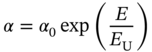
where α0 shows a proportional constant. Thus, EU can be estimated easily from the relation of lnα ∝ E/EU.
Figure 4.17 shows the (a) result of the Urbach analysis performed for MAPbI3 and (b) variation of EU with Eg of various hybrid perovskites in Figures 4.1 and 4.15. MAPbI3 exhibits a sharp band‐edge characterized by a low EU of 15 meV [14, 70]. Photothermal deflection spectroscopy (PDS) further shows that the sharp absorption tail is maintained over a wide α range (α = 10–104 cm−1) [14]. A low EU is also observed for the mixed‐cation perovskite alloys (Figure 4.17b), confirming that the A‐site cation and X‐site anion mixing does not lead to band‐edge fluctuation. A similar low EU has also been observed in Sn‐based materials (see Figure 10.7). Note that, in APbBr3 and APbCl3, the EU analysis becomes difficult as the band‐edge excitonic absorption prevents the tail state analysis.
![Schematic illustration of (a) Urbach analysis performed for !Urbach analysis [70] and (b) variation of EU with Eg obtained for various hybrid perovskites shown in Figures 4.1 and 4.15. The line in (a) indicates the result of linear fitting based on lnα ∝ E/EU.](https://imgdetail.ebookreading.net/2023/10/9783527347292/9783527347292__9783527347292__files__images__c04f017.png)
Figure 4.17 (a) Urbach analysis performed for MAPbI3[70] and (b) variation of EU with Eg obtained for various hybrid perovskites shown in Figures 4.1 and 4.15. The line in (a) indicates the result of linear fitting based on lnα ∝ E/EU.
Source: Based on Nishiwaki et al. [70].
A sharp absorption edge observed in hybrid perovskites is supported by the theoretical calculations. Figure 4.18a compares the experimental and DFT α spectra of MAPbI3 in the band‐edge region [70]. Both spectra overlap almost perfectly even though a perfect crystal structure at 0 K is assumed in the DFT calculation. This result indicates that the formation of an unintentional tail state is almost completely suppressed in the experimental perovskite crystal. A DFT study further shows that small EU in MAPbI3 is an inherent character. Figure 4.18b shows the relation of the experimental EU and DFT absorption edge energy (EDFT) derived from ln(αDFT) ∝ E/EDFT [70]. This result shows that the EU and EDFT of MAPbI3 are notably smaller, compared with the other solar cell materials in the figure. The small EDFT of MAPbI3 has been attributed to the sharp density‐of‐states (DOS) distribution in the band edge region (see Figure 5.11b). In the case of Cu2ZnSnSe4 (CZTSe) and Cu2ZnSnS4 (CZTS), EU is considerably greater than EDFT due to intense cation mixing in the experimental crystals [70], severely limiting Voc of these solar cells [76].

Figure 4.18 (a) Experimental and DFT α spectra of MAPbI3 in the band‐edge region and (b) relation of the experimental EU and DFT absorption edge energy (EDFT).
Source: Nishiwaki et al. [70].
It should be emphasized that the above DFT results were obtained for the direct‐gap band structure shown in Figure 4.5 (i.e. within PBE). When the SOC interaction is considered, EDFT increases significantly to 37 meV due to the conduction band splitting (i.e. Rashba splitting) and the calculated EDFT deviates from the experimental EU (see Figure 5.9). Accordingly, Rashba splitting is inconsistent with the sharp absorption edge confirmed experimentally.
4.7 Temperature Effect on Absorption Properties
Almost all semiconductors show Eg reduction with a temperature increase [77]. Nevertheless, unlike conventional semiconductors, hybrid perovskites show Eg widening with temperature (T) [28–31]. In this section, we discuss the unique Eg variation of MAPbI3 with T.
Figure 4.19a shows the ε2 spectral variation with T in MAPbI3 [29]. The ε2 absorption feature changes dramatically by the γ (orthorhombic) → β (tetragonal) phase change that occurs at T ∼ 160 K (see also Figure 3.13). In the low‐T γ phase, a clear excitonic peak is present, whereas the interband absorption dominates at higher temperatures. In both regions, the band‐edge absorption shifts toward higher energy with increasing T, although Eg shows a rapid reduction by the γ → β phase change. A similar spectral variation can be confirmed in Figure 4.19b, where α values in the band‐edge region are shown for different T [30]. In the figure, a high‐energy spectral shift with increasing T and a sudden drop of Eg at T ∼ 160 K can be confirmed more clearly. The black and red regions observed at low T are consistent with the excitonic peak.
![Schematic illustration of (a) ε2 spectral variation of extit{ε}$_{2}$ !spectral variation of with temperature T, (b) change in band-edge α with T, (c) variation of the Eg position with T. In (a), non-zero ε2 values observed below Eg are most likely due to the contribution of the roughness. In (c), the results of three studies [28-30] are summarized but each result was shifted slightly so that Eg at room temperature shows a consistent value of 1.61 eV.](https://imgdetail.ebookreading.net/2023/10/9783527347292/9783527347292__9783527347292__files__images__c04f019.png)
Figure 4.19 (a) ε2 spectral variation of MAPbI3 with temperature T, (b) change in band‐edge α with T, (c) variation of the Eg position with T. In (a), non‐zero ε2 values observed below Eg are most likely due to the contribution of the roughness. In (c), the results of three studies [28–30] are summarized but each result was shifted slightly so that Eg at room temperature shows a consistent value of 1.61 eV.
Source: (a) Jiang et al. [29]. (b) Davies et al. [30]. Licensed under CC BY 4.0. (c) Foley et al. [28]; Jiang et al. [29]; Davies et al. [30].
Figure 4.19c shows the variation of the Eg position with T. In this figure, three results [28–30] are summarized to cover a wider T range and each result is shifted slightly such that the Eg at room temperature shows a consistent value of 1.61 eV. The large Eg reduction by 0.1 eV at 160 K can be attributed to the change in the Pb–I–Pb bond angle by the γ → β transition [30]. Similar to the effect of the A‐site cation in APbI3 (Figure 4.9a), Eg decreases when the Pb–I–Pb bond angle becomes collinear. Since the Pb–I–Pb angle of the β phase is nearer 180° (see Figure 3.15), the Eg decreases by the sharp phase transition at T ∼ 160 K. On the other hand, the β → α transition at 327 K does not influence Eg, as the crystal structures are essentially similar.
The increase of Eg with T, observed in two different regimes in MAPbI3, can be fitted by a linear model of
The observed increase in Eg with T has been attributed to the lattice expansion and enhanced electron–phonon coupling [31]. The Eg widening at high T has also been confirmed in other hybrid perovskites including FAPbI3, FAPbBr3, and MAPbBr3 [53].
4.8 Excitonic Properties of Hybrid Perovskites
To explain the efficient carrier generation in hybrid perovskites, the excitonic character of MAPbI3 has been investigated and discussed extensively [16, 30, 35][47–52]. The exciton is a hydrogen‐like structure generated for a hole in the valence band and an electron in a conduction band, which are attracted to each other through the Coulomb force. In general, the exciton formation in materials is characterized from the exciton binding energy (EX) derived for an electron–hole Coulomb attraction and the stability of the exciton can be gauged simply from the magnitude of EX. Table 4.4 summarizes EX values and their analysis methods reported for MAPbX3 [16, 30, 35][47–50]. One simple way to determine EX is to apply the Wannier equation:

where m0, q, and ε0 indicate the electron mass, electron charge, and vacuum permittivity, respectively [16]. The two important variables in Eq. 4.19 are the exciton effective mass μ and dielectric constant ε (i.e. ε = ε1). By assuming μ = 0.6–0.7 m0 and ε = 70 determined experimentally, a very low EX of ∼2 meV has been derived for MAPbI3 [16]. Since the thermal energy at room temperature (i.e. kBT = 26 meV) is considerably greater than EX, the exciton formation is negligible in MAPbI3. Consistent low EX values in the range 2–8 meV have also been reported for MAPbI3 (see Table 4.4), although the discussion of the appropriate EX values continues [51, 52]. On the other hand, in the DFT calculation within PBE, excitonic interaction (i.e. electron–hole Coulomb attraction) is neglected completely. Thus, the excellent agreement observed between the experimental and DFT spectra in Figure 4.13 confirms that the excitonic character is negligible in MAPbI3.
Table 4.4 Exciton binding energy (EX) in hybrid perovskites at room temperature.
| Material | Method | EX (meV) | References |
|---|---|---|---|
| MAPbI3 | Impedance analysis | ∼2 | [16] |
| Magneto‐optical characterization | ∼2 | [47] | |
| Absorption analysis | 6 | [48] | |
| Absorption (Elliott's theory) | ∼8 | [30] | |
| Absorption (Elliott's theory) | 25 | [49] | |
| MAPbBr3 | Absorption (Elliott's theory) | 41.6 | [35] |
| Absorption (Elliott's theory) | 64 | [49] | |
| Absorption (f‐sum rule) | 60 | [50] | |
| MAPbCl3 | Absorption (Elliott's theory) | 69 | [49] |
Analysis methods for each report are also indicated.
In MAPbBr3 and MAPbCl3, EX values become larger than the room‐temperature thermal energy. Thus, for these perovskites, the exciton is stable at room temperature, generating the clear excitonic feature in the absorption spectra (Figure 4.15).
References
- 1 Shirayama, M., Kadowaki, H., Miyadera, T. et al. (2016). Phys. Rev. Appl. 5: 014012.
- 2 Kato, M., Fujiseki, T., Miyadera, T. et al. (2017). J. Appl. Phys. 121: 115501.
- 3 Leguy, A.M.A., Azarhoosh, P., Alonso, M.I. et al. (2016). Nanoscale 8: 6317.
- 4 Tejada, A., Braunger, S., Korte, L. et al. (2018). J. Appl. Phys. 123: 175302.
- 5 Fujiwara, H., Fujimoto, S., Tamakoshi, M. et al. (2017). Appl. Surf. Sci. 421: 276.
- 6 Fujiwara, H. and Collins, R.W. (2018). Spectroscopic Ellipsometry for Photovoltaics: Fundamental Principles and Solar Cell Characterization, vol. 1. Cham: Springer Nature.
- 7 Fujiwara, H. and Collins, R.W. (2018). Spectroscopic Ellipsometry for Photovoltaics: Applications and Optical Data of Solar Cell Materials, vol. 2. Cham: Springer Nature.
- 8 Ball, J.M., Stranks, S.D., Hörantner, M.T. et al. (2015). Energy Environ. Sci. 8: 602.
- 9 Xing, G., Mathews, N., Lim, S.S. et al. (2014). Nat. Mater. 13: 476.
- 10 Löper, P., Stuckelberger, M., Niesen, B. et al. (2015). J. Phys. Chem. Lett. 6: 66.
- 11 Jiang, Y., Green, M.A., Sheng, R., and Ho‐Baillie, A. (2015). Sol. Energy Mater. Sol. Cells 137: 253.
- 12 Leguy, A.M.A., Hu, Y., Campoy‐Quiles, M. et al. (2015). Chem. Mater. 27: 3397.
- 13 Sun, S., Salim, T., Mathews, N. et al. (2014). Energy Environ. Sci. 7: 399.
- 14 De Wolf, S., Holovsky, J., Moon, S.‐J. et al. (2014). J. Phys. Chem. Lett. 5: 1035.
- 15 Xing, G., Mathews, N., Sun, S. et al. (2013). Science 342: 344.
- 16 Lin, Q., Armin, A., Nagiri, R.C.R. et al. (2015). Nat. Photonics 9: 106.
- 17 Fujiwara, H., Kato, M., Tamakoshi, M. et al. (2018). Phys. Status Solidi A 215: 1700730.
- 18 Ndione, P.F., Li, Z., and Zhu, K. (2016). J. Mater. Chem. C 4: 7775.
- 19 Yamada, Y., Nakamura, T., Endo, M. et al. (2014). Appl. Phys. Express 7: 032302.
- 20 Zhao, B., Abdi‐jalebi, M., Tabachnyk, M. et al. (2017). Adv. Mater. 29: 1604744.
- 21 Colella, S., Mosconi, E., Fedeli, P. et al. (2013). Chem. Mater. 25: 4613.
- 22 Noh, J.H., Im, S.H., Heo, J.H. et al. (2013). Nano Lett. 13: 1764.
- 23 Eperon, G.E., Stranks, S.D., Menelaou, C. et al. (2014). Energy Environ. Sci. 7: 982.
- 24 Lee, M.M., Teuscher, J., Miyasaka, T. et al. (2012). Science 338: 643.
- 25 Stoumpos, C.C., Malliakas, C.D., and Kanatzidis, M.G. (2013). Inorg. Chem. 52: 9019.
- 26 Baikie, T., Fang, Y., Kadro, J.M. et al. (2013). J. Mater. Chem. A 1: 5628.
- 27 Kim, H.‐S., Lee, C.‐R., Im, J.‐H. et al. (2012). Sci. Rep. 2: 591.
- 28 Foley, B.J., Marlowe, D.L., Sun, K. et al. (2015). Appl. Phys. Lett. 106: 243904.
- 29 Jiang, Y., Soufiani, A.M., Gentle, A. et al. (2016). Appl. Phys. Lett. 108: 061905.
- 30 Davies, C.L., Filip, M.R., Patel, J.B. et al. (2018). Nat. Commun. 9: 293.
- 31 Saidi, W.A., Poncé, S., and Monserrat, B. (2016). J. Phys. Chem. Lett. 7: 5247.
- 32 Ghimire, K., Zhao, D., Yan, Y., and Podraza, N.J. (2017). AIP Adv. 7: 075108.
- 33 Rajagopal, A., Stoddard, R.J., Hillhouse, H.W., and Jen, A.K.‐Y. (2019). J. Mater. Chem. A 7: 16285.
- 34 Tao, S., Schmidt, I., Brocks, G. et al. (2019). Nat. Commun. 10: 2560.
- 35 Yang, Y., Yan, Y., Yang, M. et al. (2015). Nat. Commun. 6: 7961.
- 36 Kumawat, N.K., Dey, A., Kumar, A. et al. (2015). ACS Appl. Mater. Interfaces 7: 13119.
- 37 Koh, T.M., Krishnamoorthy, T., Yantara, N. et al. (2015). J. Mater. Chem. A 3: 14996.
- 38 Umari, P., Mosconi, E., and De Angelis, F. (2015). Sci. Rep. 4: 4467.
- 39 Hao, F., Stoumpos, C.C., Chang, R.P.H., and Kanatzidis, M.G. (2014). J. Am. Chem. Soc. 136: 8094.
- 40 Im, J., Stoumpos, C.C., Jin, H. et al. (2015). J. Phys. Chem. Lett. 6: 3503.
- 41 Anaya, M., Correa‐Baena, J.P., Lozano, G. et al. (2016). J. Mater. Chem. A 4: 11214.
- 42 Goyal, A., McKechnie, S., Pashov, D. et al. (2018). Chem. Mater. 30: 3920.
- 43 Shum, K., Chen, Z., Qureshi, J. et al. (2010). Appl. Phys. Lett. 96: 221903.
- 44 Yu, C., Chen, Z., Wang, J.J. et al. (2011). J. Appl. Phys. 110: 063526.
- 45 Chen, Z., Yu, C., Shum, K. et al. (2012). J. Lumin. 132: 345.
- 46 Sabba, D., Mulmudi, H.K., Prabhakar, R.R. et al. (2015). J. Phys. Chem. C 119: 1763.
- 47 Miyata, A., Mitioglu, A., Plochocka, P. et al. (2015). Nat. Phys. 11: 582.
- 48 Yamada, Y., Nakamura, T., Endo, M. et al. (2015). IEEE J. Photovoltaics 5: 401.
- 49 Saba, M., Quochi, F., Mura, A., and Bongiovanni, G. (2016). Acc. Chem. Res. 49: 166.
- 50 Sestu, N., Cadelano, M., Sarritzu, V. et al. (2015). J. Phys. Chem. Lett. 6: 4566.
- 51 Herz, L.M. (2018). J. Phys. Chem. Lett. 9: 6853.
- 52 Jiang, Y., Wang, X., and Pan, A. (2019). Adv. Mater. 31: 1806671.
- 53 Wright, A.D., Verdi, C., Milot, R.L. et al. (2016). Nat. Commun. 7: 11755.
- 54 Fujiwara, H. (2007). Spectroscopic Ellipsometry: Principles and Applications. West Sussex: Wiley.
- 55 Glaser, T., Müller, C., Sendner, M. et al. (2015). J. Phys. Chem. Lett. 6: 2913.
- 56 Sendner, M., Nayak, P.K., Egger, D.A. et al. (2016). Mater. Horiz. 3: 613.
- 57 Anusca, I., Balčiūnas, S., Gemeiner, P. et al. (2017). Adv. Energy Mater. 7: 1700600.
- 58 Miyata, K. and Zhu, X.‐Y. (2018). Nat. Mater. 17: 379.
- 59 Adachi, S. (1999). Optical Properties of Crystalline and Amorphous Semiconductors: Materials and Fundamental Principles. Norwell: Kluwer Academic Publishers.
- 60 Jung, H.S. and Park, N.‐G. (2015). Small 11: 10.
- 61 Shirayama, M., Kato, M., Miyadera, T. et al. (2016). J. Appl. Phys. 119: 115501.
- 62 Kato, M., Nishiwaki, M., and Fujiwara, H. (2020). Phys. Rev. Mater. 4: 035402.
- 63 Lautenschlager, P., Garriga, M., Vina, L., and Cardona, M. (1987). Phys. Rev. B 36: 4821.
- 64 Huang, L.Y. and Lambrecht, W.R.L. (2013). Phys. Rev. B 88: 165203.
- 65 Prasanna, R., Gold‐Parker, A., Leijtens, T. et al. (2017). J. Am. Chem. Soc. 139: 11117.
- 66 Guerra, J.A., Tejada, A., Korte, L. et al. (2017). J. Appl. Phys. 121: 173104.
- 67 Manzoor, S., Häusele, J., Bush, K.A. et al. (2018). Opt. Express 26: 27441.
- 68 Jaffe, J.E. and Zunger, A. (1984). Phys. Rev. B 29: 1882.
- 69 Minoura, S., Maekawa, T., Kodera, K. et al. (2015). J. Appl. Phys. 117: 195703.
- 70 Nishiwaki, M., Nagaya, K., Kato, M. et al. (2018). Phys Rev. Mater. 2: 085404.
- 71 Kranz, L., Abate, A., Feurer, T. et al. (2015). J. Phys. Chem. Lett. 6: 2676.
- 72 Ghosh, D., Smith, A.R., Walker, A.B., and Islam, M.S. (2018). Chem. Mater. 30: 5194.
- 73 Marder, M.P. (2010). Condensed Matter Physics. Hoboken, NJ: Wiley.
- 74 Nishiwaki, M. and Fujiwara, H. (2020). Comput. Mater. Sci. 172: 109315.
- 75 Nakane, A., Tampo, H., Tamakoshi, M. et al. (2016). J. Appl. Phys. 120: 064505.
- 76 Kato, Y., Fujimoto, S., Kozawa, M., and Fujiwara, H. (2019). Phys Rev. Appl. 12: 024039.
- 77 Pankove, J.I. (1971). Optical Processes in Semiconductors. New York: Dover.