
Chapter 5
Buck-Based LED Drivers
Abstract
This chapter describes switching buck (step-down) regulators. These include synchronous and asynchronous switching, also hysteretic, peak current, and average current control schemes. Design examples are given for a common type of controller. Dimming techniques are described, including triac dimming. A double-buck circuit is also described.
Keywords
dimming
buck
double buck
triac
synchronous
asynchronous
The first switching LED driver that we will study is the buck converter, which is the simplest of the switching drivers. The buck converter is also known as a step-down converter and is used in applications where the load voltage is less than the supply voltage. In a buck converter circuit, shown in Fig. 5.1, inductor L and an LED are wired in series, with the LED connected to common.

Figure 5.1 Basic Buck LED Driver.
Switch SW1 is used to connect the supply voltage to the inductor, which causes the current to flow through both inductor and LED, so the LED emits light. The inductor limits the rate at which the current increases and stores energy during this time. A control circuit will force SW1 to open when the current through the LED reaches a set limit. At this time the inductor has energy stored, which must now be released (an alternative view is that the current in the inductor cannot change instantaneously and so needs to keep flowing until the energy has been spent). A second switch SW2 closes when SW1 opens and connects the inductor to common (also referred to as 0 V or ground), which provides a current path to release the inductor’s energy. This secondary current path keeps the LED lit while the switch SW1 is turned off.
As well as storing energy, the inductor L also acts as a low-pass filter to control the rate at which the current rises and falls in the LED. This must be slow enough for the control system to react because the feedback circuit will have a limited response time.
In a practical circuit, switches SW1 and SW2 are semiconductors, either two MOSFETs, or a MOSFET and a diode. Alternate switching of SW1 and SW2 means that the voltage on the switch side of the inductor will be changing from the supply voltage to 0 V (common) and back again, repeated at high frequency. Switching frequencies can typically be in the range 25 kHz–2 MHz. Lower frequencies could be used, but there is a risk of them being in the audible range. Some components have a piezoelectric effect or a magnetorestrictive effect, allowing acoustic energy to be emitted. Switching losses increase with frequency, so high switching frequencies suffer from greater switching losses.
The term “duty cycle” (D) refers to the proportion of time that switch SW1 is on, relative to the whole switching cycle. So if switch SW1 is on for 500 ns and switch SW2 is on for 3500 ns, the switching period is 4000 ns and the duty cycle is 500 ns/4000 ns = 0.125. This can be calculated from the load voltage VL and supply voltage VS: D = VL/VS.
In buck circuits, the maximum duty cycle for reliable operation is usually about 85%. In other words, when switch SW1 is on 85% of the time and off for 15% of the time, this limit means that the output voltage is 85% of the input voltage. So the voltage drop across the inductor, current sense resistor, and the switch cannot be more than 15% of the input voltage. If the input voltage is 5 V, this leaves just 5 × 0.15 = 750 mV across the inductor, current sense resistor, and switch.
The 750 mV allowed for voltage drops across other components is quite small. To avoid noisy switching, the voltage drop across the current sense resistor should be greater than 100 mV; 250 mV would be a suitable value. So now the inductor and switch can only have 500 mV dropped across them—an inductor with a low equivalent series resistance (ESR) and a switch with a low on-resistance (Rds-on), are essential.
There are two types of switching: asynchronous and synchronous. In asynchronous switching, switch SW2 is replaced by a diode. This diode switches automatically because when SW1 is turned on, SW2 will be reverse biased (off). When SW1 is turned off, the inductor current wants to keep flowing, to use the inductor’s stored energy. The inductor now acts as a voltage source and forward biases the diode at SW2. This diode continues to conduct until the energy stored in the inductor is spent (the current drops to zero), or until switch SW1 turns on again. The diode at SW2 is usually referred to as a “flywheel diode” because it behaves like a flywheel in a motor, circulating the energy.
More details of asynchronous circuits will be given in Sections 5.2–5.4, where control systems are described. A simple schematic of an asynchronous buck circuit is shown in Fig. 5.2.

Figure 5.2 Asynchronous Buck LED Driver.
Here switch SW1 is replaced by MOSFET Q1 and switch SW2 is replaced by diode D1. Note that the positions of the switches are now changed, compared to the diagram in Fig. 5.1, so that Q1 (SW1) is in series with the ground (0 V) rail and flywheel diode D1 (SW2) return current to the positive rail. This transposition is simply to make control simpler, with the feedback and gate drive signals referenced to ground.
5.1. Synchronous Buck
In low voltage applications, the diode for the return path (at SW2) can be replaced by a second MOSFET. This reduces losses, perhaps allowing 95% efficiency because the voltage drop of a MOSFET during conduction will be much less than a diode. This is known as synchronous switching because the switch timing of the second MOSFET is synchronized with the switch timing of the main MOSFET.
A synchronous buck uses two MOSFET switches at the output, as shown in Fig. 5.3. One switch applies the input voltage to the inductor and the other switch provides the ground connection to the inductor. Only one switch is operated at any time and there is usually a small “dead-time” between switch operations, to give time for the MOSFETs to turn off and thus prevent a momentary short circuit across the supply rails (creating what is known as “shoot-through” current).

Figure 5.3 Synchronous Buck.
During the dead-time, the inherent MOSFET body diode of the ground-connected switch will conduct, to keep the current flowing through the inductor and the LED load. In some applications an ultrafast diode is placed in parallel with the low-side MOSFET because the MOSFET’s body diode has a long reverse recovery time. During the reverse recovery time, current can flow in the opposite direction and contribute to switching losses. Bypassing the body diode with a much faster diode lowers the switching losses.
Note that Q1, the high-side switch is shown as an N-channel device. This needs a gate potential several volts higher than the supply voltage to allow the source voltage to reach the maximum level (i.e., the positive supply voltage). A high gate voltage is usually supplied from a bootstrap circuit, like that used in the Linear Technology’s LT3743 and LT3592 and ON Semiconductor’s NCP5351. The bootstrap circuit is a capacitor charge pump that boosts the supply voltage and stores enough current for the gate drive.
Alternatively, if Q1 were a P-channel MOSFET, this bootstrap voltage would not be needed. The ST device LED2000 is an example of an integrated buck that uses a P-channel MOSFET. Although using an integrated P-channel MOSFET is generally more expensive, with a higher on-resistance/lower current capability, ST’s LED2000 is rated at 3 A output and the P-channel switch has just 95 mΩ on-resistance.
A synchronous driver would be essential for very high current loads, such as a laser or car headlights. Laser diodes are also used in video projectors, which have high data rates, and therefore the laser driver needs fast PWM dimming to control the brightness of the rapidly changing image. There are many synchronous driver ICs for these applications. The Texas Instruments (TI) has the TPS92641 with an unusual dimming arrangement—the LED load is shorted by a MOSFET to give 20,000:1 dimming range. Linear Technology has the LT3763 for high current LEDs (up to 20 A), with just 50 mV current sense voltage to maintain efficiency. Fast PWM dimming is achieved in this case by having a MOSFET switch connected in series with the LED load.
For example, suppose that we have a requirement to drive a single white LED at 1 A from a 24 V supply, where the forward voltage drop of the LED is about 3.5 V. Let us first consider using an asynchronous buck circuit, with a Schottky diode as the second switch. The duty cycle is 3.5 V/24 V = 0.146, so the flywheel diode would be conducting for 85.4% of the time, with a forward voltage drop of say 0.5 V, so giving about 12% loss in the diode alone. Now if we use a second MOSFET having a conducting drain–source resistance (Rds-on) of 0.1 Ω, the voltage drop would be 0.1 V, producing about 2.4% loss. Thus we achieve much greater efficiency with the synchronous buck converter.
5.2. Hysteretic Buck
As an alternative to the peak current control buck, hysteretic control can be used in low voltage applications. Hysteretic control uses a fast comparator to drive the MOSFET switch. The input to the comparator is a high-side current sense circuit. In this circuit the voltage drop across a resistor, placed in series with the positive power feed to the LED load, is monitored. This is shown in Fig. 5.4.

Figure 5.4 Hysteretic Current Control Circuit.
During hysteretic control, the MOSFET is turned on when the current level is at or below a minimum reference voltage. The MOSFET is turned off when the current is at or above a maximum reference voltage. This is shown in Fig. 5.5. By this method, the average LED current remains constant, regardless of changes in the supply voltage or LED forward voltage.

Figure 5.5 Current Sense Voltage (Current in LED Load).
The current level is set by a suitable resistor value, given by:

In words, it is the average current sense voltage (midway between the high and low levels) divided by the average LED current required. The upper and lower current sense voltage levels that the comparator uses depend on the particular hysteretic controller being used and are found within the pages of the IC’s datasheet.
There are a number of hysteretic buck controllers. The Microchip HV9918 and HV9919/AT9919 have the same basic functionality, but the HV9918 has a built-in MOSFET, whereas the HV9919/AT9919 drives an external MOSFET and is better for higher current applications. The AT9919 is an automotive version of the HV9919. All three of these ICs have a 200 mV current sense voltage, so a 0.2-Ω resistor is required for sensing 1 A. One advantage of these ICs over those from other suppliers is the analog dimming input, which can be used to input temperature feedback signals from a thermistor that is thermally coupled to the LED load. Having temperature feedback can protect the LEDs, to reduce the power when the LED temperature reaches levels that could reduce the LED lifetime.
The Micrel (now Microchip) MIC3205 is similar to the HV9919, with the same 200 mV current sense voltage. However, it does not have the analog dimming input.
The TI LM3401 uses a different approach; by driving an external P-channel MOSFET it allows a low-side current sense resistor to be connected to ground. Like the other drivers, the current sense voltage is 200 mV. As previously mentioned, using a P-channel MOSFET does have cost and efficiency implications.
Hysteretic control means that the switching frequency is not fixed. The switching frequency can be calculated, but depends on the supply voltage, load voltage, and inductor value being used by the circuit. The frequency is also affected by switching delays (delays in turning the MOSFET on or off, after the upper and lower current limits are reached). Ignoring the delays for the moment, the current rise is given by:
where E = Vin − Vout (supply voltage − LED voltage drop), L is the inductor value, di is the change in current (typically 30% of the average current), and dt is the rise time. So:
The fall time is:
Suppose L = 22 μH, Vd = 0.6 V, Vin = 12 V, and Vout = 6 V, while di = 0.2 A (assuming 1 A LED current), then
The total cycle time is 2.1 μs, so the switching frequency would be 476 kHz.
In reality, the switching delays and the voltage drop across the current sense resistor have a small effect, making the switching frequency lower. For example, in the HV9918 the delay is 70 ns and the voltage drop is 0.2 V. The 0.2 V should be subtracted from Vin when calculating the rise time.
Now the total cycle time is 2.28 μs, so the switching frequency becomes 438 kHz. There is some tolerance on this because of tolerances in the value of the inductor, the LED voltage drop (temperature dependent), and the supply voltage.
5.3. Peak Current Control
The Microchip (formerly Supertex) HV9910 integrated circuit was one of the first designed especially for LED driving. A number of semiconductor manufacturers have made copies, or similar designs, based on the HV9910. One such device is the Diodes Inc (formerly Zetex) AL9909 and a similar part is the Clare-Ixys MXHV9910. Peak current control circuits like the HV9910 are suited to high voltage applications because the low-side current sense makes the feedback circuit very simple.
This type of buck driver IC is a good example of a low-cost, low component count solution to implement the continuous mode buck converter (the IC itself needs just three additional components to operate). Linear or PWM dimming can also be easily implemented using the IC. A diagram of the HV9910B is shown in Fig. 5.6.

Figure 5.6 Microchip HV9910B.
The HV9910B has two current sense threshold voltages—an internally set 250 mV and an external voltage at the linear dimming (LD) pin. The actual threshold voltage used during switching will be the lower of the two. So if the voltage at the LD pin is 1 V, the internal 250 mV threshold will be used. But if the LD pin voltage is 150 mV, then the threshold voltage is also 150 mV. The low value of sense voltage allows the use of low resistor values for the current sense, which means high efficiency.
So, apart from dimming, there are two main reasons for using the LD pin. In high current applications, a low voltage on the LD pin is used to reduce power dissipation in the current sense resistor. Sometimes the reference voltage can be as low as 100 mV, but with the penalty of accuracy since there can be a 12 mV offset at the current sense comparator input. In high accuracy applications, a precision voltage reference can be used to provide a threshold voltage at the LD pin. The precision reference may have 1% tolerance and so may be far superior to the 10% tolerance of the internal reference.
Inside the HV9910, the oscillator timing is controlled by an internal capacitor. This timing capacitor is charged from a current mirror; the other side of the mirror is connected to the RT pin, which has an external timing resistor connected. When the timing capacitor is charged to a voltage set by an internal reference, a comparator is triggered and this sets a latch to drive the Gate pin high. The latch is reset and the Gate pin pulled low (0 V) when the feedback voltage reaches its threshold level.
If the timing resistor is connected between the RT pin and ground, a constant current charges the timing capacitor to give a fixed frequency output. Alternatively, if the timing resistor is connected between the RT pin and the Gate pin, current only flows in the current mirror circuit when the MOSFET is off (Gate pin is 0 V), so now the internal capacitor only charges during the off-time, giving a constant off-time operation. However, in both cases the timing accuracy is not very good; the clock frequency/off-time has 20% tolerance because a silicon oxide layer is used as the dielectric for the internal timing capacitor.
In a simple switching regulator, the oscillator is running continuously. The oscillator triggers a latch, which drives the MOSFET, and the latch is reset by the feedback signal. But there is a deliberate delay in the feedback signal to prevent false triggering, which means that there is a corresponding minimum on-time for the MOSFET. This means that there is always some current in the load. In the case of the HV9910B, the delay and hence minimum on-time is about 280 ns.
Having the MOSFET switched on for this short time causes a proportion of the nominal output current to flow, the proportion is approximately Iout × 280 ns/normal on-time. Suppose that the output current of a circuit is normally 350 mA and the on-time is 2800 ns; this is 10 times the minimum on-time. When the LD pin is reduced to 0 V, the minimum load current will be approximately 35 mA, which is 1/10 of the normal current level.
If dimming all the way down to zero is required, the LED string should have a load connected in parallel to draw at least 35 mA. This load could be a resistor, set to draw say 40 mA at the nominal LED voltage, or a constant current diode (such as two CL2 in parallel). In Fig. 5.7, resistor R3 is shown as a load to draw the minimum current when the LD pin is at 0 V.

Figure 5.7 Linear Dimming to Zero.
The HV9910B IC operates down to 8 V input, which is required for some applications and can take a maximum of 450 V input, which makes it ideal for AC mains supply applications. The HV9910C requires a higher minimum voltage of 15 V, but this IC has overtemperature protection included.
The HV9910 from Microchip and similar parts from other manufacturers, such as the AL9909 from Diodes Inc, have an internal regulator that supplies 7.5 V to power to the IC’s internal circuits from the input voltage, eliminating the need for an external low voltage power supply. This internal supply should have a good decoupling capacitor, to supply high current pulses when driving the MOSFET gate. In Chapter 11, I discuss multilayer ceramic capacitors and their capacitance variation with both bias voltage and temperature.
The IC is capable of driving the external MOSFET directly, without the need for additional driver circuitry. But care should be taken to consider power dissipation in the linear regulator; when operating from high voltage, I recommend using MOSFETs with low gate charge (Qg) and a switching frequency of about 50 kHz. The current drawn through the regulator for driving the MOSFET gate will be I = Qg × Fosc. If Qg = 30 nC and Fosc = 50 kHz, the current will be 1.5 mA, which results in 450 mW dissipation (if the voltage across the regulator is 300 V). Power dissipation can be reduced by adding a high voltage Zener diode in series with the Vin pin. This will reduce the voltage across the internal linear regulator and hence reduce the IC’s power dissipation.
When operating from low voltages, the limitations on MOSFET gate charge and switching frequency are much reduced. For example, suppose we have a circuit operating from 24 V. We want to know the linear regulator power dissipation due to driving a MOSFET with 50 nC gate charge at 200 kHz. If Qg = 50 nC and Fosc = 200 kHz, the current due to charging the gate will be 10 mA. Now, the voltage across the regulator is 16.5 V (24 V − 7.5 V VDD), which results in 165 mW dissipation in the regulator circuit.
Note that according to the HV9910 datasheet (Microchip), its linear regulator is only guaranteed to supply 5 mA current if operated from an 8 V supply. This is due to the combination of internal voltage drops and undervoltage protection on VDD. In my experience, more current can be provided with higher voltage supplies, up to about 15 mA. But this is not specified in the datasheet and so the designer is advised to check the limits in his own laboratory!
A circuit operating at fixed frequency, with current mode control, will be unstable if the duty cycle exceeds 50%. In the case of a buck circuit, this means instability if the load voltage exceeds 50% of the supply voltage. If the controller IC can only operate in fixed frequency mode, or fixed frequency is required for another reason, slope compensation is required. Slope compensation is described in Chapter 10. A solution to the stability problem with HV9910 type circuits is to operate in constant off-time mode. This is achieved by connecting the timing resistor between the RT and Gate pins, as described earlier.
5.4. Average Current Control
Hysteretic current control is an average current control scheme, as described in Section 5.2. In this section, additional average current control schemes are described. These typically use peak current sensing initially, with a “correction” to the switch on-time being applied on subsequent switching cycles. These type of control schemes allow the use of N-channel MOSFET switches and low-side current sensing, which is simple and low cost.
The ON Semiconductor (ON-Semi) NCL30160 operates with a 6.3–40 V input voltage range, using an internal N-channel MOSFET. Initial operation uses a peak current sensing buck operation, where the current through the MOSFET is monitored and the MOSFET is turned off when the voltage across the current sense resistor reaches 220 mV. The MOSFET is turned on again after a time interval set by an internal timer. However, unlike peak current control, in this IC the current is also measured at the moment of turn-on. The timer is then adjusted until subsequent cycles result in 180 mV being detected at turn-on across the current sense resistor. Thus the average current sense voltage is 200 mV (like that of many hysteretic controllers).
The Microchip HV9961 and HV9861A are high voltage LED driver ICs with an input voltage up to 450 V, thus allowing operation from rectified AC mains supplies or the high voltage DC output from a power factor correction circuit (see Chapter 8). These ICs have an output for driving an external MOSFET switch and a comparator input from a low-side current sense resistor. Constant off-time switching is used, so that the circuit is stable for all loads, even those where the load voltage is more than half the supply voltage (duty cycles greater than 50%).
The first switching cycle of the HV9961 type devices uses peak current control, with the peak amplitude set by an internal reference voltage (270 mV). After a fixed off-time, set by an external timing resistor, the MOSFET is turned on and the initial current level is measured. An average current control circuit then adjusts the threshold for the peak current level, so that the second peak is higher and the average current is then at the desired level (the average output current results in an average of 270 mV across the sense resistor).
Subsequent switching cycles continue to adjust the threshold, if required by changes in the operating conditions, to maintain the correct average current. A change in operating conditions could be due to (among other things): the change in input voltage; or the drop in load voltage as the LEDs get warmer; or the change in inductance value with temperature.
Apart from the advantage of accurate current control, the HV9961 and HV9861A also have short circuit protection. This avoids the problem seen with the HV9910 type circuit, where an output short circuit leads to current escalation in the inductor until it saturates, causing the external MOSFET and the control IC to be destroyed.
5.5. Microcontroller-Based Systems
The latest microcontrollers are far more than simple programmable logic controllers. Many have a number of analog functions (peripherals) included and, still better, these functions can be operated independent of the microcontroller core. This means that functions like PWM controllers, analog-to-digital converters, comparators, etc. can continue working regardless of the microcontrollers programming. The detailed design of power supplies for LED driving, using a microcontroller, is beyond the scope of this book; this topic warrants a book on its own. In this section I will give examples of microcontrollers and describe how they are suited for this application.
One concern with microcontrollers is the speed of the peripherals. For example, the comparator built into the PIC16F18313 has maximum response times of 600 ns rising edge and 500 ns falling edge. This speed does allow its use as a current sense comparator, but not for high frequency switching or where the duty cycle is very small.
A second concern is the ability to drive the gate of an external MOSFET. In LED driver ICs, we can find many parts that have gate drive currents of 0.25–2 A. However, if a microcontroller is used, a separate gate drive IC would probably be required. In the case of the PIC16F18313, the absolute maximum I/O current is 50 mA. In addition, the output voltage will be at VCC of the microcontroller (typically in the range 2.5–5 V), which may be insufficient.
The Texas Instruments MSP430G2231 microcontroller has been used in LED driver circuits. The application note SLAA604 shows that the VCC is 6 V in this case and an external MOSFET gate drive circuit is required. The design given in the application note uses a switching speed of 200 kHz, however this is for a circuit with a duty cycle of 0.55, so the on and off periods are almost equal. If the duty cycle was much less, the switching frequency would have to be reduced to allow for the feedback response time.
5.6. Buck Circuits for Low–Medium Voltage Applications
In very low voltage applications, synchronous buck regulators (see Section 5.1) and controller circuits using hysteretic control (see Section 5.2) can be used. For applications where the supply voltage is still low, but exceeds the voltage rating of these controller ICs, we may need to use peak current control ICs. For these applications the circuit shown in Fig. 5.8 can be used.

Figure 5.8 Buck Converter for Low Voltage Applications.
This circuit shows the Microchip HV9910B being used, but any similar controller IC can be used. Note that the HV9910B will work from an 8 V supply voltage, but the HV9910C (and some others) have a higher minimum supply voltage requirement.
5.6.1. Target Specification
5.6.2. Choosing the Switching Frequency and Resistor (R1)
The switching frequency determines the size of the inductor L1. A larger switching frequency will result in a smaller inductor, but will increase the switching losses in the circuit. A typical switching frequency for low input voltage applications is: fs = 150 kHz, which is a good compromise. From the HV9910B datasheet, the timing resistor between the RT pin and ground that is needed to achieve this frequency is 150 kΩ.
However, in this case the maximum output voltage is only 80% of the minimum input voltage. In a buck converter, the duty cycle of the MOSFET switch (proportion of the time that the switch is turned on) will also be 80%. However, in a continuous current regulator, instability will result when the duty cycle goes over 50%. To prevent instability, it is necessary to operate in constant off-time mode. This is achieved with the HV9910 circuit by connecting the timing resistor between the RT pin and the Gate pin, as previously described.
If we choose a timing resistor that gives a constant off-time of say 5 μs, with an 80% duty cycle the on-time will be 20 μs. The switching frequency will be 40 kHz. At the other extreme, with a 30 V supply and a 4 V load, the duty cycle will be just 13.33%, so the on-time will be 767 ns. Now the switching frequency is 173.4 kHz. The average switching frequency will be about 100 kHz, so we the selection of other components can be based on this. The timing resistor to give 5 μs off-time will be 100 kΩ.
5.6.3. Choosing the Input Capacitor (C1)
An electrolytic capacitor is good to hold the voltage, but the large ESR of these capacitors makes it unsuitable to absorb the high frequency ripple current generated by the buck converter. Thus, metalized polypropylene capacitors or ceramic capacitors in parallel are needed to absorb the high frequency ripple current. The required high frequency capacitance can be computed as

In this design example, the high frequency capacitance required is about 4.7 μF, 50 V. This capacitor should be located close to the inductor L1 and MOSFET switch Q1, to keep the high frequency loop current within a small area on the PCB. In practice, two such capacitors with a small inductor between them (to make a PI filter) are needed to limit EMI emissions.
5.6.4. Choosing the Inductor (L1)
The inductor value we use depends on the allowed level of ripple current in the LEDs. Assume that ±15% ripple (a total of 30% peak to peak) is acceptable in the LED current.
The familiar equation for an inductor is  . Considering the time when the MOSFET switch is off, so that the inductor is supplying energy to the LEDs,
  . Another way of writing this is
  . Here, di is the ripple current = 0.3 × Io,max and dt is the off-time.
. Considering the time when the MOSFET switch is off, so that the inductor is supplying energy to the LEDs, . Another way of writing this is . Here, di is the ripple current = 0.3 × Io,max and dt is the off-time.Then, the inductor L1 can be computed at the rectified value of the nominal input voltage as

In this example, L1 = 380 μH and the nearest standard value is 470 μH. Since this value is a little higher than the calculated value, the ripple current will be less than 30%.
The peak current rating of the inductor will be 350 mA plus 15% ripple:
The RMS current through the inductor will be the same as the average current (i.e., 350 mA).
5.6.5. Choosing the MOSFET (Q1) and Diode (D2)
The peak voltage seen by the MOSFET is equal to the maximum input voltage. Using a 50% safety rating,
The maximum RMS current through the MOSFET depends on the maximum duty cycle, which is 80% in our example. Hence, the current rating of the MOSFET is
Typically a MOSFET with about 3 times the current is chosen to minimize the resistive losses in the switch. For this application, choose a 50 V, >1 A MOSFET; a suitable device is a VN3205N8, rated at 50 V, 1.5 A.
The peak voltage rating of the diode is the same as the MOSFET. Hence,
The average current through the diode under worst case conditions (minimum duty cycle) is
Choose a 60 V, 1 A Schottky diode. The International Rectifier 10BQ060 is a suitable type.
5.6.6. Choosing the Sense Resistor (R2)
The sense resistor value is given by

This is true if the internal voltage threshold of 0.25 V is being used. Otherwise, substitute the voltage at the LD pin instead of the 0.25 V into the equation.
For this design, R2 = 0.625 Ω. The nearest standard value is R2 = 0.62 Ω.
Note that capacitor C3 is a bypass capacitor for holding up the HV9910 internal supply VDD during MOSFET switching, when high frequency current pulses are required for charging the gate. A typical value for C3 of 2.2 μF, 16 V is recommended, although in this design the MOSFET gate charge is very low, so a 1 μF, 16 V can be used instead.
5.7. Buck Circuits for High Voltage Input
I will now discuss the design of a high voltage input buck-based LED driver using the HV9910C, or similar type from other manufacturers, with the help of an AC mains input application example. The same procedure can be used to design LED drivers with other input voltage ranges. The schematic is shown in Fig. 5.9.

Figure 5.9 Universal Mains Input Buck Circuit.
Designs for an AC input have two problem areas to address. The first is to consider power factor. Power factor correction is described in Chapter 8. Second, in addition to considering the LED driving aspects, we must also consider the low frequency and high voltage issues. As we are applying a low frequency sinusoidal high voltage supply, high value input capacitors are needed to hold up the supply voltage during the cusps between each half-cycle of the input. Applying high voltage across high value capacitors creates a large inrush current that can cause damage, so an inrush limiter (negative temperature coefficient thermistor) is required.
5.7.1. Target Specification
Ignoring power factor for now, as an exercise we will create a design based on a universal AC input.
5.7.2. Choosing the Switching Frequency and Resistor (R1)
The switching frequency determines the size of the inductor L1. A larger switching frequency will result in a smaller inductor, but will increase the switching losses in the circuit. A typical switching frequency for high input voltage applications is fs = 80 kHz, which is a good compromise. From the HV9910 datasheet, the timing resistor needed to achieve this is 470 kΩ.
5.7.3. Choosing the Input Diode Bridge (D1) and the Thermistor (NTC)
The voltage rating of the diode bridge will depend on the maximum value of the input voltage. A 1.5 multiplication factor gives a 50% safety margin.

The current rating will depend on the highest average current drawn by the converter, which is at minimum input voltage (DC level allowing for a “droop” across the input capacitor) and at maximum output power. The minimum input voltage must be less than half maximum LED string voltage. For this example, the minimum rectified voltage should be

For this design, using a 230 V AC supply, choose a 600 V, 1 A diode bridge.
The thermistor should limit the inrush current to not more than 5 times the steady state current, assuming maximum voltage is applied. The required cold resistance is:

This gives us a 380 Ω resistance at 25°C. Choose a thermistor whose resistance is around 380 Ω and RMS current greater than 0.2 A.
5.7.4. Choosing the Input Capacitors (C1 and C2)
The first design criterion to meet is that the maximum LED string voltage must be less than half the minimum input voltage. As we have already seen, the minimum rectified voltage should be
The hold-up capacitor required at the output of the diode bridge will have to be calculated at the minimum AC input voltage. The capacitor can be calculated as

In this example,
The voltage rating of the capacitor should be more than the peak input voltage.
Choose a 400 V, 33 μF electrolytic capacitor.
The electrolytic capacitor is good to hold the voltage, but the large ESR of these capacitors makes it unsuitable to absorb the high frequency ripple current generated by the buck converter. Thus, a metalized polypropylene capacitor is needed in parallel with the electrolytic capacitor to absorb the high frequency ripple current. The required high frequency capacitance can be computed as

In this design example, the high frequency capacitance required is about 0.33 μF, 400 V. This capacitor should be located close to the inductor L1 and MOSFET switch Q1, to keep the high frequency loop current within a small area on the PCB.
5.7.5. Choosing the Inductor (L1)
The inductor value we use depends on the allowed level of ripple current in the LEDs. Assume that ±15% ripple (a total of 30%) is acceptable in the LED current.
The familiar equation for an inductor is . Considering the time when the MOSFET switch is off, so that the inductor is supplying energy to the LEDs, . Another way of writing this is . Here, di is the ripple current = 0.3 × Io,max and dt is the off-time  . Note, a buck circuit duty cycle is given by
  , so the off-time is
  .
.
. Considering the time when the MOSFET switch is off, so that the inductor is supplying energy to the LEDs, . Another way of writing this is . Here, di is the ripple current = 0.3 × Io,max and dt is the off-time . Note, a buck circuit duty cycle is given by , so the off-time is .Then, the inductor L1 can be computed at the rectified value of the nominal input voltage as

In this example, L1 = 4.2 mH. The nearest standard value is 4.7 mH. Since this value is a little higher than the calculated value, the ripple current will be less than 30%.
The peak current rating of the inductor will be 350 mA plus 15% ripple:
The RMS current through the inductor will be the same as the average current (i.e., 350 mA).
5.7.6. Choosing the MOSFET (Q1) and Diode (D2)
The peak voltage seen by the MOSFET is equal to the maximum input voltage. Using a 50% safety rating,

The maximum RMS current through the MOSFET depends on the maximum duty cycle, which is 50% by design. Hence, the current rating of the MOSFET is
Typically a MOSFET with about 3 times the current is chosen to minimize the resistive losses in the switch. For this application, choose a 600 V, >1 A MOSFET; a suitable device is an ST part, STD2NM60, rated at 600 V, 2 A.
The peak voltage rating of the diode is the same as the MOSFET. Hence,
The average current through the diode is
The reverse recovery time (Trr) of the flywheel diode is critical. Choose a 600 V, 1 A ultrafast diode. The UF4005 is a low-cost ultrafast type, but the reverse recovery time is 75 ns. For greater efficiency, a faster diode like STTH1R06 (Trr = 25 ns) should be used.
Note that in high current, high voltage, buck circuits (typically where the LED current is above 700 mA) it may be necessary to use a high voltage Schottky flywheel diode. This is normally referred to as a silicon carbide (SiC) diode. It is more expensive than an ultrafast silicon junction diode, but it is effective at reducing switching losses; efficiency is increased and heat loss reduced. I have seen a streetlight application where the driver circuit was overheating, but ran cool after a SiC diode was used in place of a silicon junction diode.
5.7.7. Choosing the Sense Resistor (R2)
The sense resistor value is given by
This is true if the internal voltage threshold of 0.25 V is being used. Otherwise, substitute the voltage at the LD pin instead of the 0.25 V into the equation. The value of 1.15 in the denominator of the equation allows for the peak current to be 15% above the average current (30% ripple = ±15%). In practice, delays in the HV9910C current sense comparator will cause the peak current to be higher than this.
For this design, R2 = 0.625 Ω. The nearest standard value is R2 = 0.62 Ω.
Note that capacitor C3 is a bypass capacitor for holding up the HV9910C internal supply VDD during MOSFET switching, when high frequency current pulses are required for charging the gate. A typical value for C3 of 2.2 μF, 16 V is recommended.
5.7.8. Current Sense Delay
Sometimes it is necessary to add a short delay to the current sense signal. Fig. 5.10 shows a 2K2 Ω resistor and a 100 pF capacitor between the current sense resistor and the CS input at the HV9910C. This delay circuit is often required if the supply voltage is high, to prevent false triggering of the current sense comparator due to the surge current that occurs every time the MOSFET switches on. A high surge current is most likely if the inductor has high parasitic capacitance, typical of a high value power inductor, or if the reverse recovery time of the flywheel diode is slow enough to allow a high reverse recovery current surge.

Figure 5.10 Current Sense Delay Circuit.
5.8. AC Circuits With Triac Dimmers
An LED driver powered by an AC triac dimmer needs special additional circuits. These additional circuits are required because of the triac dimmer circuit. Triac dimmers usually use a triac activated by a passive phase shift circuit. Due to switching transients, which would otherwise cause serious EMI problems, the triac is bypassed by a capacitor (typically 10 nF) and has an inductor in series with its output. The triac dimmer circuit is shown in Fig. 5.11.
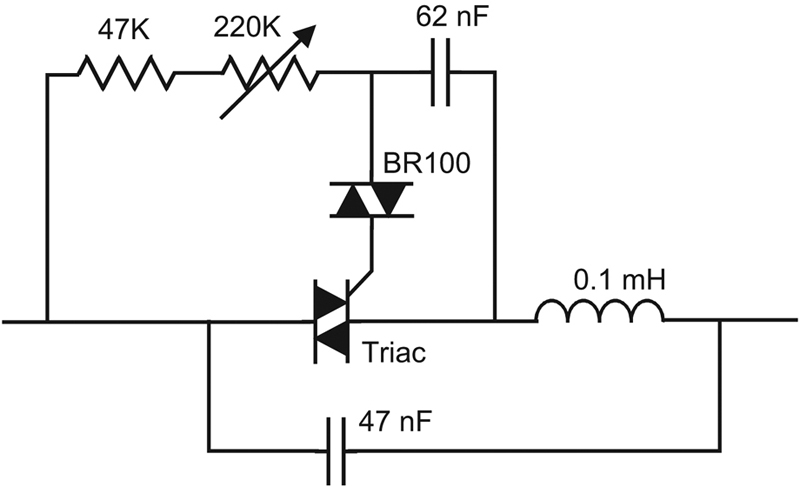
Figure 5.11 Triac Dimmer Circuit.
The input of an inactive LED driver is high impedance, with a large capacitor on the DC side of the bridge rectifier. The capacitor across the triac allows a small current to flow through the bridge rectifier and the smoothing capacitor starts to charge. When the voltage builds up, the LED driver will try to operate. The result is an occasional flicker of the LED.
What is required is a discharge circuit, to keep the smoothing capacitor voltage below that required to start the LED driver. A 390-Ω resistor was found to keep the smoothing capacitor voltage below 5 V. To prevent high power loss when the circuit is active, a simple voltage detector can be used to disconnect the 390-Ω resistor when a voltage above about 8 V is detected. This circuit is shown in Fig. 5.12.

Figure 5.12 Smoothing Capacitor Discharge Circuit.
The triac needs to see a load. Once a triac is triggered, it is the load current that keeps it switched on; the triac is a self-sustaining switch. However, an LED driver provides no load until the input voltage has risen above the LED voltage, and it takes a little time for this current to be stable at sufficiently high level to keep the triac turned on. For this reason, an additional load must be switched across the LED driver input at low voltages.
Tests have shown that a 2K2-Ω resistor works as a triac load and that it should remain in circuit until the supply voltage has risen to about 100 V, but should then be switched off until the rising edge of the next half-wave. A latching circuit to provide this function is shown in Fig. 5.13.

Figure 5.13 Additional Load Switch.
These circuits can be combined. The voltage detector for the smoothing capacitor discharge circuit can also be used to provide an enable signal for the LED driver (PWM input). Thus when the triac is off, the LED driver is also off. The combined circuit is shown in Fig. 5.14.

Figure 5.14 Complete Phase-Dimmable LED Driver.
5.9. Double Buck
The double buck is an unusual design, as shown in Fig. 5.15. It uses one MOSFET switch, but two inductors (L2 and L3) in series. Diodes steer the current in L2, which must operate in discontinuous conduction mode (DCM) for correct operation.

Figure 5.15 Double Buck.
The double buck is used when the output voltage is very low and the input voltage is high. An example is driving a single power LED from an AC supply line. A single buck stage cannot work easily because the on-time of the buck converter is too small, unless a very low switching frequency is used. One disadvantage of the double-buck circuit is that neither side of the LED is connected to a power rail. This means that during switching there is a high common-mode voltage on the LED (the voltage on both sides of the LED rises and falls at high frequency, relative to the power rails). This common-mode signal can generate high levels of EMI radiation.
Assume the maximum duty cycle, Dmax, is less than 0.5; also assume that the first stage (L2) is in boundary conduction mode (BCM) at Dmax. BCM means that the current through the inductor only just falls to zero and the next switching cycle begins.

or transposed, this becomes:

This assumes that L2 is in BCM and L3 is in continuous conduction mode (CCM); at the minimum operating input voltage (Vin min).
The storage capacitor voltage at Vin min and Dmax is given by the equation:
The peak current through the input stage inductor, at Vin min equals:

Thus the primary stage inductor L2 has a value given by:

The transfer ratio for a DCM buck converter (where R is load resistor seen by the converter), is given by:

The resistor R seen by the first stage (and assuming second stage is in CCM) is given by:

Combining the previous two equations (which turn out to be a constant):

we find that D is inversely proportional to Vin:

And we can now show that the peak inductor current through L2 is a constant over the operating input voltage:
K’ is a constant, since Vo is constant.

We can now define the average input voltage as the maximum input voltage  and the minimum operating input voltage:
and the minimum operating input voltage:

The storage capacitor value is computed based on 10% voltage ripple on the capacitor at Vin min and Dmax:

The voltage across the storage capacitor, with average voltage input, is given by:
We can now compute the average duty cycle (at average input voltage):

Computing the value of L3:

5.10. Buck Design Mistakes
5.10.1. Common Errors in Low Voltage Buck Design
1. Using an inductor that has too high inductance.
Although increasing the inductor value may seem to be the answer to reduce current ripple, it actually causes problems because the current does not fall enough between switching cycles for proper control by the controller IC. The voltage seen across the current sense resistor at switch-on will be almost at the current sense comparator reference voltage. At switch-on there will be a current surge, caused by the flywheel diode reverse current and the current through the inductor’s parasitic capacitance. The smallest current surge will create a voltage spike across the current sense resistor and hence the current sense comparator will trip. This means that the MOSFET will switch off almost immediately after switch-on.
A typical switching pattern is one proper switching cycle, where energy is stored in the inductor, followed by one short switching pulse. This switching pulse provides very little energy to the inductor, but generates high switching losses. The result is a less efficient circuit that could suffer from overheating and EMI problems
2. Using the wrong type of flywheel diode.
A Schottky diode has a low forward voltage drop, which will give low power dissipation. However, in low duty cycle applications the LED current is flowing in the flywheel diode most of the time. A forward voltage of say 0.45 V at 350 mA results in 157.5 mW conduction losses, so an SMA size package works well, but for higher current applications a large SMB or SMC package should be considered. Note that the forward voltage drop of Schottky diodes increases with their current rating, so a 30 V Schottky has much lower Vf than a 100 V Schottky.
5.10.2. Common Errors in AC Input Buck Circuits
1. A common error is trying to drive a single LED from the AC mains supply.
The duty cycle is Vout/Vin, so for universal AC input 90–265 V AC, the rectified voltage is about 100–375 V. The worst case is the higher voltage; consider driving a white LED with 3.5 V forward voltage. The duty cycle will be 3.5/375 = 0.9333% duty cycle. If the switching frequency is 50 kHz, with 0.02 ms period, the MOSFET on-time will be just 186 ns. This time is too short for the current sense circuit to react; it needs to be at least 300 ns. Operating at 20 kHz will give an on-time of 466 ns, which is near to the limit for accurate control. A double buck (described in Section 5.9) may be needed.
2. Another error is not taking into account parasitic capacitance of the inductor windings and reverse current in the flywheel diode.
These factors can be ignored in low to medium voltage DC applications, but not in applications where the supply voltage is more than about 200 V. The current peak through the MOSFET at turn-on can be high enough to trip the current sense circuit, resulting in erratic switching. An RC filter between the current sense resistor and the current sense input of the integrated circuit may be necessary. A 2.2 kΩ series resistor followed by a 100 pF shunt capacitor to ground should be sufficient.
3. Trying to operate a fixed frequency buck circuit (peak current mode control) with a duty cycle above 50% will result in instability.
The switching frequency will jump to half the nominal value, known as subharmonic switching. However, there is a simple solution: if the load voltage is more than 50% of the supply voltage, constant off-time switching should be used. In the case of the HV9910, this is achieved by connecting the timing resistor to the Gate pin instead of to ground (0 V). If fixed frequency is required, or the controller IC does not have constant off-time mode, slope compensation is required. Slope compensation is described in Chapter 10 (switch power supplies).
..................Content has been hidden....................
You can't read the all page of ebook, please click here login for view all page.