
Chapter 8
Nonisolated Power Factor Correction Circuits
Abstract
This chapter discusses the need for a good power factor and how it can be achieved by power factor correction or other means. A traditional boost converter type of power factor correction circuit, where the output is a fixed high voltage, is described first. This circuit could be used in combination with a buck constant current switching circuit to drive a string of light-emitting diodes. A more integrated boost stage and linear regulator, with a constant current output, is described. Other more exotic schemes are described, with one design example.
Keywords
power factor
power factor correction
PFC
boost
Bi-Bred
8.1. Power Factor Correction Defined
Power factor (PF) is defined as the ratio of true power in watts (W) to apparent power volt–amperes (VA). A pure resistive load has a PF of 1. But in active loads, such as light-emitting diodes (LED) drivers, the mains supply current passes through a bridge rectifier and then the DC voltage is smoothed using a large-electrolytic capacitor. As the capacitor only charges during the peaks in the AC supply cycle, the current is pulsed and nowhere near sinusoidal. Simple rectified supplies tend to have PFs close to 0.5.
Special measures can be taken to “correct” a poor PF. Power factor correction, or PFC, is a term used with AC mains–powered circuits. Techniques are used to create a good PF, so that the AC current is sinusoidal and in phase with the AC voltage.
There are regulations in many countries that require a good PF. In Europe, regulations demand that residential lighting have a PF of greater than 0.7 and commercial lighting have a PF greater than 0.9. In any case, lighting products with a power rating of greater than 25 W must have a good PF of 0.95 or higher, regardless of the end use. In the United States, there are voluntary guidelines, with the DoE and Energy Star requirements being similar to Europe. The exception is the State of California that asks for a PF greater than 0.9 for all power levels of residential and commercial LED lighting.
Distortion of the current waveform reduces the PF, but also gives some harmonic distortion. There is a relationship between PF and total harmonic distortion (THD):

Electromagnetic compatibility requirements sometimes quote THD, rather than PF. In Europe, applying the limits specified by the European Normalisation, EN-61000-3-2 class C, is mandatory for lighting products.
8.2. Typical PFC Boost Circuit
The most common PFC circuit is a boost converter, where the AC line voltage is boosted to give a constant voltage of about 400 V across an energy storage capacitor. The peak amplitude of the charging current pulses into this capacitor is arranged to be sinusoidal. This is achieved by switching the current on for short but constant periods: with constant on-time switching, as the supply voltage rises and falls, so does the amplitude of the current. A typical PFC circuit using the ST Microelectronics L6562 is shown in Fig. 8.1.

Figure 8.1 Power Factor Correction (PFC) Circuit.
There are a number of controller ICs for PFC. One of the most popular has been the L6562 from ST Microelectronics. Other well-known controllers are HBD853-D (On-Semiconductor), UCC29019 (Texas Instruments), LT1249 (Linear Technology), and FAN7350 (Infineon).
A simple alternative is to use a fly-back supply, see Section 8.3. It is common to switch the primary current off when a certain current level is reached, but this leads to constant average current. To give a good PF, the primary current should be switched with a constant “on-time,” so that the current amplitude rises and falls in phase with the supply voltage. The secondary current will rise and fall at double the AC line frequency and so a large secondary capacitor is required to absorb this ripple, to prevent significant ripple in the output voltage.
Driving a LED from the output of a PF-corrected supply usually requires a simple buck converter, as the voltage source tends to be very high (about 400 V). However, alternative solutions exist; these are the Bi-Bred and the buck–boost–buck (BBB). Both of these topologies can be driven using an HV9931 IC from Microchip, see Sections 8.5 and 8.6. The advantage of using a simple buck regulator from a constant voltage supply is that there will be no low-frequency ripple current through the LEDs, which would be at double the AC mains frequency, so 100 or 120 Hz.
8.3. Boost–Buck Single Switch Circuit
The boost–buck single switch circuit is also known as a fly-back circuit. Fly-back circuits are described in more detail in Chapter 9, but this section is specifically considering their use as direct LED drivers with PFC. In the case of fly-back circuits, constant on-time switching is required in order that the input current follows the sinusoidal input voltage.
The schematic given in Fig. 8.2 was adapted from an On-Semiconductor application note AND9043/D. It shows how an On-Semiconductor NCP1014 can be used to drive an LED load of 35–80 V; typically 10–22 LEDs connected in series. Only a few critical parts are numbered, a more detailed explanation is offered further.

Figure 8.2 Buck–Boost Light-Emitting Diode (LED) Driver with PFC.
The NCP1014 has a high-voltage switch between pin 3 and pin 4 (0 V). The switch turns on for a constant period and the inductor is charged. Then when the switch turns off, current continues to flow through L1 via diode D1, charging the output capacitors C9 and depleting the inductor’s energy. Once the voltage across C9 is sufficiently high, current will flow through the LEDs. The current flow causes a voltage drop across R10; this voltage is then used to provide feedback to the control IC. Feedback is via a photocoupler; the voltage across R10 feeds a potential divider R11 and R14 to drive a small current through the photocoupler’s LED. When the corresponding phototransistor turns on, pin 2 of the NCP1014 is pulled low and the switching is disabled.
In addition, if the LEDs become open circuit, some protection is needed to prevent damage of C9 (which could explode) and burning of components. If the output voltage rises above the nominal 90 V of the protection circuit Zener diodes, Z1–Z3, current flows into the photocoupler’s LED. The switching is disabled, as before.
The circuit shown in Fig. 8.2 will produce light with almost 100% low-frequency ripple (100 or 120 Hz) because there is very little energy storage in capacitor C9. When the AC mains voltage is close to the zero crossing point, there will be no light from the LEDs. This prevents such driver circuits from being used in applications, such as traffic lights, where the high level of low-frequency ripple would interfere with the associated safety camera. This is because the frame scan rate of a camera is close to 100 Hz and the resultant image would show a flicker effect.
8.4. Boost–Linear Regulator Circuit
One technique used in many high-power LED lamps, such as streetlights, is to boost the voltage to about 400 V using a PFC stage as described at the beginning of this chapter. The current is limited, but not controlled. To control the current and drive the LEDs, simple buck switching regulators can be used to provide a constant current source.
An alternative, to be described in this section, is to boost the voltage and then use a linear regulator to control the LED current. To achieve good efficiency, the system has to be designed carefully. As boosting universal AC mains voltages results in typically 450 V being produced, the LED forward voltage drop must also be about 440 V, to leave 10 V across the linear regulator. To achieve such a high-forward voltage drop, a lot of LEDs must be connected in series (typically 120–140 LEDs are needed).
With a high number of LEDs, the forward voltage tolerance will also be significant. If the boost stage voltage was 450 V and the total voltage drop of the LED string was of a similar voltage, due to a batch of LEDs with particularly high-forward voltage drop (Vf), the LEDs would be dim or would not light. To overcome this, the output voltage of the boost stage needs to be adjusted automatically so that the required LED current is reached.
Conversely, if the total forward voltage of the LED string were lower than expected, the voltage drop across the linear regulator would be higher and hence, the power dissipation could be too high. Again, an output voltage control of the boost regulator, so that the voltage drop across the linear regulator is as low as possible, will solve this problem.
One such circuit to perform the functions described above is the HV9805 from Microchip. A typical schematic using the HV9805 is given in Fig. 8.3.

Figure 8.3 Boost–Linear Regulator Using HV9805.
The boost section of the circuit uses a 600-V MOSFET, M1, in a cascade connection. The gate of M1 is connected to an 18-V supply, comprising R1, R2, Z1, and C4, powered from the rectified mains. There is an internal MOSFET connected between pin 10 and pin 1 (GND), which drives the source of M1 to ground and turns it on. The internal MOSFET thus never sees more than 18 V across its drain and source, allowing low-voltage (and low-cost) silicon processes to be used.
The MOSFET switching is controlled by monitoring the voltage across R8, which returns the ground connection to the bridge rectifier. The CSH and CSL pins are differential inputs used to sense the current. After the MOSFET M1 turns off, there will be some ringing at its drain. The circuit needs to detect when the ringing has stopped, before it starts the next switching cycle, otherwise the PF could be affected. However, when the AC input voltage is low, near to the zero crossing point, the ringing is difficult to detect. The addition of C9 (with a small damping resistor R18 in series) increases modulation of the sense voltage, to improve detection at these times.
The linear regulator at the output uses an external 300-V MOSFET M2. The voltage rating can be lower than the high-voltage rail because most of the output voltage drops across the LEDs. Resistor R13 is the output current sense resistor. The voltage across M2 is monitored by the potential divider R6 and R7 and input to pin 4 (HVS). The voltage on pin 4 is proportional to the headroom voltage on the linear regulator, and is adjusted by controlling the output of the boost stage.
8.5. Bi-Bred
The Bi-Bred is very similar to the Cuk boost–buck that was described in the previous chapter (see Fig. 8.4).

Figure 8.4 Bi-Bred Circuit.
PWM, Pulse width modulation.
PWM, Pulse width modulation.
The main difference between the Cuk and the Bi-Bred is that, in a Bi-Bred, the input inductor is in discontinuous conduction mode (DCM) and operation of the output stage in continuous conduction mode (CCM). The energy stored in each inductor is proportional to the inductance value. This means that in the design, the input inductor L1 must have a small enough energy stored to ensure that conduction stops before the end of each cycle. Consequently, the input inductor value must be relatively small. The output inductor L2 must have large enough energy stored (large-inductance value), so that the current only falls to about 85% of its nominal value at the end of each switching cycle.
When power is first applied, MOSFET M1 is off and waiting for the first clock signal to trigger the gate drive pulse. At this time, the storage capacitor C3 immediately begins to charge from the supply voltage through D1 and L1. The voltage across C3 will not rise very high though because, when the MOSFET M1 switches on, the charging current is redirected to the 0-V rail. With M1 conducting, current continues to rise in amplitude through the inductor L1 until the voltage drop across R2 is sufficient for the input current feedback comparator inside the HV9931 to trigger, which turns M1 off. Now the input circuit acts like a boost converter because the current through L1 cannot change immediately and it charges C3 to a high voltage.
The next time that M1 switches on, energy stored in C3 is used to drive current through the LED load. The current rises in inductor L2 and the load until the voltage drop across resistor R7 is sufficient to trip the HV9931’s output current sense comparator and turn M1 off again. The current flow through L2 passes through D2 to keep current flowing in the LED load. Notice that the current sense resistor is not in this path because the current level measurement is not required until the MOSFET turns on again. Having the current sense resistor outside the flywheel diode path minimizes power loss.
The output of the Bi-Bred is configured as a buck stage. Energy is supplied from a bulk storage capacitor, C3. This capacitor has a sufficiently large capacitance value to provide a more or less constant supply voltage over an AC line cycle period. A constant capacitor voltage supplying power to the buck stage means a constant switch duty cycle when it is driving the LED load. The Bi-Bred draws an approximately sinusoidal AC line input current when driven from a switch operating at constant duty cycle, hence a large capacitance value for C3 helps to produce a good PF.
The duty cycle of the switching is given by  .
.
.Or put another way,  . So if Vin = 350 V and Vo = 3.5 V (a typical white LED),
  . Such a small duty cycle can be difficult to switch properly, as we have seen for a buck converter. This means that a Bi-Bred is not really suitable for driving short LED strings.
. So if Vin = 350 V and Vo = 3.5 V (a typical white LED), . Such a small duty cycle can be difficult to switch properly, as we have seen for a buck converter. This means that a Bi-Bred is not really suitable for driving short LED strings.8.6. Buck–Boost–Buck
The buck-boost-buck (which we will refer to as BBB) is a proprietary circuit, patented by Supertex (now Microchip), and is illustrated in Fig. 8.5. It resembles the Bi-Bred in some respects, except for two current-steering diodes, D1 and D4.

Figure 8.5 Buck–Boost–Buck (BBB) Circuit.
Like the Bi-Bred, the input inductor is in DCM and operation of the output stage in CCM. The energy stored in each inductor is proportional to the inductance value. This means that in the design, the input inductor L1 must have a small enough energy stored to ensure that conduction stops before the end of each cycle. Hence the input inductor value must be relatively small. The output inductor L2 must have large enough energy stored (large-inductance value) so that the current only falls to about 85% of its nominal value at the end of each switching cycle.
When power is first applied, MOSFET M1 is off and waiting for the first clock signal to trigger the gate drive pulse. At this time, the storage capacitor C3 is not charged. With M1 conducting, current begins to rise in amplitude through the inductor L1 until the voltage drop across R2 is sufficient to trip the HV9931’s input current sense comparator, which turns M1 off. Now the input circuit is in flywheel mode because the current through L1 cannot change immediately and it charges C3 to a moderately high voltage. The voltage across C3 is typically midway between the input and output voltage levels.
The energy in C3 is used to drive current through D2, L2, and the LED load the next time that M1 switches on. The current rises in inductor L2 and the load until the voltage drop across resistor R8 is sufficient to trip the output current sense comparator and turn M1 off again. The current flow through L2 passes through D2 to keep current flowing in the LED load. Notice that, like in the Bi-Bred, the current sense resistor is not in this path because the current level measurement is not required until the MOSFET turns on again; this minimizes power loss.
The output of the BBB is the buck stage. Energy is supplied from a bulk storage capacitor C3, with sufficiently large capacitance to provide a more or less constant supply voltage over an AC line cycle period. A constant capacitor voltage across C3, which supplies power to the buck stage, means a constant switch duty cycle when it is driving the LED load. The BBB draws a more or less sinusoidal AC line input current when driven from a switch operating at constant duty cycle. Hence, like the Bi-Bred case, a large-capacitance value for C3 helps to produce a good PF.
In practice there is a limit to the value of C3 because of physical size, particularly if plastic film capacitors are used. This means that there will be some voltage ripple across C3, at a frequency double that of the AC line (i.e., 100 Hz when driven from a 50-Hz supply, or 120 Hz when driven from a 60-Hz supply). The effect of this ripple voltage is to generate secondary harmonic signals in the input current, which reduces the PF. By adding a simple circuit, the second harmonic can be reduced; the MOSFET off-time is modulated by the ripple voltage and this acts like a negative feedback to reduce the second harmonic. The additional circuits are usually used only if plastic film capacitors or small-value electrolytic capacitors are used for C3 and are shown in Fig. 8.6.

Figure 8.6 BBB With Harmonic Reduction.
When MOSFET M1 is conducting, there is a current path from C3 through D10 and D2 to charge C11 (with a negative voltage at the anode of D3 and positive at the anode of D9). When MOSFET M1 turns off, so that D3 is conducting the LED current, the voltage across C11 can forward bias D9 and charge capacitor C5. Between each switching cycle, resistor R7 discharges capacitor C5. Thus the ripple voltage across C3 will modulate the average voltage across C5. Capacitor C7 acts as a DC block, to allow just the modulation across C5, rather than any DC level, to vary the MOSFET off-time. As the voltage across C5 rises and falls, current through R6 rises and falls, thus shortening or lengthening the off-time in proportion to the AC mains voltage.
The duty cycle of the switching in a BBB converter is given by  .
.
.Or put another way, 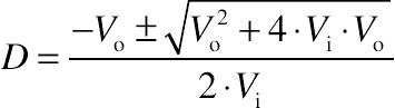 . So if Vin = 350 V and Vo = 3.5 V (a typical white LED),
 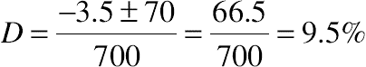 . This is a considerably greater duty cycle than either the Bi-Bred or the buck converter with a similar low-voltage load. This means that the BBB converter is most suitable for driving short LED strings.
. So if Vin = 350 V and Vo = 3.5 V (a typical white LED), . This is a considerably greater duty cycle than either the Bi-Bred or the buck converter with a similar low-voltage load. This means that the BBB converter is most suitable for driving short LED strings.8.6.1. Buck–Boost–Buck Design Equations
The HV9931 is a peak current control IC that is designed for controlling the nonisolated single-stage PFC converter (BBB) described earlier. A typical application circuit of the HV9931 was shown in Fig. 8.5, but is redrawn with different component annotation to help with the further description, in Fig. 8.7.

Figure 8.7 BBB-Annotated Circuit.
The HV9931 has a built-in high-voltage regulator circuit producing 7.5 V ± 5% at VDD, hence making the circuit relatively simple because we do not have to consider separately powering the integrated circuit.
As soon the start-up threshold is reached at VDD, an internal oscillator circuit is enabled. The oscillator circuit is actually three functions: a timer, a latch, and a latch-reset circuit. The timer is a current mirror that charges an internal capacitor; when the threshold of 0.63 VDD is reached (after RT × C seconds, where C is the internal capacitor) the latch is triggered. At this time, the timer capacitor is discharged ready for the next cycle. The output signal of the latch turns on the GATE output and switches on the power MOSFET Q1. The oscillator circuit also includes two comparators; if either of these is triggered, the latch is reset and the MOSFET Q1 turns off.
The timer uses a current mirror, with one-half connected to the RT pin. The current mirror needs a small current to flow to ground (0 V) from the RT pin, which causes the other half of the mirror to charge an internal timing capacitor. This means that the timer can be programmed with a single resistor connected to RT for either constant switching frequency or fixed off-time operation.
In the constant frequency mode, a constant timing current is required, so the timing resistor must be connected between the RT pin and 0 V. In the fixed off-time mode, the timing resistor must be connected between the GATE and RT pins; current flow (and hence timing) only begins when the GATE pin is at 0 V. Thus the timer will set the latch and turn on the MOSFET after a programmed time period following the turn-off of the GATE output.
The fixed off-time operating mode is preferred because it: (1) reduces the voltage stress at C1, (2) improves input AC ripple rejection, and (3) inherently introduces frequency jitter that can help reduce the size of the input EMI filter required. Hence we will use the fixed off-time mode for the following design.
Connecting the resistor from RT to GATE programs constant off-time:
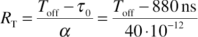
Where α = 40 pF, τ0 = 880 ns.
In terms of RT, this transposes to:
The input and output feedback comparators are used as current sense inputs, for programming peak currents in L1 and L2. Both comparators use the ground potential (GND) as a reference and can be used to monitor voltage signals of negative polarity with respect to GND. A blanking delay of 215 ns is added to prevent false tripping the comparators due to the circuit parasitic capacitance. The currents iL1 and iL2 that trip the comparators can be computed as:

Where Vref in this equation is an external reference voltage.
We will use Vref = VDD as an example. When either of the feedback comparators detects negative input voltage at its current sense (cs) input, the latch resets, the GATE output becomes low voltage.
We can easily calculate the current in L2, as the output current is more or less constant with some ripple. It is assumed to operate in CCM,
Where iL2 is the average current and ∆iL2 is the peak-to-peak current ripple in L2. Thus the constant peak current control used in the HV9931 introduces a peak-to-average error 0.5 × ∆iL2 that needs to be accounted for when programming the resistor divider Rref2/Rcs2. Fortunately, this error is nearly constant for any input voltage at fixed Toff and it is relatively small compared to iL2 (15% typical). The ripple will have a minimal effect on the overall regulation of the output current. The error is however a function of the output voltage variation and the inductance value tolerances of L2.
8.6.1.1. Choice of L1
We need to design the input buck–boost stage to operate in DCM to give a good PF. Operating in DCM at any given line and load condition will ensure low distortion of the input current and stability of the control loop. Therefore, let us assume that the current in L1 becomes critically continuous at full load and at some minimum operating AC line voltage VAC min. This boundary conduction mode (BCM) condition should normally occur at the peak of each half-wave of the input AC current. If we assume a unity PF (PF = 1), this boundary condition will then coincide with the peak input voltage VAC min. As both converter stages are in CCM at this point, the ratio between the output and the input voltage can be expressed as:

Where η1 and η2 are the corresponding efficiencies of the input buck–boost stage and the output buck stage. The overall converter efficiency equals η = η1 × η2. The duty ratio D of the switch M1 is the greatest at this condition. (Duty ratio is defined as D = Ton/Ts, where Ton is the on-time of M1, and Ts is the switching period.)
The input AC line current is a ratio of the output power to the input voltage and efficiency:

On the other hand, the peak input current must be equal to the (averaged) peak current through L1:

Where the peak current in L1 (iL1pk) is dependent on the maximum voltage across L1, the inductance and the on-time:

As we are only considering the constant off-time case, let us express this in terms of Toff = Ton × (1–D)/D.

Combining the equations (using the mean value of VAC min) and solving for the inductance value gives:

Note, that the critical inductance L1 in this equation corresponds to the boundary conduction at VAC min. The value used in practice should be lower than this, to allow for component tolerances and parasitic elements. The inductor value has some tolerance, perhaps 10%, but tolerance in all the other components and switching off-time should be considered too. If the inductance goes above the critical value, CCM will occur and the input waveform will be severely distorted. For these reasons, the value of L1 should be reduced to 63% of its maximum allowed value:
The designer must be careful when considering standard inductors for L1 or designing a custom one. As L1 conducts discontinuous current, magnetic flux excursion in the core material can cause heating. Hence the design of L1 is limited by the power dissipation in the magnetic core material rather than by the saturation current of the inductor selected.
8.6.1.2. Choosing C1
Capacitor C1 is usually an electrolytic capacitor because of the required high-capacitance value and high-voltage rating. This is sometimes a cause for concern about reliability. However, the lifetime rating of electrolytic capacitors has improved in recent years and lifetime ratings of 10,000 h at 105°C are available from multiple sources. Considering that the lifetime doubles for every 10°C drop in temperature, this equates to 40,000 h at 85°C. So at reasonable temperatures, the lifetime of the electrolytic and the LED are comparable.
Capacitor C1 is the main energy storage element and its capacitance value significantly affects the distortion of input current. The minimum capacitance value of C1 is determined by the input harmonics limits required for a specific application. Lighting products are sold in large quantities, and thus these high-volume products can potentially have a high impact on the low-voltage public supply system. The European EN 61000-3-2 class C limits are applicable to lighting products and are comparable to the limits imposed by ANSI C82.77 standards in the US market. These restrict THD to approximately 33%. Both, the class C and ANSI standards limit the third harmonic current of lighting products to ∼30%. The regulations for LED-based traffic signal heads are generally stricter and require THD to be less than 20% (ITE VTCSH Part 2).
The main component of the AC ripple voltage across C1 is the second AC line harmonic. This ripple causes modulation of the duty cycle, D(t), given by the following equation:

Where VC(t) is voltage across C1 at any time t.
Combining the equations developed in Section 8.6.1.1, we have an equation for the input AC current:

In terms of a sinusoidal waveform, this becomes:

Where fAC is the AC line frequency (50 or 60 Hz).
Assume that a small second harmonic ripple voltage VC exists across C1, i.e. 100 or 120 Hz, so that the voltage at C1 can be written as:
Where iC/VC << 1. By substituting across these last three equations we will produce a displaced fundamental term and a third harmonic term in the AC line current. It can be shown from the resulting equation that the third harmonic distortion of the input AC line current for a given relative second harmonic ripple KC = iC/VC << 1 is:
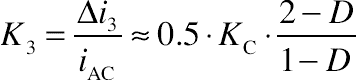
Thus every 1% of second harmonic ripple at C1 will generate at least 1% of third harmonic component in the AC line current even when the duty cycle is small.
Now we can find the capacitance value of C1 needed to limit the third harmonic distortion to some given constant K3. Equations used to find L1 can now be used to solve for the duty cycle D at any VAC within the operating range.

This is a bit unwieldy, so let us introduce a parameter δ as follows:

Now the equation for the duty cycle looks much simpler:

We can rewrite the equation for the third harmonic ripple K3 as:

Recalling that D = Vo/(η2 × VC) and using D = 2 (√(1+δ)−1)/δ from above, we can determine the voltage at C1 for a given VAC:

We have assumed that KC = iC/VC << 1. This condition is met if the value of capacitor C1 large enough, so that the AC ripple voltage across C1 is low. Therefore, C1 decouples the bulk of the AC ripple current at the output of the input converter stage. Averaged over a switching cycle, this current can be written as:

The AC line current iAC(t) has been given by a previous equation. Based on the assumptions made earlier, the AC component of i2(t) contains second harmonic current only. This AC current in C1 can be expressed as:
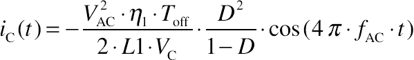
Substituting D and VC (using δ from the condensed equations earlier) gives:

Relative ripple voltage at C1 can be calculated as KC = iCpk × ZC/VC, where iCpk is the amplitude of iC(t) and ZC = 1 /(4π × fAC × C1) is the impedance of C1 at 2 × fAC. Substituting VC we obtain:

Solving this equation for C1 and substituting for KC we get:

The RMS value of the switching current in C1 can be calculated using the following equation:

The RMS value of the second AC line harmonic is:

8.6.1.3. Calculating L2
Calculating the value of the output filter inductor L2 is simple. The designer must decide on the allowable amount of switching ripple current in L2. Then:

Where ∆iL2 is the peak-to-peak current ripple in L2. Larger values of L2 will produce smaller ripple ∆iL2, and therefore smaller peak-to-average error in the output current control loop. However, low-amplitude feedback signals would also make the output current sense comparator more susceptible to noise. It is a good practice to design L2 for ∆iL2 = 20–30%. The reason for having moderate inductor current ripple is to allow a sufficiently high-feedback signal for the current sense comparator. An output capacitor connected across the LED load can be added, to reduce the output ripple current further, if needed.
Unlike the design of input inductor L1, the design of L2 is typically limited by the saturation flux of its magnetic material. However, power dissipation due to the core loss may also need to be considered. The saturation current rating of the inductor must satisfy:
8.6.1.4. Power semiconductor components
Now we can calculate the voltage and the current ratings of the MOSFET M1 and the rectifiers D1–D4.
8.6.1.4.1. MOSFET M1
The current in M1 is composed from the currents in the inductors L1 and L2. Hence, the RMS current in M1 can be computed as:

Where iL1pk and Dmax are calculated at VAC min. We can disregard the ripple current in L2, as we want the average current. The drain voltage rating of M1 can be determined as:
Where VC max and KC are calculated at VAC max.
For the power MOSFET M1, it is very important to find a good balance between the total gate charge Qg and the on resistance RDS (ON). Using a MOSFET with low RDS (ON) will not necessarily achieve greater efficiency. The gate drive current from the HV9931 is limited, so a large-gate charge will slow down the switching time and thus increase switching losses.
In addition to the slow turn-on speed generating higher-switching power loss, MOSFETs with high Qg will require more current from the HV9931’s internal voltage regulator. When a MOSFET is being switched, the average current required by the gate driver is given by: ig = Qg × fSW. So, if we have a MOSFET with 30-nC gate charge being switched at 50 kHz, the average gate driver current is 1.5 mA. A small-additional current is required by the HV9931 internal bias circuits, so we could have 2 mA drawn from the internal high-voltage regulator, while dropping 300 V or so. The HV9931 gate driving capability is therefore also limited by the package power dissipation. Being a linear regulator, the power dissipated will be iin × (Vin – VDD). Thus nonoptimal selection of M1 may cause the HV9931 to overheat.
8.6.1.4.2. Diodes D1–D4
The highest currents in D1–D4 averaged over the AC line cycle can be calculated as:

Where δmax and δmin are calculated from our definition of δ given in Section 8.6.1.2, at VAC max and VAC min correspondingly. Peak currents in D1 and D4 equal to iL1pk are calculated using the value of δ at VAC min. Peak currents in D2 and D3 are computed as io + 0.5 × ∆iL2.
The voltage ratings for D1–D3 are given as:

Using ultrafast recovery rectifiers for D2 and D3 is essential for good efficiency of the LED driver. Both diodes operate at high current and are subjected to fast transitions and high-reverse voltage.
The required reverse voltage rating of D4 depends on several factors. During the dead time, there could be a significant postconduction resonance. The LC tank is formed by L1 and the parasitic capacitance of D1, D4, and M1. The resonant period can be estimated as:

Where COSS is the output capacitance of M1, and CJD1 and CJD4 are reverse-biased junction capacitances of D1 and D4 correspondingly.
Due to a finite reverse recovery time of D1, the input inductor L1 develops a certain reverse current in the beginning of the dead time. As L1 runs in DCM, the reverse recovery time of D1 has negligible effect from the overall power efficiency point of view. However, even a small reverse current in L1 can cause a very high-voltage spike across D4, when both diodes stop conducting. Thus, ultrafast recovery diode is recommended for D1.
As CJD4 << COSS typically, the postconduction oscillation occurs mainly across D4. The drain voltage of M1 will remain almost unchanged throughout the dead time. Besides causing the high-voltage stress across D4, this oscillation may affect the EMI performance of the circuit. Thus, adding an RC snubber circuit across D4 is recommended. If the snubber capacitance value is greater than (COSS + CJD1), the reverse voltage rating of D4 can be reduced significantly.
The snubber capacitor can be selected as (approximately)
And the snubber resistor

The snubber resistor should be rated at 0.5 or even 1 W, and 500 V breakdown. The minimum voltage rating for D4 will then be:
Thus in theory a fast 400-V diode can be used for D4 in a universal 90–260 V AC LED driver. In practice a fast diode rated at 600 V is normally used.
8.6.1.5. Output open circuit and input undervoltage protection
The BBB circuit is a constant output current source. Hence it can generate destructive voltage at its output in the case of an open circuit condition. A simple circuit shown in Fig. 8.8 protects the HV9931 LED driver from the output overvoltage.

Figure 8.8 Output Overvoltage Protection.
Zener voltage of D12 greater than the maximum output voltage must be selected. Resistor Rov is typically 100–200 Ω. However, it will affect the output current divider ratio and needs to be included in the calculations by replacing Rcs2 by (Rcs2 + Rov).
Note, that the open circuit condition can create an overvoltage across C1. This voltage stress can be limited by connecting a Zener diode or TVS across C1 limiting the voltage to some acceptable level greater than VC max. The power dissipation in this voltage clamp device is usually small, as the HV9931 operates at minimum duty cycle during the open circuit condition.
The HV9931 inherently protects the LED driver from an input undervoltage condition by limiting the input current. However, increased input current may generate excessive power dissipation in L1, D4, M1, and Rcs1. Additional protection is recommended by connecting a Zener diode in series with the Vin pin of the HV9931, as shown in Fig. 8.9. When the input voltage drops so that the Zener diode stops conducting, the HV9931 no longer has power and turns off.

Figure 8.9 Input Undervoltage Protection.
In addition, an improved input undervoltage protection circuit is shown in Fig. 8.9, which can achieve better performance compared to the simple fixed input current limiting. The reference for the CS1 comparator is derived from the input rectified AC waveform. The voltage divider ratio of R1:Rref1 is programmed such that the Zener diode Zref1 clamps the divider voltage at any input greater than VAC min, that is:

When the input voltage falls below VAC min, the reference voltage will reduce too, preventing the inductor L1 from entering CCM. Operating L1 in CCM can cause undesirable LED flickering, audible noise, and excessive heat dissipation due to the loop oscillation. Rbias creates a positive offset voltage to maintain the reference above 0 V during the AC line voltage zero crossings and thus prevents interruptions of the output current.
8.6.1.6. Surge immunity and EMI considerations
High-voltage surges occur on the AC power mains as a result of switching operations in the power grid and from nearby lightning strikes. LED lighting and signal equipment may be subjected to surge immunity compliance testing in accordance with various standards (EN61000-4-5, NEMA TS-2 2.1.8, etc.) to ensure its continued reliable operation if subjected to realistic levels of surge voltages. The BBB LED driver circuit relies mainly on the transient suppressors (MOV and TVS) to protect it from the input AC line surge. There is little capacitance available at the AC input of the LED driver to absorb high-surge energy, although the EMI filter inductors do slow down any fast transient edges. Thus a transient suppressor needs to be connected across the AC input terminals.
As with all switching converters, selection of the input filter is critical to obtaining good EMI. The HV9931 solution using fixed off-time switching provides an inherent advantage of the frequency dither (spread spectrum). Hence less filtering may be needed, resulting in a smaller EMI filter.
Some important guidelines for PCB design must be followed for optimal EMI performance of the BBB power converter. The area of the fast-switching current loops must be minimized. The first loop including of M1, C1, D2, and D3 can significantly degrade the overall EMI performance due to the reverse recovery current in D3. Using a very fast diode is recommended for D3. The second loop consists of Cin, D1, C1, M1, and Rs1. As the input buck–boost stage runs in DCM, the reverse recovery current in D1 is insignificant. However, charging its junction capacitance can generate fast-current transients. The large physical dimensions of C1 can complicate optimal routing of these loops.
Optimal routing of the HV9931 gate drive output loop can be important for EMI performance, as well as for preventing destructive oscillations of the M1 gate voltage. Adding a 100R resistor in series with the gate will help to dampen any oscillations caused by parasitic inductance and capacitance. The gate driver loop area must be minimized to keep the inductance low and to reduce the emissions from the loop antenna created. The PCB trace connecting the source terminal of M1 with the GND pin of the HV9931 must be as short as possible to reduce inductance. The VDD bypass capacitor, CDD, provides the current for the MOSFET gate drive signal; it must have low ESR and located close to the VDD pin of the HV9931.
Postconduction oscillation across D4 during the dead time of L1 can be another substantial source of RF emission. Adding a snubber circuit (Rd and Cd) can help significantly. In addition, this snubber is needed to reduce the voltage stress at D4 as discussed in Section 8.6.1.4.
The outside case of an electrolytic capacitor is connected to its negative terminal and in a traditional power supply this terminal is normally connected to the ground (0 V) rail to provide a degree of shielding. However, in the BBB circuit, this is not possible because the central energy storage capacitor C1 in this circuit is “floating” (not connected to circuit ground). It will behave like a radio frequency antenna. Placing the whole circuit into a shielded enclosure of some type is most likely necessary in the majority of applications.
8.7. LED Driver Design Example Using the BBB Circuit
Let us design a power converter for driving LEDs with the following characteristics:
Input AC line voltage: 80–260 V AC, 50–60 Hz
Output current: 350 mA
Output current ripple: ±15%
Output voltage: 35 V (max.)
THD: <20% at 120 V AC
Off-time: 15 μs
We will assume that the efficiencies of the input buck–boost stage and the output buck stage are η1 = 0.85 and η2 = 0.9 correspondingly. The efficiency of a DCM buck–boost stage is typically lower compared to the CCM buck stage. The overall efficiency η = η1 × η2 ≈ 0.76.
Note that a “universal” 80–260 VAC input range is not recommended, because of the high stresses on the components. Two designs, one covering 80–135 VAC and the other covering 150–260 VAC, would be the preferred option.
Step 1. Using the equation given earlier for Toff, we will calculate the timing resistor RT value for Toff = 10 μs.

Using the nearest standard resistor value, RT = 360K.
Step 2. We will allow 30% peak-to-peak switching current ripple in L2, or ∆iL2 = 0.3iL2 = 0.105 A. Then the peak current in L2 is
The value of L2 can be calculated from

L2 = 4.7 mH is a standard value.
The DC current rating of L2 equals to io = 0.35 A. The saturation current rating of this inductor must be higher than the peak current.
Step 3. Assuming a 0.25-W power dissipation in the output current sense resistor Rs2, we can calculate its value.

We will select a 1 Ω, 0.25 W resistor for Rs2, to minimize the power loss.
We can now calculate the value of Rcs2. Let us use the VDD pin as a reference voltage (VDD = 7.5 V). Although VDD is reasonably accurate, it may drop during the AC line voltage cusps when there is no input voltage available at Vin, if the VDD capacitor is too small to hold up the voltage. An external voltage reference is needed for better accuracy. Selecting Rref2 = 100K, we can calculate the value of Rcs2 using the equation:
, which transforms to

Rcs2 + Rov = 5.366 kΩ, let Rcs2 =5.1 kΩ and Rov = 270 Ω.
Step 4. The input inductor L1 is assumed to reach BCM at VAC min at the peak of the input voltage hump. We can calculate the critical inductance value that meets this condition.

This is the maximum value, so we need to choose a lower inductance. Let L1 = 700 μH.
Step 5. Let us calculate the parameter δ and the duty cycle D at VAC min, VAC max, and VAC using the equations:
Case 1, VAC min = 80 V AC:

Case 2, VAC max = 260 V AC:

Case 3, VAC at 120 V AC:

Step 6. The maximum peak current in L1 will occur at VAC min. It can be calculated from:

Note that most “off-the-shelf” 700-μH DC chokes may be not suitable for L1. As the current in L1 cycles from zero to as high as iL1pk every switching cycle, there may be excessive power dissipated in the magnetic core of L1 due to a large-magnetic flux excursion. On the other hand, the wire gauge used in such inductors is selected based on its DC current rating, whereas the RMS current in L1 is substantially lower than its peak current, so thin wire can be used. Thus, a custom designed L1 is likely to produce a more size-efficient solution. This makes prototyping more difficult, but in volume production there will be little impact in terms of cost.
Step 7. The next step is calculating the input current sense and divider resistors Rs1 and Rcs1. Let us allow 0.1 W of power dissipation in Rs1 at VAC min. Power dissipation in Rs1 can be calculated as:

Solving this equation for Rs1, we obtain:

Let us select Rs1 = 0.47 Ω, 1/4 W. To calculate Rcs1, we will use the equation

This is assuming Vref = VDD and Rref1 = 100K as before. We will program the peak input current limit as 120% of iL1pk, so that Rcs1 is increased by 20%. Then,
Step 8. Let us assume the third harmonic distortion coefficient K3 = 0.15 at VAC = 120 V AC, 60 Hz. Then, the equation for the value of C1 is:

Using the next equation at VAC = 260 V AC, we can calculate the required voltage rating of C1.

The voltage ripple at C1 is small at high-input voltage and can be ignored.

We would choose a voltage rating that gives some margin to allow for input voltage surges, so a 400-V rated capacitor is the next highest available rating.
The switching ripple current rating for this capacitor can be calculated at the minimum input voltage (80 V AC).

The RMS value of the second AC line harmonic is:

A 10 μF, 400 V capacitor rated for 0.51 A ripple current would be suitable.
Step 9. Optimal selection of the switching MOSFET M1 is based on finding a good balance between the total gate charge Qg and the on-resistance RDS (ON). The drain voltage rating is given by the equation:

An 800-V MOSFET is required.
Acceptable gate charge Qg is limited by the allowed power dissipation in the HV9931. The power dissipation can be estimated as:

Where VZ is Zener voltage of D10; let us use VZ = 47 V. Let us select STD2N80 for M1. This is an 800 V, 1.8 A MOSFET by Fairchild with RDS (ON) = 6.3 Ω and Qg max ≈ 15 nC at VDS = 640 V, VGS = 10 V.
Then:

The maximum power dissipation in HV9931LG (SO-8) is 900 mW at 25°C. However, above 25°C, the maximum power dissipation must be derated by 9 mW/°C. Thus, the maximum operating ambient temperature needs to be less than 83°C. A higher-voltage Zener diode can be selected to reduce power dissipation in the HV9931 and thus allow higher-ambient temperature. A higher-voltage Zener diode will also provide more protection against AC line voltage surges and will give some input undervoltage protection.
The maximum RMS current in M1 is calculated using:

The peak current in M1 is
Step 10. In accordance with the following equations, the average currents in D1–D4 are:

Peak currents in D1 and D4 equal to the peak current in L1, or:
The following equations give the reverse voltage across D1–D3, resulting in:

The minimum voltage rating for D4 if a good snubber is added in parallel will be:
Thus in theory a fast 400-V diode can be used for D4 in a universal 80–260 V AC LED driver. In practice, a fast diode rated at 600 V is normally used, such as STTH1L06A (600 V, 1 A).
Adding an RC snubber is recommended across D4. Reverse voltage across D4 depends on the capacitance value of CD selected for this RC snubber. The resistance and capacitance value of the snubber components depends mainly on the MOSFET output capacitance (the diode capacitance of D4 is much smaller and can be ignored). The typical data by Fairchild shows COSS < 35 pF at VDS > 50 V for FQD2N80 (estimated COSS ∼ 20 pF at VDS greater than 100 V).
STTH108A by ST Microelectronics (800 V, 1 A, trr = 75 ns) can be selected for D1.
The snubber capacitor can be selected as (approximately)
And the snubber resistor is (approximately)

Fast-switching rectifiers are needed for D2 and D3. We can select STTH1R06A (600 V, 1 A, trr = 20 ns) by ST Microelectronics.
Step 11. An output filter capacitor, Co, of typically 100 nF will be needed for improved EMI performance. A larger-value capacitor can be used to reduce the ripple current in the LEDs further. This capacitor also acts as a bypass to any switching transients cause by parasitic circuit capacitance.
8.8. Buck With PFC
In 2016, Diodes Inc. introduced the AL1676. This is a high-voltage BCM buck converter and can operate from a rectified AC mains supply with a good PF. It has an internal MOSFET switch that is limited in current capability but sufficient for medium power LEDs, such as those with 100- or 150-mA current rating. The target application is retrofit lamps and tubes. A typical schematic is shown in Fig. 8.10.

Figure 8.10 Buck Circuit Using AL1676.
This circuit operates in the BCM. This means that it is a peak current mode device that switches the MOSFET off when the current reaches twice the desired average current, and back on when the current has dropped to zero. Thus the average current is accurately controlled; this is shown in Fig. 8.11.

Figure 8.11 Inductor Current Waveform.
The peak current, ipk, is set by resistor Rcs, which is connected between the current sense (CS) pin and ground (GND). Inside the AL1676, a comparator switches the MOSFET off when the voltage at the CS pin reaches 400 mV, which is the internal reference voltage. The resistor value is chosen to set the peak current level twice the desired average current by the equation:

So for a 100-mA load, Rcs = 0.4/0.2 = 2 Ω.
Choosing the correct inductor value is very important in this circuit. The AL1676 has a number of critical timing specifications:
Ton min = 700 ns, Ton max = 29 μs.
Toff min = 6 μs, Toff max = 180 μs.
The easiest to calculate is Toff: this is the time taken to discharge the inductor’s energy, taking the current from ipk to 0 mA. With a 100-mA load, ipk = 200 mA. The inductor’s load voltage is the forward voltage drop of the LEDs, which we can set at 60 V maximum in our example.

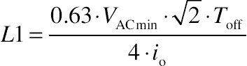
To find the inductor value at Toff min

Lmin = 60 V × 6 μs/0.2 A = 1.8 mH. Allowing for 20% tolerance, we get a value of 2.16 mH. The nearest standard value is 2.2 mH. So now we need to check Toff, using the revised inductor value of 2.2 mH.

If we let L = 2.2 mH, ipk = 200 mA and VLED = 60 V (maximum), then Toff = 7.33 μs.
But what is the Ton min period, when the AC mains voltage at its peak? If we take the peak AC mains voltage as √2 × 265 = 375 V, then the voltage across the inductor will be 375 – 60 = 315 V.

This is more than the minimum value of 700 ns, so 2.2 mH is a suitable inductor for a 60 V, 100 mA load.
Now consider an LED, such as the Osram Duris E5. This is specified at 120 mA, but would be suitable for our 100-mA load. Each LED has a maximum forward voltage drop of 2.8–3.6 V, so 16 LEDs in series would give us a load voltage of 57.6 V maximum, 51.2 V typical, or 44.8 V minimum. Consider the equations for Ton and Toff using the minimum voltage.

These results verify that a 2.2-mH inductor is quite suitable.
The advantage of using BCM is that the PF is good, but the disadvantage is high-ripple current in the LED. Capacitor C3 across the LEDs helps to maintain LED current, even when the inductor current drops to zero.
Power Integrations is another manufacturer making a buck control IC that has a reasonable PFC performance, the LYT7503D. The control technique is described as critical conduction mode, which is basically the same as BCM used by the Diodes part AL1676 described earlier in this section. Reference designs for 120 V AC operation, using the LYT7503D, suggest that the circuits produce PFs of 0.9–0.95. These designs also allow triac dimming, although the design notes suggest that there may be flickering/shimmering present and give suggestions on how to reduce these effects.
8.9. Common Mistakes With PFC Circuits
The most common mistake is to use the wrong inductor for L1.
Inductors are sized both for their magnetic saturation level and for resistive heating. Thus an inductor may be specified as iav = 500 mA, isat = 400 mA. This means that the inductor can pass 500 mA with a temperature rise of, say, 40°C. But it can only pass 400 mA before the inductance is reduced by, say, 10%. If this inductor were used in a PFC stage with a peak current of 400 mA it would overheat.
Inductor manufacturers do not normally specify magnetizing losses. The magnetic saturation levels are material dependent; the maximum flux density of ferrite is usually 200 mT, but can be higher for other materials. So when designing a ferrite-based inductor, a manufacturer will make the design based on this level. However, if the flux is changing from zero to a maximum level (such as in a PFC circuit), a significant amount of energy is lost in the ferrite core due to magnetization losses. The core loss can be considered a sort of magnetic resistance. So, a flux density limit of about 50–100 mT would be a better choice for a ferrite-based energy storage inductor in a PFC circuit, to prevent significant core heating due to these magnetization losses.
8.10. Conclusions
Detailed design analysis has not been given for the all of the PFC circuits. This chapter has been intended to show readers some options and point out limitations. For example, driving a single LED may require a BBB circuit because of the large step-down ratio, but longer strings can be driven from a Bi-Bred or a PFC stage followed by a buck converter.
Application notes from ST Microelectronics and Microchip cover the PFC, Bi-Bred, and BBB circuits in detail. These are proprietary and specialized solutions that are still evolving; interested readers should consult these application notes for the latest designs.
..................Content has been hidden....................
You can't read the all page of ebook, please click here login for view all page.