
Chapter 9
Fly-Back Converters and Isolated PFC Circuits
Abstract
This chapter discusses fly-back and isolated power factor correction circuits. Single-, double-, and triple-winding inductor/transformer types are discussed. There is some discussion about transformer design, although the detail of these is in later chapters.
Keywords
isolation
fly-back
power factor
PFC
power factor correction
transformer
A traditional fly-back converter uses an inductor with at least two windings (really, this is a transformer). Considering two windings; one is the primary, which is connected to the input power supply and a switch to ground; the other is the secondary, which is connected to the load. The circuit is arranged so that magnetic energy is stored in the inductor while switch is on; the current increases in the primary winding during this time. When the switch is off, the magnetic energy is released by current flowing out of the secondary winding. This is shown in Fig. 9.1.

Figure 9.1 Fly-Back Principle.
The energy release is the “fly-back,” so-called because in early television sets with a cathode ray tube, the fast rising voltage from a transformer winding was used to deflect the electron beam back to the starting point on the screen (the electron beam had to “fly back” quickly after completing a scan across the screen, to avoid missing the next line of data to be displayed).
Fly-back power supplies are relatively easy to design, but are more suited to constant voltage outputs. This is because the energy is stored in bursts, in a large reservoir capacitor at the output, and controlling the average voltage across the capacitor can be achieved with simple feedback. A constant current output is possible, but slightly more complex to design.
Fly-back converters are often used when the load must be isolated from the supply. Most fly-back circuits are used with AC mains input. By using constant on-time switching, they allow a good power factor (important in AC mains applications, as we saw in the last chapter). Transformer-coupled circuits are less efficient than simple buck circuits and usually more costly, but if mechanical isolation from the AC mains is impossible, they are the only choice.
Some nonisolated fly-back circuits have a common ground connection, so that feedback can be directly applied to the control IC. Driving an isolated LED load is possible if the secondary winding is completely isolated from the primary winding. Some general-purpose applications can use simple current limit techniques in the primary winding to control the output current from the secondary winding: basically controlling the power only. More accurate control will either require an optocoupler for the feedback signal, or primary side control. In primary side control, signals reflected back from the load cause modulation on the primary winding (when the primary switch is not conducting) and these signals are used for feedback.
Two semiconductor companies dominate the supply of control ICs for both isolated and nonisolated fly-back converters. One company is iWatt, now part of Dialog Semiconductor, with parts like the IW3688. The other major supplier is Power Integrations, with parts like the LYT4322E. Both of these driver ICs enable good PFC and triac phase dimmer operation, which are ideal characteristics for light bulb replacements.
9.1. Single-Winding Fly-Back (Buck–Boost)
Some fly-back converters use an inductor with a single winding. These are buck–boost controllers and are an alternative to the boost–buck converters like Ćuk and SEPIC types that were discussed in Chapter 7. Clearly, isolation is not possible with this type of converter because a single inductor winding is used for both the primary and secondary currents. This is shown in Fig. 9.2.

Figure 9.2 Buck–Boost Converter.
Current is forced through the inductor when the MOSFET switches on and connects the inductor across the power supply rail. The current level rises almost linearly with time. At a predetermined current level, the MOSFET is turned off and, since the current flow cannot stop instantly, it is forced to flow through a diode to charge the output capacitor and drive the load. The current in the inductor falls back to zero as the energy stored in the magnetic core is depleted. The single-winding fly-back can be calculated from the number of volt-seconds on the charge cycle equaling the number of volt-seconds on the discharge cycle.
The duty cycle of a buck–boost converter (continuous conduction mode) is given by the equation:

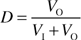
So, if we have VIN = 24 V and VOUT = 30 V, D = 30/54 = 0.555.
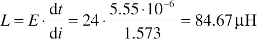
In practice we want discontinuous conduction mode because continuous conduction mode is difficult to stabilize. This means that the inductor current falls to zero at the end of each cycle. So, assume we want 350 mA output and 100 kHz switching frequency. The period is 10 μs, so the on-time is 5.55 μs and the off-time is 4.45 μs. During the off-time, the current in the inductor falls linearly from a peak level to zero. To average 350 mA output, the average inductor current during the off-time must be 350/0.445 mA = 786.5 mA, so the peak current must be double this, or 1.573 A. This also means that during the on-time, the current must rise from zero to 1.573 A.
The voltage from the power supply is 24 V, so using the familiar equation:

In practice there should be some dead time allowed, when the inductor carries no current, to ensure discontinuous conduction mode. This dead time is to allow for power supply tolerances, inductor tolerances, etc. Too much dead time means that the peak current is higher and this reduces the efficiency of the power supply.
Suppose we allow 25% tolerance, so that the on-time is 4.44 μs; this will reduce the inductance by 25%.

The off-time will be reduced unless the peak current is increased in proportion.


Increasing the peak current by 25% gives the desired result. The peak current is set by the value of current sense resistor between the MOSFET source and ground.
9.2. Two-Winding Fly-Back
A schematic of a typical fly-back circuit for driving LEDs is shown in Fig. 9.3. The dot alongside the transformer winding indicates the start of the winding. In this case the start is connected to the MOSFET drain, which alternates between a ground connection and open circuit. The voltage at the drain, and hence the winding start point, varies considerably during switching. Conversely, the outer layer (end of the winding) is at a fixed high voltage. The high voltage rail is highly coupled to ground with multiple capacitors, so that for AC signals it is effectively a ground node. Having the outer winding connected to a ground node helps to screen the inner layers, which reduces radiated EMI.

Figure 9.3 Fly-Back Circuit for LEDs.
The secondary-winding start point is connected to the output diode, which prevents conduction when the MOSFET is on. The start point of the secondary winding is connected to the anode of the output diode. Energy that is stored during the MOSFET on-time is released during the off-time, by current flowing through the output diode and into the load.
Calculation of the transformer characteristics, like inductance value and primary to secondary turns ratio, are very important in the design. In order for complete power transfer from the primary to secondary, the volt-seconds must be equal. The equation is:

9.2.1. Fly-Back Example
Let us make an isolated 3-W lamp by connecting three white power LEDs in series.
Suppose we have a primary voltage of 48 V and an on-time of 5 μs, and the primary to secondary turns ratio is 1:0.1. If we are driving a 10-V LED load, the off-time will be given by transposing the equation

Thus TOFF = 2.4 μs. Thus the switching period must be greater than 7.4 μs to allow complete removal of the magnetic energy in the transformer core. A switching frequency of below 130 kHz will be satisfactory, let us use 100 kHz to give some margin.
With 100 kHz switching, the period will be 10 μs. If the average output current is 350 mA, the average in 2.4 μs will be 1.46 A (350 mA * 10/2.4 = 1.46 A). Since this current decays linearly from the transformer winding, the peak secondary current will be double this: 2.92 A. The secondary inductance will be


Since the primary has 10 times the turns of the secondary, the primary inductance will be 100 times that of the secondary (the turns ratio, N, is squared when calculating inductance). In other words, the primary inductance will be 822 μH.
Most current-mode power supplies control the switching so that the MOSFET turns off when a certain peak current is reached in the primary winding. Since the peak current in the secondary is 2.92 A and the turns ratio is 10:1, we need a peak primary current of 292 mA. [Check: , so E = 822 * 10−6 * 0.292/(5 * 10−6) = 48 V].
, so E = 822 * 10−6 * 0.292/(5 * 10−6) = 48 V].The problem with the design that we have is that the LED current will change if the LED voltage changes because we have based our design on a certain output voltage. Actually this gives a constant power output, assuming a constant voltage input, which is fine for noncritical designs. But what if the input voltage changes?
A higher input voltage will mean that the current limit will be reached in a shorter time. This means that the duty cycle will be reduced and hence the number of volt-seconds on the primary will be unchanged. In practice, inherent delays in the current sense comparator will cause the input current to “overshoot” the reference level. This overshoot is greater with increasing input voltage because the delay is constant but the rate of current rise is increasing with input voltage. Compensation of this overshoot can be achieved by connecting resistor between the supply voltage rail and the current sense pin. This resistor injects a small DC bias that increases with increasing supply voltage and thus triggers the comparator earlier as the supply voltage rises.
The 10:1 turns ratio and 10 V output used in the previously mentioned example cause a reflected voltage of 100 V in the primary winding when the secondary conduction takes place. This reflected voltage adds to the supply voltage, so a MOSFET with a 200 V or higher voltage rating is required when powering this circuit from a 48-V supply.
The design example does not allow for efficiency. In practice a fly-back converter has about 90% efficiency, so the input current must be increased by about 10% to allow this.
If we were designing a constant voltage circuit, we would allow the peak primary current to be higher than that given in the example. This margin allows for the input voltage variations. We would then use feedback from the output to control the switching, to reduce the power in the primary, as necessary.
9.3. Three-Winding Fly-Back
Some fly-back power supplies use a third winding, called a bootstrap or auxiliary winding, as shown in Fig. 9.4. This is used to power the control IC, once the circuit is operating. The bootstrap winding has the same orientation as the secondary winding and the voltage is simply determined by the turns ratio of the bootstrap compared to the secondary. In our example of a 10-V output from the secondary, the bootstrap could have the same number of turns and thus give (approximately) 10 V for powering the control IC.

Figure 9.4 Fly-Back Using A Three-Winding Transformer.
At start-up, there is no power available from the bootstrap winding, so a start-up regulator is required. In the circuit shown in Fig. 9.4, a Microchip HV9120 is shown, which has an internal start-up regulator. However, many PWM controllers operate from low voltage and thus need an external start-up circuit. Example start-up regulators are the LR645 and the LR8 from Microchip; these give a low voltage and low current output from an input with a voltage as high as 450 V. Once the bootstrap produces power, the start-up regulator turns off. This is more efficient than using a dropper resistor and Zener diode as a start-up circuit.
9.3.1. Design Rules for a Fly-Back Converter
This section gives design rules for a fly-back converter based on either turns ratio selection determined by the maximum duty cycle allowed (Case 1), or by the optimum turns ratio based on the maximum working voltage of the MOSFET switch (Case 2). In Case 1, a design based on the maximum duty cycle (at the lowest input voltage) allows the widest input voltage range. In Case 2, a design based on the maximum voltage across the MOSFET allows a potentially lower cost solution. Alternatively, a fly-back design based on an already available transformer with a known (and fixed) turns ratio may be considered.
The transfer function of a fly-back converter is:

So the duty cycle can be found by transposing the equation:

9.3.2. Case 1: Turns Ratio Based on Maximum Duty Cycle
Given the minimum input voltage VI_MIN, output voltage VO, and maximum duty cycle DMAX, the turns ratio N can be calculated:

DMAX is typically chosen as 45% (0.45) for a PWM controller with a maximum 49% duty cycle.
If we take the earlier example of 48-V input (say, 46 V minimum), 10-V output (add 0.6 V for the output diode), and allow 45% duty cycle, we get:

This is the minimum value. A transformer with a convenient turns ratio of 1:0.33 (3:1) could be used. The maximum duty cycle will then be:

9.3.3. Case 2: Turns Ratio Based on Maximum Switch Voltage
The output voltage across the secondary winding is induced into the primary and magnified by the turns ratio N. This was illustrated at the beginning of this chapter, when a 10 V output caused 100 V to be induced into the primary winding of a 10:1 turns ratio transformer. Considering that the supply voltage was only 48 V, this forced us to use a 200-V MOSFET as the primary switch. The aim here is to minimize the MOSFET switch operating voltage requirement.
As the voltage reflected into the primary often has some ringing, a snubber circuit is used to limit the voltage across the primary winding. Ringing is due to resonance between the MOSFET drain capacitance, parasitic capacitance in the circuit, and parasitic inductance of the transformer primary. Parasitic inductance in the transformer is often referred to as “leakage inductance” because it is the proportion of the primary inductance that is not coupled into the secondary, so the magnetic field “leaks out.”
A Zener diode is sometimes used as a snubber. The voltage across the Zener diode will be greater than the voltage induced into the primary from the secondary (output) voltage, otherwise power dissipation and losses will both be very high.
To find the secondary-winding voltage, the forward voltage drop of the output diode, VF, must be added to the output voltage.

As a safety margin,  .
.
In the example we used earlier, with 48 V input, we could have used a 100-V switch and a 33-V Zener diode. The output is 10 V, so allowing for VF this becomes 10.6 V across the secondary winding:

We could use a transformer with 2:1 turns ratio (N = 0.5). The primary voltage induced from the secondary winding will be 21.2 V, which is below the Zener diode voltage by 11.8 V, which is a reasonable margin to minimize power dissipation. The peak voltage across the MOSFET drain will be limited to 48 V + 33 V = 81 V.
With a turns ratio of 2:1, the maximum duty cycle with a 46 V minimum input voltage will be:

9.3.4. Inductance Calculations
Now as we have the turns ratio (by either means described earlier) and the maximum duty cycle, we can determine the inductance and switching current. Let us use Case 1, with 41% as the maximum duty cycle.

The output power is 10 V × 0.35 A = 3.5 W and the efficiency can be guessed at as being 85%. The input power is then 4.12 W. The input current at minimum input voltage is then:


At 46 VIN and 41% duty cycle:

With 60 kHz switching, the period will be 16.667 μs. With a 41% duty cycle, the switch on-time will be 6.835 μs. So we need the primary current to rise by 439 mA in 6.835 μs.

The secondary has 1/3 the number of turns compared to the primary, so the inductance of the secondary will be 1/9, or 79.55 μH.
The other design parameter for the transformer is the size and AL factor of the ferrite core. The AL factor is defined as the number of nano-Henries inductance per turn (nH), of the winding wire. Inductance is then given by L = AL ∙ N2, where N is the number of turns. In a fly-back transformer an air gap between the two halves of the ferrite core is necessary to prevent magnetic saturation; as the air gap increases, the AL factor reduces. The flux density (B) will depend on the cross-sectional area of the core (AC), given in square meters. Suppose in this case we have some E20 cores available from Ferroxcube. For E20/10/6 cores, the core cross-sectional area is 32 mm2. So AC = 32 * 10−6 m2. The number of turns can be calculated, based on the design parameters mentioned earlier and using B = 200 mT as the maximum flux density:


Refer to core manufacturers’ specifications and chose a core with a lower AL value (larger gap) than calculated using the previous equation. A suitable core (3C90 material, 160 μm air gap) has an AL value, 250 nH. The number of turns can then be calculated as:

NPRI = 54 (rounding up to the next highest value. This quite conveniently gives the secondary turns as NSEC = 18, since it is 1/3.
9.4. Three-Winding Fly-Back PFC
An isolated fly-back is shown in Fig. 9.5 (based on a design in ST Microelectronics application note AN1060). This uses a coupled inductor, which has three windings on the same magnetic core: primary, secondary, and auxiliary. For the circuit description, we can ignore the auxiliary winding used to power the controller IC. The primary winding is on the input side and the secondary winding is on the output side. When the MOSFET turns on, current increases in the primary winding, storing magnetic energy in the magnetic core. Constant on-time switching ensures that the stored energy rises and falls as the AC mains voltage rises and falls, to give a good power factor.

Figure 9.5 Isolated Fly-Back PFC Circuit.
When the MOSFET turns off, after a fixed time, the magnetic energy is released by current flowing in the secondary winding. The secondary current charges three large capacitors, which provides a constant DC voltage for the load.
The secondary voltage can be higher or lower than the supply voltage, as the AC supply voltage rises and falls, hence the use of the term boost–buck. In this case, the output is a constant voltage of 15 V and up to 2 A current, but these levels could be changed to suit the application. For LED driving, a number of constant current buck circuits could be powered from the 15 V output.
..................Content has been hidden....................
You can't read the all page of ebook, please click here login for view all page.