
Chapter 7
Boost–Buck Converter
Abstract
This chapter describes boost–buck converters. These can either boost or buck the supply voltage, so the load voltage can be higher or lower than the supply voltage. These circuits are often used with battery-powered equipment and have the advantage of continuing to supply a constant current as the battery voltage falls below the LED load voltage. Both Ćuk and single-ended primary inductor converter topologies are described.
Keywords
boost
buck
PWM dimming
hysteretic control
Ćuk
SEPIC
A boost–buck converter allows for the load voltage to be higher or lower than the supply voltage. They are usually used in battery-powered applications because the battery voltage varies widely over time. The most common applications are automotive related: they are used in lighting applications for cars and trucks of course, but they are also used for lighting in caravans, camping, industrial and agricultural machinery (forklift trucks, tractors, diggers, forestry machines, etc.).
Two common types of boost–buck converter are Ćuk and single-ended primary inductance converter (SEPIC), which are single-switch converters. These comprise a boost converter followed by a buck converter. These will be described in this chapter. A less common type is the single inductor fly-back converter, which will be described in Chapter 9 with other fly-back circuits.
The power train of typical boost–buck circuit topology (used as an LED driver) is shown in Fig. 7.1.

Figure 7.1 Boost–Buck (Ćuk) Power Train.
The boost–buck converter has many advantages:
• The converter can both boost and buck the input voltage. Thus, it is ideal for cases where the output LED string voltage can be either above or below the input voltage during operation.
• The Ćuk converter has inductors in series with both the input and the output. Operating both stages in continuous conduction mode (CCM) will enable continuous currents in both inductors with low current ripple, which greatly reduces the filter capacitor requirements at both input and output. Continuous input current mode reduces the peak current levels and thus helps greatly in meeting conducted electromagnetic interference (EMI) standards.
• All the switching nodes in the Ćuk circuit are isolated between the two inductors. The input and output nodes are relatively quiet. This will minimize the radiated EMI from the converter. With proper layout and design, the converter can easily meet radiated EMI standards.
• One of the advantages of the boost–buck converter is the capacitive isolation. The failure of the switching transistor will short the input and not affect the output. Thus, the LEDs are protected from failure of the MOSFET.
• The two inductors L1 and L2 can be coupled together on one core. When coupled on a single core, the ripple in the inductor current from one side can be transferred completely to another side (ripple cancellation technique). This would allow, for example, the input ripple to be transferred completely to the output side making it very easy for the converter to meet conducted EMI standards. The circuit must operate in constant frequency mode in order to remain stable with coupled inductors.
Boost–buck circuits are often used in automotive applications, where the LED voltage can be higher or lower than the supply voltage. The battery voltage in a vehicle can vary considerably, depending on whether the battery is charging or discharging, the load on the system, etc. Also, the LED load voltage can change as the LEDs get warm and their forward voltage drops. By boosting first, higher voltage nodes in the circuit are then available to provide power to keep the switching regulator powered when the supply voltage dips to low levels, such as during “cold-crank” (when the motor is being started).
7.1. The Ćuk Converter
Supertex (now part of Microchip) was the first supplier to introduce a dedicated Ćuk converter control IC for LED driving. This is the HV9930, which is a hysteretic mode controller. Hysteretic mode uses the output current level to control the switching, by comparing the voltage across a current sense resistor with an internal reference voltage. Thus the switching frequency changes as the supply and load voltages change. Detailed design procedures will be described in Section 7.1.6. Even readers not using the HV9930 will find useful information within these pages.
Texas Instruments has produced the TPS92690 for Ćuk converter driving. This is intended for coupled inductors, where the input and output inductors use the same magnetic core. In order to allow this, fixed frequency switching is used. The circuit topology allows the LED anode to be connected to ground, since current sensing takes place during the off-time, when the flywheel diode is conducting. A low value resistor in series with the flywheel diode is used for this purpose.
In spite of the many advantages of the Ćuk converter, four disadvantages exist which prevent its widespread use:
• The output is inverted with respect to the input. So the cathode is negative with respect to 0 V/ground. This can cause problems in a few applications.
• The converter is difficult to stabilize. Complex compensation circuitry is often needed to make the converter operate properly. This compensation also tends to slow down the response of the converter, which inhibits the PWM dimming capability of the converter (essential for LEDs).
• An output current–controlled boost–buck converter tends to have an uncontrolled and undamped resonance due to an L–C pair (L1 and C1). The resonance of L1 and C1 leads to excessive voltages across the capacitor, which can damage the circuit.
• The input and output inductors, combined with the intermediate and output capacitors, form a series LC circuit. If an input voltage step is applied, via a switch or relay contact, damped ringing can occur with the peak current reaching several amps (I have seen 20 A peaks in a 6-W circuit). Nothing much can be done to reduce this, since the Ćuk controller and the switching MOSFET are not active at this time. Adding resistors into the circuit would help, but at the cost of power dissipation and overall efficiency.
The damping of L1 and C1 can easily be achieved by adding a damping R–C circuit across C1. However, the problem of compensating the circuit so that it is stable is more complex.
7.1.1. Operation of an HV9930 Ćuk Boost–Buck Converter
The Microchip HV9930 solves the problem of compensation and achieving a fast PWM dimming response by using hysteretic current mode control. This ensures fast response and accurate current levels. However, a simple hysteretic current mode control would not work, as the converter would not be able to start-up. To overcome this problem, the HV9930 has two hysteretic current mode controllers—one for the input current and another for the output current.
During start-up, the input hysteretic controller dominates and the converter is in input current limit mode. Once the output current has built up to the required value, the output hysteretic controller takes over. This approach will also help in limiting the input current during start-up (thus providing soft-start); also current is limited in the case of an output overload or input undervoltage condition. Three resistors (for each of the two hysteretic controllers) are required to set both the current ripple and the average current, which enables a simple controller design. Thus six resistors determine the input and output performance.
This section will detail the operation of the boost–buck converter and the design of an HV9930-based converter. The design example is specifically designed for automotive applications, but it can also be applied for any DC/DC applications. At the time of writing, there is only one other device with the same functionality as the HV9930, which is the AT9933. The AT9933 has an automotive temperature specification (up to 125°C operation), whereas the HV9930 is intended for industrial and commercial applications.
The diagram of the power train for a Ćuk boost–buck converter was shown previously, in Fig. 7.1.
In steady state, the average voltages across both L1 and L2 are zero. Thus, the voltage, Vc, across the middle capacitor C1 is equal to the sum of the input and output voltages.
Vc=Vin+Vo
When switch Q1 is turned on, the currents in both inductors start ramping up (Fig. 7.2).

Figure 7.2 Ćuk Circuit: MOSFET On.
L1diL1dt=VinL2diL2dt=Vc−Vo=Vin

When switch Q1 is turned off, the currents in both inductors start ramping down (Fig. 7.3).
Figure 7.3 Ćuk Circuit: MOSFET Off.
L1diL1dt=Vin−Vc=−VoL2diL2dt=−Vo

Assuming that the switch is ON for a duty cycle D and using the fact that, in steady state, the total volt-seconds applied across any inductor is zero, we get
Vin⋅(D)=Vo⋅(1−D)⇒VoVin=D1−D

Thus, the voltage transfer function obtained for the boost–buck converter will give buck operation for D < 0.5 and boost operation for D > 0.5. The steady state waveforms for the converter are shown in Fig. 7.4.

Figure 7.4 Ćuk Converter Steady State Waveforms.
The maximum voltage seen by Q1 and D1 is equal to the voltage across the capacitor C1.
VQ1=VD1=Vc
The standard boost–buck converter is modified, by adding three additional components, for proper operation of the HV9930 (Fig. 7.5).

Figure 7.5 Modified Ćuk Circuit.
A damping circuit Rd–Cd has been added to damp the L1–C1 pair. These additional components stabilize the circuit. Typically Cd is ten times the value of C1 and Rd is a few ohms.
An input diode (D2) has been added. This diode is necessary for PWM dimming operation (in case of automobile applications, this could be the reverse polarity protection diode). This diode helps to prevent capacitors C1 and Cd from discharging when the gate signals for Q1 are turned off. Thus, when the HV9930 is enabled, the steady-state output current level will be reached quickly.
7.1.2. Hysteretic Control of the Ćuk Converter
Hysteretic control keeps the current in inductor L2 (iL2 ) between preset upper and lower boundaries. As previously shown in Fig. 7.4, the inductor current ramps up at a rate of Vin/L2 when the switch is ON and ramps down at a rate of –Vo/L2 when the switch is OFF. Thus, the hysteretic control scheme turns the switch OFF when the inductor current reaches the upper limit and turns the switch ON when it reaches the lower limit.
The average current in inductor L2 is then set at the average of the upper and lower thresholds. The ON and OFF times (and thus the switching frequency) vary as the input and output voltages change to maintain the inductor current levels. However, in any practical implementation of hysteretic control, there will be comparator delays involved. The switch will not turn ON and OFF at the instant the inductor current hits the limits, but after a small delay time, as illustrated in Fig. 7.6.

Figure 7.6 Current in the Output Inductor L2.
7.1.3. The Effects of Delay in Hysteretic Control
This delay time introduces two unwanted effects:
• It alters the average output current value. For example, if the delay on the downslope of the inductor current is more than the delay on the upslope, then the average current value decreases.
• It decreases the switching frequency, because the turn-on period and the turn-off period are both extended by the delays, which may make it more difficult for the circuit to meet EMI regulations.
These effects will have to be taken into consideration when choosing the output inductor value and setting the current limits.
Assume a peak-to-peak current ripple setting of ∆io (using the programming resistors) and a desired average current Io. A hysteretic current-controlled boost–buck converter acts as a constant-off-time converter as long as the output voltage is fixed, and the off-time is theoretically independent of the input voltage. Thus, the converter is designed assuming a constant off time Toff (the method to determine the off-time will be discussed later in the application note).
For the HV9930, as long as the switching frequencies are less than 150 kHz, these delay times have a negligible effect and can be ignored. In these cases, the output inductor can be determined by
L2=Vo⋅Toff∆io

If the inductor chosen is significantly different from the computed value, the actual off-time Toff,ac can be recomputed using the same equation.
However, in automotive applications, there is an advantage in setting the switching frequency of the converter below 150 kHz or in the range between 300 and 530 kHz. This will place the fundamental frequency of the conducted and radiated EMI outside of the restricted bands making it easier for the converter to pass automotive EMI regulations. In cases where the switching frequency is more than 300 kHz, the delay times cannot be neglected and have to be accounted for in the calculations. Fig. 7.7 illustrates the output inductor current waveform and the various rise and fall times.

Figure 7.7 Hysteretic Control With Comparator Delays.
From Fig. 7.7,
Toff=Tf1+Tf2+Tf =VinVo⋅Tr+Tf2+Tf

The desired output current ripple ∆io and the downslope of the inductor current m2 determine Tf2. The delay times of the HV9930 determine Tr and Tf. For the HV9930, the delay time of the comparators is related to the overdrive voltage (voltage difference between the two input terminals of the current sense comparator) applied as
Tdelay≈K3√m⋅(0.1/∆io)

where “m” is the rising or falling slope of the inductor current.
Tr=6 μ3√Vin⋅0.1∆io⋅3√L2=K1⋅3√L2

Tf2=∆io⋅L2Vo=K2⋅L2
Tf=6 μ3√Vo⋅0.1∆io⋅3√L2=K3⋅3√L2

To find the value of L2 using the previously mentioned time delay equations results in a cubic equation. This cubic has one real root and two complex roots. The inductor value is the real root of the cubic raised to the third power.
a=K2b=VinVo⋅K1+K3c=Toff
∆=12⋅√3⋅√4⋅b3+27⋅a⋅c2a

L2={16⋅a[(108⋅c+∆)⋅a2]1/3−2⋅b[(108⋅c+∆)⋅a2]1/3}3

The actual off-time Toff,ac can be computed by substituting the chosen inductor value back into the equations for Tr, Tf, and Tf2, to get Tr,ac, Tf,ac, and Tf2,ac.
Toff,ac=Tf1,ac+Tf2,ac+Tf,ac =VinVo⋅Tr,ac+Tf2,ac+Tf,ac

The actual ripple in the inductor current ∆io,ac is
is
∆io,ac=Vo⋅Toff,acL2

7.1.4. Stability of the Ćuk Converter
The single-switch Ćuk converter can be considered as separate boost and buck converters (in that order), which are cascaded, and both switches being driven with the same signal (Fig. 7.8).
Figure 7.8 Ćuk Converter.
The relationships between the voltages in the system are
VcVin=11−D (boost converter)VoVc=D (buck converter)

The capacitor voltage Vc and the input–output relationship can both be derived using the previous equations
VoVin=VoVc⋅VcVin=D1−D

Vc=Vin1−D=Vin1−(Vo/Vc) ⇒Vc=Vo+Vin

For the purposes of designing the damping network, it is easier to visualize the converter in its two-switch format of Fig. 7.7 rather than as the single-switch Ćuk converter. Hence, for the remainder of this section, the cascaded converter will be used to derive the equations.
In hysteretic control of the Ćuk converter using the HV9930, once the start-up phase is complete, the output buck stage is controlled and the input boost stage is uncontrolled. An equivalent schematic of the HV9930-controlled Ćuk converter is shown in Fig. 7.9.

Figure 7.9 Ćuk Controller.
The hysteretic control of the buck stage ensures that the output current iL2 is constant under all input transient conditions. So, for the purposes of average modeling, the load seen by the capacitor C1 can be modeled as a current source equal to d⋅Io , where d is the instantaneous duty cycle and Io is the constant output current. The CCM buck stage also imposes one more constraint:
Vo=d⋅vc
where d and vc are the time-dependent duty cycle and capacitor voltage and Vo is the constant output voltage. For the system to be stable, it is necessary that the control system will act to reduce any disturbance in capacitor voltage.
The loop gain of the system for a boost–buck converter without damping has a negative phase margin (i.e., the phase is less than −180° when the magnitude crosses 0 dB). This is due to the undamped LC pole pair and causes the system to be unstable. Thus, any disturbance to the capacitor voltage will get amplified and keep increasing till the components breakdown.
The addition of R–C damping of this undamped pole pair can stabilize the system and make sure that the disturbance input is properly damped. Also, the presence of Cd ensures that Rd will not see the DC component of the voltage Vc across it, reducing the power dissipated in the damping resistor (Cd blocks the DC component of the voltage).
Assuming Cd>>C1 , the loop gain transfer function of the R–C-damped boost–buck converter can be derived as
G(s)H(s)=D1−D⋅(1+s⋅Rd⋅Cd)⋅(1−s⋅D(1−D)2⋅L1⋅IoVo)(1+s⋅Rd⋅C1)⋅(1+s⋅Rd⋅Cd+s2⋅L1⋅Cd(1−D)2)

Thus, the loop has a DC gain of D/(1 − D) and includes:
1. Damping (and ESR) zero at ωz=1Rd⋅Cd ;
;
;2. RHP zero at ωRHP=(1−D)2D⋅VoL1⋅Io ;
;
;3. Complex double pole with natural resonant frequency ωo=1−D√L1⋅Cd and damping factor δ=(1−D)⋅Rd⋅√CdL1
 ;
;
and damping factor δ=(1−D)⋅Rd⋅√CdL1;4. High-frequency pole at ωp=1Rd⋅C1 .
.
.In order to achieve stable loop, the 0 dB crossing (ωc) must be placed such that ωc<<ωRHP and ωc<<ωp
 . The latter condition is easily met by selecting Cd>>C1.
We can easily obtain approximate values of Cd and Rd for the case of ωc>>ωo . This condition is usually met for the worst-case calculations at minimum input voltage, since the DC gain is the highest at this condition. Set ωc=ωRHP/N
 , where N >> 1. Then ωo can be approximately calculated from
ωo=ωc⋅√1−DD=ωRHPN⋅√1−DD

Substituting for ωo and ωRHP into the above gives the equation for computing Cd:
Cd=N2⋅D3(1−D)3L1⋅I2oV2o.

Selecting Rd such that ωz = ωc results in a good phase margin with minimum power dissipation. Then, using equations for ωz and ωRHP gives a solution for Rd:
Rd=N⋅D(1−D)2L1⋅IoCd⋅Vo.

Using the previous equations, the approximate values for the damping network can be computed using the following equations:
Cd=9⋅(D1−D)3⋅L1⋅(IoVo)2

Rd=3⋅D(1−D)2⋅L1⋅IoCd⋅Vo

Note that the damping resistor value includes the ESR or the damping capacitor. In many cases, the damping capacitor is chosen to be an electrolytic capacitor, which will have a significant ESR. In such cases, the damping resistor can be reduced accordingly.
7.1.5. Dimming Ratio Using PWM Dimming
The linearity in the dimming ratio achievable with the Boost–Buck depends on both the switching frequency and the PWM dimming frequency.
For a converter designed to operate at a minimum switching frequency of 300 kHz, one switching time period equals 3.33 μs. This is the minimum on-time of the PWM dimming cycle. At a PWM dimming frequency of 200 Hz (5-ms period), 3.33 μs equals a minimum duty cycle of 0.067%. This corresponds to a 1:1500 dimming range. However, the same converter being PWM dimmed at 1 kHz (1-ms time period) will have a minimum duty ratio of 0.33% or a PWM dimming range of 1:300.
If the minimum on-time of the PWM dimming cycle is less than the switching time period, the LED current will not reach its final value. Hence the average current will be less. Thus, the LEDs will dim, but there will be a loss of linearity between the average LED current and the duty cycle of the PWM input.
7.1.6. Design of the Ćuk Converter With HV9930
7.1.6.1. Specification
Input voltage: 9–16 V (13.5 V typical)
Transient voltage: 42 V (clamped load dump rating)
Reverse polarity protection: 14 V
Output voltage: 28 V maximum
Output current: 350 mA
LED resistance: 5.6 Ω
Estimated efficiencies: 72% minimum, 82% maximum (80% typical)
These efficiency values do not take into account the power loss in the reverse blocking diode. The diode will drop about Vd=0.5 V across it and thus will dissipate power in the range of 0.4–0.6 W. This diode voltage drop will be taken in account while designing the converter.
The efficiency values used in this design are typical values for the given input voltages and output power level. Higher efficiencies can be obtained at lower input current levels (i.e., higher input voltages): the efficiency drop at lower input voltages is due to conduction losses caused by the correspondingly larger input currents. The efficiency values will depend on the operating conditions and, except in very high power designs, these values can be used as a good approximation.
Efficiencies higher than 85% can easily be achieved with the HV9930-controlled Ćuk converter if the operating frequency is kept below 150 kHz. However because of automotive EMI requirements, the higher efficiencies are traded-off for higher switching frequencies (which increase switching losses in the system).
Consider a Ćuk converter circuit as shown in Fig. 7.10.

Figure 7.10 Ćuk Converter Using HV9930.
7.1.6.2. Switching frequency at minimum input voltage
Although the HV9930 is a variable frequency IC, the selection of the minimum switching frequency is important. In the case of automotive converters, designing with a switching frequency in the range between 300 and 530 kHz would avoid the main radio broadcast bands and make it easier to meet the conducted and radiated EMI specifications. So, for this application we choose a minimum switching frequency of 300 kHz (which occurs at minimum input voltage).
7.1.6.3. Calculating the duty cycle
The switch duty cycle will have to be computed at the minimum input voltage.
Dmax=11+ηmin⋅(Vin,min−Vd)Vo =0.821

7.1.6.4. Calculating the input current
The input current level at the minimum input voltage should be calculated first because this gives the highest current level. The value obtained will be used to work out the current ratings of the various components.
Iin,max=Vo⋅Ioηmin⋅(Vin,min−Vd) =1.601 A

7.1.6.5. Calculating the output inductor
The first step is to compute the off-time. The off-time of the converter can be calculated as
Toff=1−Dmaxfs,min =598 ns

Assuming a 25% peak-to-peak ripple in the output current (∆io=87.5 mA) , and accounting for the diode drop in the input voltage by substituting Vin,min–Vd in place of Vin, yields
598 ns=0.887 μ⋅3√L2+3.125 m⋅L2+1.89 μ⋅3√L2
Solving for L2 gives
L2=(0.052)3=145 μH
The closest standard value inductor is a 150 μH, 0.35 A RMS, and 0.4 A sat inductor.
Since the inductance value is different from the computed value, the actual off-time will also change as
Toff,ac=2.777 μ⋅3√L2,ac+3.125 m⋅L2,ac =616 ns

The actual ripple in the output current is given by
∆io,ac=Vo⋅Toff,acL2,ac =0.115 A

Note that although the ripple in the output current was assumed to be about 25% (or 87.5 mA), the actual ripple is almost double that value. This increase in the ripple is due to the delays of the comparators. A capacitor will be required at the output of the converter (across the LEDs) to reduce the ripple to the desired level. This capacitor will be very small, as the switching frequencies are large, but the capacitor will also help to reduce output EMI.
It is also useful to calculate the ripple overshoot and undershoot beyond the programmed limits. This will help determine how the average current changes due to the delays.
∆iover=VoL2,ac⋅(Vin,min−VdVo⋅K1)⋅3√L2,ac =8.3 mA

∆iunder=VoL2,ac⋅K3⋅3√L2,ac =19 mA

Thus, the average output current will be reduced from the set value by about 10.7 mA.
In most cases, due to the inductor values available, the actual off-time will differ from the computed value significantly. Thus, it is better to use the actual value of the off-time calculated in order to work out the rest of the component values.
If the switching frequency is less than 150 kHz, the equation L2=Vo⋅Toff∆io can be used to calculate the output inductance (L2) value, simplifying the procedure greatly.
can be used to calculate the output inductance (L2) value, simplifying the procedure greatly.7.1.6.6. Calculating the input inductor
We can assume a 15% peak-to-peak ripple in the input current at minimum input voltage (this low input ripple will minimize the input filtering capacitance needed). The off-time previously calculated can be used to find the value of the input inductor.
L1=Vo⋅Toff,ac0.15⋅Iin,max =72 μH

The closest standard value inductor is an 82 μH inductor. The current rating of this inductor will be decided in the final stages after the input current limit has been set.
The peak-to-peak ripple in the input current is
∆Iin=Vo⋅Toff,acL1,ac =0.21 A

7.1.6.7. Calculating the value of the middle capacitor (C1)
Assuming a 5% ripple across the capacitor at minimum input voltage (∆vc=0.1⋅(Vin,min−Vd+Vo)=1.825 V) , capacitor C1 can be calculated as
C1=Iin,max⋅Toff,ac∆vc =0.54 μF

Irms,C1=√I2in,max⋅(1−Dmax)+I2o⋅Dmax =0.72 A

The voltage rating and type of this capacitor have to be chosen carefully. This capacitor carries both the input current and the output current. Thus, to prevent excessive losses and overheating of the capacitor, it must have a very low ESR. Ceramic capacitors are an ideal choice for this application due to their low ESR and high transient voltage limit. If a ceramic capacitor cannot be used for reasons of cost or availability, a plastic film capacitor, such as PET can be used instead.
The maximum steady state voltage across the capacitor is 44 V (= 28 V + 16 V), and the maximum transient voltage across the capacitor Vc,max is 70 V (= 28 V + 42V). Ceramic capacitors can easily withstand up to 2.5 times their voltage rating for the duration of the load dump voltage. Also, the actual capacitance value of these capacitors reduces based on the bias voltage applied. Ceramic capacitor types X7R and X5R are more stable and the capacitance drop is not more than 20% at full rated voltage.
Thus, a 0.47 μF, 50 V X7R ceramic chip capacitor can be selected.
7.1.6.8. Choosing the switching transistor (Q1)
The peak voltage across the MOSFET Q1 is 70 V. Assuming a 30% overhead on the voltage rating to account for leakage inductance spikes, the MOSFET voltage needs to be at least
VFET=1.3⋅Vc,max =91 V

The RMS current through the MOSFET will be at maximum level at low input voltage (higher current levels and maximum duty cycle). The maximum RMS current through the MOSFET is
IFET,max=(Iin,max+Io)⋅√Dmax =1.77 A

A typical choice for the MOSFET is to pick one whose current rating is about 3 times the maximum RMS current. Choose FDS3692 from Fairchild Semiconductors (100 V, 4.5 A, 50 mΩ N-channel MOSFET). Note that the current rating is normally quoted at 25°C.
The total gate charge Qg of the chosen MOSFET is a maximum of 15 nC. It is recommended that the MOSFET total gate charge should not exceed 20 nC, as the large switching times will cause increased switching losses. A higher gate charge would be allowable if the switching frequency can be reduced appropriately.
7.1.6.9. Choosing the switching diode
The maximum voltage rating of the diode D2 is the same as the MOSFET voltage rating. The average current through the diode is equal to the output current.
Idiode=Io=350 mA
Although the average current of the diode is only 350 mA, the actual switching current through the diode goes as high as 1.95 A (Iin,max + Io). (Note: the calculations were for 360 mA, to allow for 10 mA drop because of delays, but the actual average current is 350 mA.) A 500-mA diode will be able to carry the 1.79 A current safely, but the voltage drop at such high current levels would be extremely large increasing the power dissipation. Thus, we need to choose a diode whose current rating is at least 1 A. A 100 V, 2 A Schottky diode would be a good choice.
7.1.6.10. Choosing the input diode
The input diode serves two purposes:
1. It protects the circuit from a reverse polarity connection at the input.
2. It helps in PWM dimming of the circuit by preventing C1 from discharging when the HV9930 is turned off.
The current rating of the device should be at least equal to Iin,max. The voltage rating of the device should be more than the reverse input voltage rating. A higher current rating often gives a lower forward voltage drop. In this case, a 30BQ015 (15 V, 3 A Schottky diode) would be a good choice.
7.1.6.11. Calculating the input capacitance
Some capacitance is required on the input side to filter the input current. This capacitance is mainly responsible for reducing the second harmonic of the input current ripple (which in this case falls in the AM radio band). According to the SAE J1113 specifications, the peak limit for narrowband emissions in this range is 50 dBμV to meet Class 3 at an input voltage of 13 ± 0.5 V. Assuming a sawtooth waveform for the input current as a conservative approximation, the RMS value of the second harmonic component of the input current (Iin,2) can be computed as
Iin,2=∆Iin2⋅√2⋅π=0.024 A

The switching frequency of the converter at 13 V input can be computed as
Dnom=11+ηnom⋅(Vin,nom−Vd)Vo =11+0.8⋅(13.5−0.5)28 =0.73

fs,nom=1−DnomToff,ac =414 kHz

Cin=Iin,24⋅π⋅fs,nom⋅10−6⋅1050/20 =14.6 μF

Choose a parallel combination of three 4.7 μF, 25 V, X7R ceramic capacitors.
7.1.6.12. Calculating the output capacitance
The output capacitance is required to reduce the LED current ripple from 115 mA to ∆ILED = 70mA (20% peak-to-peak ripple) can be approximately calculated by using only the first harmonic in the inductor current. A 70 mA peak-to-peak ripple in the LED results in a 392 mV (∆vo=∆ILED⋅RLED) peak-to-peak ripple voltage. Then
∆vo2=8π2⋅(∆iL22)⋅RLED√1+(2⋅π⋅fs,min⋅RLED⋅Co)2

The output capacitance required can then be calculated from this as
Co=√(16⋅RLEDπ2⋅∆iL2∆vo)2−12⋅π⋅fs,min⋅RLED =0.178 μF

Use a 0.22 μF, 35 V ceramic capacitor.
7.1.6.13. Calculating the theoretical switching frequency variation
The maximum and minimum frequencies (using steady state voltage conditions) can be now be worked out:
fs,min=1−11+ηmin⋅(Vin,min−Vd)/VoToff,ac =291 kHz

fs,max=1−11+ηmax⋅(Vin,max−Vd)/VoToff,ac =506 kHz

The theoretical frequency variation for this design is 398 kHz ± 27%.
7.1.6.14. Design of the damping circuit
The values for the damping network can be calculated as follows
Cd=9⋅(Dmax1−Dmax)3⋅L1,ac⋅(IoVo)2 =11 μF

Rd=3⋅Dmax(1−Dmax)2⋅L1,ac⋅IoCd⋅Vo =7.16 Ω

The power dissipated in Rd can be computed as
PRd=∆v2c12⋅Rd =3.65212⋅7.16=0.155 W

The RMS current through the damping capacitor will be
iCd=∆vc2⋅√3⋅Rd=0.147 A
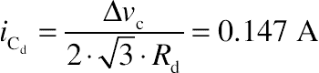
Choose a 10 μF, 50 V electrolytic capacitor that can allow at least 150 mA RMS current. An example would be EEVFK1H100P from Panasonic (10 μF, 50 V, Size D). This capacitor has about a 1 Ω ESR, so Rd can be reduced to about 6.2 Ω.
7.1.6.15. Internal voltage regulator of the HV9930
The HV9930 includes a built-in 8–200 V linear regulator. This regulator supplies the power to the IC. This regulator can be connected at either one of two nodes on the circuit as shown in Fig. 7.11.

Figure 7.11 Connection Points for Vin.
(A) HV9930 powered directly from supply. (B) Powered via switching node.
(A) HV9930 powered directly from supply. (B) Powered via switching node.
In the normal case, when the input voltage is always greater than 8 V, the Vin pin of the IC can be connected to the cathode of the input protection diode (as shown in Fig. 7.11A). If reverse protection is not provided, the Vin pin can be connected directly to the positive supply.
In conditions where the converter needs to operate at voltages lower than 8 V, once the converter is running (as in the case of cold-crank operation), the VIN pin of the HV9930 can be connected as shown in Fig. 7.11B. In this case, the drain of the MOSFET is at Vin + Vo, and hence even if the input voltage drops below 8 V, the IC will still be functioning. However, in this case, more hold-up capacitance will be required at the VDD pin to supply the power to the IC when the MOSFET is ON.
In both cases, a 2.2 μF or greater value ceramic capacitor is recommended at the VDD pin.
7.1.6.16. Internal voltage reference
The HV9930 includes an internal 1.25 V (±3%) reference. This reference can be used to set the current thresholds for the input and output hysteretic comparators. It is recommended that this pin be bypassed with at least a 0.1 μF ceramic capacitor, in order to keep the impedance low and reduce noise.
7.1.6.17. Programming the hysteretic controllers and overvoltage protection
The input and output current levels for the hysteretic controllers are set by means of three resistors for each current—one current sense resistor and two divider resistors. The equations governing the resistors are the same for both the input and output sides and are given as
RsRref=0.05⋅∆iI+0.11.2⋅∆iI−0.1

Rcs=1.2⋅RsRref−0.05I

These equations assume that the 1.25 V reference provided by the HV9930 is used to set the current. In cases where linear dimming of the LEDs is required, it is recommended that the input current thresholds be based on the 1.25 V reference and the output current thresholds are modified using the variable input voltage available. In such a case, assuming the maximum external voltage VLD as the reference, the previous two equations can be modified as
RsRref=0.05⋅∆iI+0.1(VLD−0.05)⋅∆iI−0.1

Rcs=(VLD−0.05)⋅RsRref−0.05I

In this design example, it is assumed that linear dimming is not required and the 1.25 V reference is used for both the input and output programming.
Note: The HV9930 cannot operate the boost–buck converter in the discontinuous conduction mode, so there is a minimum external voltage reference that can be used. The minimum external voltage is given by
VLD=0.1⋅Rref2+Rs2Rs2,

The programming of the output side is also linked to the overvoltage protection. The boost–buck converter is not inherently programmed against open LED conditions, so external protection is required. This is achieved by adding Zener diode D3, and by splitting the resistor Rs2 into two parts—Rs2a and Rs2b. In normal operation, the inductor current will flow only through Rcs2 and the voltage drop across Rcs2 is sensed through Rs2a and Rs2b in series.
When there is an open LED condition, the inductor current will flow through diode D3. This will then clamp the output to the Zener breakdown voltage. However, since the diode cannot take the full design current, the current level has to be reduced to more manageable levels. During open LED conditions, the current will flow though both Rcs2 and Rs2a. Thus, the effective current sense resistor seen by the IC is Rcs2 + Rs2a and the voltage drop across both of these will be sensed through Rs2b. This provides a feedback signal to the output comparator to reduce the programmed current level and thus prevent the high LED currents from flowing into the Zener diode.
7.1.6.18. Choosing the output side resistors
For the output current, Io = 0.36A (to compensate for the 10 mA drop due to the delay times) and ∆Io = 87.5 mA. Note that we are using the values assumed and not the actual values computed in Section 7.1.6.5 for the ripple current. Using these values in the previous equations,
Rs2a+Rs2bRref2=0.534
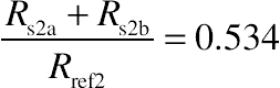
Rcs2=1.64 ΩPRcs2=0.352⋅1.64=0.2 W

Before we complete the design of the output side, we also have to design the overvoltage protection. For this application, choose a 33-V Zener diode. This is the voltage at which the output will clamp in case of an open LED condition. For a 350-mW diode, the maximum current rating at 33 V works out to be about 10 mA. Using a 5 mA current level during open LED conditions, and assuming the same Rs / Rref ratio,
Rs2a+Rcs2=120 Ω.
Choose the following values for the resistors:
Rcs2=1.65 Ω,1/4 W,1%Rref2=10 kΩ,1/8 W,1%Rs2a=100 Ω,1/8 W,1%Rs2b=5.23 kΩ,1/8 W,1%

7.1.6.19. Design of the input side resistors
For the input side, we first have to determine the input current level for limiting. This current level is dictated by the fact that the input comparator must not interfere with the operation of the circuit, even at minimum input voltage.
The peak of the input current at minimum input voltage will be
Iin,pk=Iin,max+∆Iin2 =1.706 A

Assuming a 30% peak-to-peak ripple when the converter is in input current limit mode, the minimum value of the input current will be
Ilim,min=0.85⋅Iin,lim
We need to ensure that Ilim,min>Iin,pk for proper operation of the circuit. Assuming a 5% safety factor, that is,
Ilim,min=1.05⋅Iin,pk,
we can compute the input current limit to be Iin,min = 2.1A.
Allowing for a 30% peak-to-peak ripple, we can calculate
Rs1Rref1=0.442

Rcs1=0.228 ΩPRcs1=I2in,lim⋅Rcs1=1 W

This power dissipation is a maximum value, which occurs only at minimum input voltage. At a nominal input voltage of 13.5 V, we can compute the input current using the nominal values for the efficiency and the input voltage.
Iin,nom=28⋅0.350.8⋅(13.5−0.5) =0.942 A

PRcs1=0.9422⋅0.228=0.2 W
Thus, at nominal input voltage, the power dissipation reduces by about 5 times to a reasonable 0.2 W.
Choose the following values for the resistors:
Rcs1=Parallel combination of three 0.68 Ω, 1/2 W, 5% resistors
Rref1=10 kΩ,1/8 W,1%Rs1=4.42 kΩ,1/8 W,1%

7.1.6.20. Input inductor current rating
The maximum current through the input inductor is Ilim,max=1.15⋅Iin,lim=2.4 A . Thus, the saturation current rating of the inductor has to be at least 2.5 A. If the converter is going to be in input current limit for extended periods of time, the RMS current rating needs to be 2 A, else a 1.5 A RMS current rating will be adequate.
7.1.6.21. Improving efficiency
The input current sense resistor can be reduced in value, which gives reduced power dissipation (loss). To allow this, it is necessary to add an extra resistor (RA) between the anode of the flywheel diode and the current sense input of the HV9930 (AT9933). This resistor allows a reduction in the hysteresis required by the input comparator. The additional resistor is shown in Fig. 7.12.

Figure 7.12 Modification of the Ćuk Circuit.
Consider the circuit during the period when the MOSFET is ON, so that the input current through L1 is increasing by ∆Iin/2, until it reaches Iin,lim + ∆Iin/2. With the MOSFET turned ON, the positive side of the capacitor C1 is grounded and the other side of C1, which is connected to resistor RA, is at potential −VC1. Note that the potential −VC1,nom = Vin,nom + Vo. The voltage reference for the comparator input at CS1 is 0 V. Now consider the node at CS1 in terms of current flow; CS1 is high impedance input, so the sum of currents equal zero:
VrefR7=VC1,nomRA+(Iin,lim+∆Iin2)⋅R1‖

Now consider the circuit when the MOSFET is OFF. Now the flywheel diode D3 is conducting, so the negative side of capacitor C1 is grounded (the small forward voltage of the diode can be ignored). With the MOSFET turned OFF, the voltage reference for the comparator input at CS1 is 100 mV.

Since RA is a very large value and the voltage across it is small, we can ignore its effect to simplify the calculations:

We can thus ignore the addition of RA during the period that the MOSFET is turned OFF. Clearly, the value of R1‖ R3 can be reduced if the current  can be increased, or if R4 can be decreased, or both.
can be increased, or if R4 can be decreased, or both.The maximum current sense voltage occurs when the MOSFET is first turned ON.

This is a function of the voltage across the capacitor C1. If we take another look at the equation for current flow when the MOSFET is turned ON:
In a Ćuk topology, VC1 = Vin + Vout. At start-up, Vout = 0 V, so VC1,min = Vin,min. The highest input current occurs at Vin,min.

If we set the maximum current  in the modified circuit to be equal to the inductor L1 saturation current, Isat, we get
in the modified circuit to be equal to the inductor L1 saturation current, Isat, we get

In practice we start with the design of an unmodified circuit, so are the values calculated before the addition of RA is considered. In the modified circuit, Isat (of L1) must be much higher than these values to gain the loss reduction benefit, which gives a higher input ripple at start-up.
are the values calculated before the addition of RA is considered. In the modified circuit, Isat (of L1) must be much higher than these values to gain the loss reduction benefit, which gives a higher input ripple at start-up.
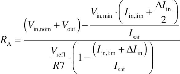


Vref1 = 1.25 V in the standard configuration.
Let us see the effect of allowing 30% input current ripple.

The input current sense resistor, Rcs1, is reduced from 0.228 to 0.09 Ω, which reduces the conduction losses in the circuit to less than half the original value.
7.1.6.22. Meeting conducted and radiated EMI
Due to the nature of the Ćuk boost–buck converter, it is easy to meet conducted and radiated EMI specifications. A few precautions need to be taken during design and PCB layout to be able to meet the EMI standards.
1. In some cases, when the input current ripple is too large or the switching frequency of the converter is above 150 kHz, it might not be possible to meet the conducted EMI standards using only capacitors at the input. In such cases, an input PI filter might be required to filter the low frequency harmonics.
2. Shielded inductors or toroidal inductors should always be preferred over unshielded inductors. These inductors will minimize radiated magnetic fields.
3. During layout, the IC and MOSFET ground connection should be connected to a copper plane on one of the PCB layers with the copper plane extending under the inductors.
4. The loop consisting of Q1, C1, and D1 should be as small as possible. This would help greatly in meeting the high frequency EMI specifications.
5. The length of the trace from GATE output of the HV9930 to the GATE of the MOSFET should be as small as possible, with the source of the MOSFET and the GND of the HV9930 being connected to the GND plane. A low value resistor (10–33 Ω) in series with GATE connection will slow down the switching edges and greatly reduce EMI, although this will cause efficiency to decrease slightly.
6. An R–C damping network might be necessary across diode D1 to reduce ringing due to the undamped junction capacitance of the diode. Such a circuit is often called a “snubber.”
This concludes the Ćuk converter design. We can now consider a closely related circuit; the SEPIC.
7.2. SEPIC Boost–Buck Converters
The abbreviation SEPIC comes from the description—single-ended primary inductance converter. A SEPIC is a boost–buck converter, like a Ćuk, so its input voltage range can overlap the output voltage. SEPIC circuits can be designed for constant voltage or constant current output.
The SEPIC topology has been known for some time, but only recently has there been a revival in its application because: (1) it needs low-ESR capacitors and these are now widely available and (2) it can be used to create AC input power supplies with power factor correction (PFC) that are used to meet worldwide EMI standards.
In automotive and portable applications, batteries are used as a power source for DC–DC converters. A 12 V supply used in automotive applications can have a wide range of terminal voltage, typically 9–16 V during normal operation using a lead-acid battery, but can go as low as 6.5 V during cold-crank and as high as 90 V during load-dump (when the battery is disconnected). The peak voltage is usually clamped to about 40 V, using a voltage-dependent resistor to absorb the energy.
Lithium batteries have been very successful in portable applications, thanks mostly to their impressive energy density. A single lithium cell provides an open voltage of 4.2 V when fully charged, and replaces up to three of the alternative NiCd or NiMH cells. During discharge the cell still retains some energy down to 2.7 V. This input voltage range can be both above and below the output voltage of many DC/DC converters and so discounts the possibility of using simple boost or buck converters.
International standards for AC mains power supplies rated above 75 W require PFC. Having a good power factor means that the current waveform from the AC line is sinusoidal and in phase with the voltage. A power factor of 1 is perfect and is only achieved with a resistive load. Most PFC circuits use a simple step-up converter as the input stage, implying that the input stage output must exceed the peak value of the input waveform. In Europe AC inputs of 190–265 V RMS are found, which impose an output of at least 375 V, forcing the following converters to work with elevated input voltages. Typically a PFC input stage has a 400 V output.
By using a SEPIC topology, which has a boost–buck topology, the boost section provides PFC and the buck section produces a lower output voltage. This provides a compact and efficient design. It provides the required output level even if the peak input voltage is higher. More detail on PFC circuits will be given in Chapter 8.
7.2.1. Basic SEPIC Equations
The boost or step-up topology, as shown in Fig. 7.13, is the basis for the SEPIC converter. The boost converter principle is well understood: first, switch Q1 conducts during the on-period, Ton, which increases the current in L1 and thus increases the magnetic energy stored there. Second, the switch stops conducting during the off-period, Toff, but the current through L1 cannot change abruptly—it continues to flow, but now through diode D1 and into Cout. The current through L1 decreases slowly as the stored magnetic energy decreases. Capacitor Cout filters the current pulse that was generated by L1 when Q1 turned off.

Figure 7.13 The Boost Converter Topology Which is the Basis for SEPIC Power Supply Circuits.
The diode D1 has to switch very quickly, so a diode with a short reverse recovery time (Trr less than 75 ns) is needed. In cases where Vout is relatively low, the efficiency can be improved by using a Schottky diode with low forward voltage (about 400 mV) for D1.
Note that a boost converter has one major limitation: Vout must always be higher than Vin. If Vin is ever allowed to become greater than Vout, D1 will be forward biased and nothing can prevent current flow from Vin to Vout.
The SEPIC scheme in Fig. 7.14 removes this limitation by inserting a capacitor (Cp) between L1 and D1. This capacitor blocks any DC component between the input and output. The anode of D1, however, must connect to a known potential. This is accomplished by connecting D1 to ground through a second inductor (L2). L2 can be separate from L1 or wound on the same core, depending on the needs of the application.

Figure 7.14 SEPIC Topology.
If L1 and L2 are wound on the same core, which is simply a transformer, one might argue that a classical fly-back topology is more appropriate. However, the transformer leakage inductance, which is not a problem in SEPIC schemes, often requires a snubber network in fly-back schemes. Snubber networks are described later in this chapter; put simply they require additional components that must be carefully selected to minimize losses.
Parasitic resistances that cause most of the conduction losses in a SEPIC are RL1, RL2, Rsw, and  which are associated with L1, L2, SW, and Cp, respectively. These parasitic components are also shown in Fig. 7.14.
An advantage of the SEPIC circuit, besides buck and boost capability, is a capacitor (Cp) that prevents unwanted current flow from Vin to Vout. Thus the limitation of the simple boost converter, that Vin had to always be less than Vout, has been overcome.
Though it has very few elements, the operation of a SEPIC converter is not so simple to describe by equations; some assumptions have to be made. First, assume that the values of current and voltage ripple are small with respect to the DC components. Second, assume that at equilibrium there is no DC voltage across the two inductances L1 and L2 (neglecting the voltage drop across their parasitic resistances). By using these assumptions, Cp sees a DC potential of Vin at one side (through L1) and ground on the other side (through L2). The DC voltage across Cp is:
The period of one switching cycle is T = 1/frequency. The portion of T for which switch Q1 is closed is the duty cycle, D, and the remaining part of the period is thus 1 − D. As the mean voltage across L1 equals zero during steady-state conditions, the voltage seen by L1 during D * T (i.e., the MOSFET “ON” period) is exactly compensated by the voltage seen by L1 during (1 − D) * T (i.e., the MOSFET “OFF” period):
where VD is the forward voltage drop of D1 for a direct current of (IL1 + IL2), and  is equal to Vin. Simplifying this we get:
Transposing this, we get:

Ai is called the amplification factor, where “i” represents the ideal case for which parasitic resistances are null. Neglecting VD with respect to Vout (as a first approximation), we see that the ratio of Vout to Vin can be greater than or less than 1, depending on the value of D (with equality obtained for D = 0.5).
The more accurate expression Aa (amplification, actual) accounts for parasitic resistances in the circuit:

This formula allows computation of the minimum, typical, and maximum amplification factors for Vin (Aa_min, Aa_typ, and Aa_max). The formula is recursive (“Aa_xxx” appears in both the result and the expression), but a few iterative calculations lead to the solution. The expression neglects switching losses due to the switch Q1 and reverse recovery current in D1. Those losses are usually negligible, especially if Q1 is a fast MOSFET and its drain-voltage swing (Vin + Vout + Vd) remains under 30 V.
In some cases, you should also account for losses due to the reverse recovery current of D1, and for core losses due to high-level swings in stored magnetic energy. You can extrapolate the corresponding values of D:
Or more generally:
D_xxx = Aa_xxx/(1 + Aa_xxx), where xxx is min, typ, or max.
The DC current through Cp is zero, so the mean output current can only be supplied by L2:
The power dissipation requirement for L2 is eased because the mean current into L2 always equals Iout and does not depend on variations of Vin.
To calculate the current into L1 (IL1), we can use the fact that no DC current can flow through Cp. Thus, the coulomb charge flowing during D * T is perfectly balanced by an opposite coulomb charge during (1 − D) * T. When the switch is closed (for an interval D · T) the potential at the switch node is fixed at 0 V. Since the capacitor Cp was previously charged to voltage Vin, the anode of D1 will now have a potential of −Vin, which reverse biases D1. Current through Cp is then IL2. When the switch is open during (1 − D) * T, current IL2 flows through D1 while IL1 flows through Cp:
Knowing that IL2 = Iout,
Input power equals output power divided by efficiency, so IL1 depends strongly on Vin. For a given output power, IL1 increases if Vin decreases. Knowing that IL2 (and hence Iout) flows into Cp during D * T, we choose Cp so that its ripple  is a very small fraction of (gamma = 1–5%). The worst case occurs when Vin is minimal.

By using a high switching frequency, small multilayer ceramic capacitors can be used for Cp. However, ensure that Cp is able to sustain the power dissipation  due to its own internal equivalent series resistance
  :
:
due to its own internal equivalent series resistance :
The MOSFET switch drain-to-source resistance, in series with a current sense resistor for limiting the maximum current, is given by the term Rsw. This incurs the following loss:
Losses  and
and  , due to the internal resistances of L1 and L2, are easily calculated:

When calculating the loss due to D1, the average power loss is due to the output current and the forward voltage drop of D1:
L1 is chosen so its total current ripple (∆IL1) is a fraction (β = 20–50%) of IL1. The worst case for β occurs when Vin is at maximum because ∆IL1 is at maximum when IL1 is at minimum. Assuming β = 0.5:

Choose a standard value nearest to that calculated for L1, and make sure its saturation current meets the following condition:

The calculation for L2 is similar to that for L1:


If the windings of L1 and L2 are wound on the same core, you must choose the larger of the two inductance values when calculating the number of turns required. The two windings should be wound bifilar (twisted around each other before being wound on the core) and thus will have the same number of turns and the same inductance values. Otherwise, voltages across the two windings will differ and Cp will act as a short circuit to the difference. If the winding voltages are identical, they generate equal and additive current gradients. In other words, there will be mutual inductance of equal value in both windings. Thus, the inductance measured across each isolated winding (when there is nothing connected to the other winding) should equal only half of the value calculated for L1 and L2.
As no great potential difference exists between the two windings, you can save costs by winding them together in the same operation. If the windings’ cross-sections are equivalent, the resistive losses will differ because their currents (IL1 and IL2) differ. Total loss, however, is lowest when losses are distributed equally between the two windings, so it is useful to set each winding’s cross-section according to the current it carries. This is particularly easy to do when the windings consist of insulated strands of wire (Litz) for counteracting the skin effect. Finally, the core size is chosen to accommodate a saturation current much greater than (IL1 + IL2 + ∆IL1) at the highest core temperature anticipated.
The purpose of the output capacitor (Cout) is to average the current pulses supplied by D1 during Toff. The capacitor must be able to handle high-level repetitive surge currents with low ESR and low self-inductance. Fortunately, ceramic and plastic film capacitors meet these requirements. The minimum value for Cout is determined by the amount of ripple (∆Vout) that can be tolerated:

The actual value of the output capacitor may need to be much larger than that calculated using the previous equation, especially if the load current is composed of high-energy pulses. The input capacitor can be very small, thanks to the filtering properties of the SEPIC topology. Usually, Cin can be one-tenth the value of Cout:
Overall efficiency η can be predicted from Vin and Aa. The result can be misleading because it doesn’t account for the switch-transition losses or core losses and the real efficiency could be much lower:
Finally, the switch SW and diode D1 should be rated for breakdown voltages with a 15% margin:

Example:
Let Vin = 50 − 150 V and Vout = 15 V at 1 A maximum. Let us operate at 200 kHz switching frequency, so that T = 5 μs. Now  , so Dmax = 0.231 and Dmin = 0.091.
, so Dmax = 0.231 and Dmin = 0.091.L1min = 2T(1 − Dmax)Vin_max/Iout
L1min = 10−5 * 0.769 * 150/1 = 1.15 mH; let L1 = 1.5 mH
L2min = 2TDmaxVin_max/Iout
L2min = 10−5 * 0.231 * 150/1 = 0.347 mH; let L2 = 0.47 mH
Cp > Iout · DminT/(gamma · Vin_min)
Cp > 1 * 0.091 * 2 * 10−5/(0.05 * 50) = 728 nF; let Cp = 1 μF.
Now Dxxx = Aa_xxx/(1 + Aa_xxx), where xxx is min, typ, or max. So Aa_min occurs at Dmin = 0.091 and Aa_min = 0.1.
Cout > 0.1 * 1 * 0.091 * 2 * 10−5/0.1.
Cout >> 1.82 μF. Let Cout = 100 μF.
Cin > Cout/10. Let Cin = 10 μF.
So, the fundamental component values have been calculated. Now what remains for the designer is the choice of suitable (and available) parts.
7.2.2. SEPIC Control Integrated Circuits
Suitable control circuits are parts designed for boost converters. These include: the Microchip’s HV9911/HV9912/HV9963, Linear Technology’s LTC3783, Texas Instruments’ LM3421, and ON Semiconductor’s NCP3065. Those with the highest input voltage rating are the HV9911 (200 V) and the HV9912 (90 V). These are more suitable for trains, trucks, and industrial vehicles (like forklift tractors and digging machines), where higher battery voltages are used.
A schematic of a SEPIC circuit using a coupled inductor is given in Fig. 7.15. This circuit uses a Texas Instruments’ controller, the LM3421, and full details are given in the application note AN-2009 “LM3421 SEPIC LED Driver Evaluation Board for Automotive Applications.”

Figure 7.15 SEPIC Circuit Using Coupled Inductor.
You will notice that both D1 and Q1 have a series RC circuit connected in parallel. This is a snubber to help reduce EMI. During fast switching, oscillations will be caused by parasitic capacitance and inductance in series. The snubber passes AC signals because of the series capacitance, but the signal amplitude will be damped by the series resistance. Snubbers can cause losses and add cost, so they are tend to be used only when necessary. The circuit described in Fig. 7.15 uses snubbers because it is for automotive lighting; the EMI limits for automotive are low level and difficult to achieve.
7.3. Buck–Boost Topology
Unlike the boost–buck circuits used by the Ćuk and SEPIC topologies, the buck–boost uses a single inductor. It is a fly-back circuit and hence will be covered in Chapter 9.
7.4. Four-Switch Buck–Boost
Some constant voltage buck–boost ICs use four MOSFET switches and a single inductor. For example, Intersil’s ISL9120. I have not seen this topology used in LED drivers so far, but it can be efficient and only uses one inductor (Fig. 7.16).

Figure 7.16 Four-Switch Buck–Boost Topology.
In buck mode, switches SW1 and SW2 are controlled by the regulator IC, SW3 is ON and SW4 is OFF. In boost mode, SW1 is ON, SW2 is OFF and switches SW3 and SW4 are controlled by the regulator IC. When the input voltage is approximately equal to the desired output voltage, switch SW1 and SW3 are both ON and switches SW2 and SW4 are both OFF. Instead of feedback from a regulated voltage output, it should be possible to regulate output current by using the voltage developed across a current sense resistor in series with LEDs.
7.5. Common Mistakes in Boost–Buck Circuits
Most mistakes concern the choice of inductors.
1. Using too low inductance value. Boost–buck circuits operate with both inductors in CCM. Hence the inductor should be chosen with an inductance value higher than that calculated, to allow for tolerances and for saturation effects (the inductance falls with increasing current). Calculate the value, add 20% tolerance, and then pick the next highest standard value.
2. Using an inductor with too low saturation current rating. Note that inductor manufacturers give two current ratings. The saturation current rating (I_sat) is the current level that causes a certain drop in measured inductance; this is usually for a 10% drop, but check this because some manufacturers quote for 20% inductance drop. This current rating is very important in switching converters because of the high peak current levels that can be present. The RMS current rating (I_r, or I_rms) is given for a certain temperature rise in the core, typically 40°C. Its value depends on the winding resistance and the thermal characteristics of the materials used in the inductor assembly. This current rating is measured without any regard to the inductance, so can be higher or lower than Isat.
7.6. Conclusions
The boost–buck is an ideal topology where the LED load voltage can be higher or lower than the supply voltage. It should also be used when the supply voltage is not more than 20% different (worst case) from the LED load voltage. So if the LED voltage (maximum) is 20 V and the supply voltage (minimum) is 23 V, the difference is 3 V, and 3/20 = 0.15 or 15%, so a Ćuk or SEPIC should be used. If the supply voltage is always more than 20% higher than the load voltage, use a buck topology. If the supply voltage is always more than 20% lower than the load voltage, use a boost topology. The boost–buck is less efficient compared to buck or boost topologies and is usually more costly.
..................Content has been hidden....................
You can't read the all page of ebook, please click here login for view all page.