
Chapter 6
Boost Converters
Abstract
This chapter describes switching boost regulators, both charge pump and inductor based. Low-voltage devices powered from a battery and medium-voltage devices powered from a standard 12- or 24-V supply are discussed. Design examples are given for continuous and discontinuous conduction modes, with details of equalization required. Undervoltage and overvoltage protection methods are described.
Keywords
boost
asynchronous
synchronous
overvoltage protection
undervoltage protection
charge pump
Boost converters are ideal for light-emitting diode (LED)–driver applications where the LED string voltage is greater than the input voltage. At the simplest, the applications can be low-voltage, battery-powered torches (flashlights) driving a short string of about LEDs. More complex applications can be backlights for liquid crystal display (LCD) screens, powered from 12–24 V, driving longer LED strings under demanding pulse width modulation (PWM) schemes and used in televisions or computer monitors.
6.1. Charge Pump Boost Converters
Low-power boost converters can use a charge pump instead of an inductor. A charge pump has many capacitors and switches, which are used to raise the output voltage above the supply voltage. This works by charging a capacitor from the supply voltage and then rearranging the switches so that this charge is moved to the next capacitor in line. This process repeats many times until the last capacitor in the chain is charged. A high-output voltage is achieved, which supplies current for the LED load. Fig. 6.1 shows a simple charge pump with 1.5 times boost ratio.

Figure 6.1 Charge Pump.
(A) Capacitors charge in series and (B) discharge in parallel.
(A) Capacitors charge in series and (B) discharge in parallel.
The two capacitors used as the charge pump are connected by single-pole changeover switches. The supply voltage first charges the capacitors in series, so each charges to half the input voltage. Then all four changeover switches operate so that the two capacitors are connected in parallel, one side connected to the input voltage rail and the other side connected to the output. Now the output voltage equals the input voltage plus half the input voltage (supplied from the capacitors). Thus we have a 1.5 times output/input voltage ratio.
The switch configuration can be changed so that the charge pump capacitors charge during alternate clock phases (180-degrees apart). While the first one is charging the second one is connected to the output and is discharging. The discharging capacitor connected so that its voltage adds to the input voltage, giving 2 times output/input voltage ratio. The switch configuration is changed rapidly, so that the first capacitor drives the output and the second capacitor is recharged, before the capacitor’s stored charge has dropped significantly. This ensures a low-level output voltage ripple.
An example charge pump IC is the AP3606, from BCD Semiconductor. The output boost voltage is small, just 1.5 times the input voltage, but its purpose is to drive four white LEDs, with a forward voltage (Vf) of about 3.5 V, from a 2.7- to 4.2-V battery. The charge pump boosts the output voltage to a common anode rail. Each of the four LEDs has a cathode connected to a separate 20-mA current regulator. This type of charge pump is used in portable applications where a LCD display backlight needs to be driven.
Another charge pump IC is the LTC3215. This is intended for driving a single white LED at high current, up to 700 mA, with a 2.9- to 4.4-V input. The boost converter step-up ratio can be configured as 1×, 1.5×, or 2×. The target application is handheld mobile phones and PDAs, to provide a torch (flashlight) function or camera flash. Due to the high-current capability, a soft-start function is included in the IC. This prevents in-rush current, which could cause the battery voltage to drop significantly and reset the system.
6.2. Inductor-Based Boost Converters
Instead of using many small-energy transfers in a charge pump circuit, an inductor can be used to store and release energy quickly. Looking first at Fig. 6.2A, the basic process is to connect the inductor (L) across the power supply rails (V_IN to Ground) by closing switch S1 while S2 remains open. The current increases and the magnetic core stores energy. Then the ground connection is broken by opening S1, while at the same time closing S2. As there cannot be a sudden change in the inductor’s current, the output capacitor is charged is charged by this current. The current will gradually reduce as the inductor’s energy is transferred to the capacitor. The voltage across the output will depend on the capacitor value initially because the energy released by the inductor is now all stored in the capacitor.

Figure 6.2 Simplified Inductor-Based Boost Converter Circuits.
(A) Theoretical implementation with switches and (B) practical implementation using MOSFET and diode.
(A) Theoretical implementation with switches and (B) practical implementation using MOSFET and diode.
Subsequent switching cycles of switches S1 and S2 will gradually increase the output voltage until there is a balance of average inductor current and load current. If the load is open circuit, the output voltage could rise very high. In a real circuit, to avoid damage to the circuit components, some form of overvoltage protection would be required.
A simplified practical inductor-based boost converter circuit is shown in Fig. 6.2B. Here switch S1 is replaced by MOSFET Q1 and is operated by a controller circuit (typically a PWM-controller IC). Switch S2 is a diode, D1.
If the boost converter is used in continuous conduction mode (more on this later), diode D1 is conducting in the forward direction when MOSFET Q1 turns on. So when the MOSFET conducts, the diode will conduct in the reverse direction until a depletion layer forms at the P–N junction. The speed at which the depletion layer forms is known as the reverse recovery time. To minimize switching losses, an ultrafast diode is required, with switching times much less than 75 ns.
If the boost converter is used in a discontinuous conduction mode, so that the inductor (and hence diode) current drops to zero before the MOSFET turns on, the diode can be a slower type without any switching loss penalty. However, it still needs to have a reverse recovery time less than, say, 250 ns to ensure that reverse current is minimized, as the period that the diode current is at zero could be as short.
We need some equations to work out the boost converter behavior. To start with, when the MOSFET Q1 turns on and connects the supply voltage across the inductor, we need to calculate how the current changes over time. The familiar equation for an inductor applies:
Where E is the electromagnetic force (EMF) or voltage, L is the inductance and di/dt is the rate of change in current (A/s). When a voltage (E) is applied across and inductor (L), the current rises at a constant rate (di/dt).
Other basic equations are for energy storage:


So if, when the diode conducts, energy is totally transferred from the inductor to the capacitor:


The voltage boost is proportional to the peak current in the inductor.
Normally, an inductor-based boost converter would only be used when the output voltage minimum is about 1.5 times the input voltage. If the output voltage is only a small amount above the supply voltage, there is the danger that if the output voltage falls (perhaps due to the LED temperature rising), or the input voltage rises (perhaps due to tolerances in the supply), the supply voltage could be greater than the load voltage. In this case, uncontrolled current could flow and damage the circuit.
At low-boost ratios, it is a good idea to connect a diode from input to output. This provides a path for the initial output capacitor charging, to avoid overcurrent in the inductor.
• The inductor-based converter can easily be designed to operate at efficiencies greater than 90%.
• Both the MOSFET and LED string can be connected to a common ground. This simplifies sensing of the LED current, unlike the buck converter where we have to choose either a high-side MOSFET driver or a high-side current sensor.
• The input current can be continuous or discontinuous. Continuous mode can only be used if the output is no more than 6 times the input voltage. Why?
• The maximum duty cycle of operation when the output is 6 times the input can be computed as
 , so if ηmin = 0.9, Dmax = 0.85, which is the limit for most controllers. This allows enough off-time for the energy in the inductor to be transferred to the output capacitor and load.
• If continuous conduction is used, it is easier to filter the input ripple current and thus easier to meet any required conducted electromagnetic interference (EMI) standards.
• Discontinuous mode is always used when the output voltage is more than 6 times higher than the input voltage, but can be used at lower voltage ratios if required. Equalization of a discontinuous mode circuit is simpler than for a continuous mode circuit because first-order equalization (a simple capacitor) can be used, and is sometimes favored to provide low-boost ratios for that reason.
6.2.1. Low-Voltage Inductive Boost Converters
Let us first look at boost converters operating from a low voltage. These are used instead of charge pumps when the boost ratio is higher than what a charge pump can supply. They are often used in portable applications, such as backlighting and LCD display in laptop computers, PDAs, handheld terminals, etc.
An example of a low-voltage boost controller IC for LED driving is ON-Semiconductor’s NCP5050. This is optimized for driving two white LEDs at 200 mA from a 2.7- to 5.5-V supply. Higher currents are possible, but this depends on the number of LEDs and the input supply voltage: graphs given in the datasheet should be studied carefully to determine the current limit for the supply that one has. Obvious applications for this IC are camera flash or torch (flashlight), where the supply is a nominal 3.2-V Li-ion battery or two 1.5-V alkaline cells in series. The limitation of this IC is the current accuracy; even with 1% tolerance current sense resistors, the output current tolerance is ±20%.
The Intersil ISL97634 is a low-voltage boost LED driver, intended for backlighting LCD displays in cell phones and satellite navigation units. It can operate from 2.4- to 5.5-V input and output up to 26 V. The internal boost switch is rated at 400 mA, allowing a 30-mA LED current at 26 V, but up to 70 mA with just a 14-V load. This device features a high-frequency PWM dimming capability, up to 32 kHz, thus avoiding the audible frequency range. Fast dimming is achieved by disconnecting the LEDs. This is achieved by a second internal switch, connected in series with the LED string.
Another example of a low-voltage boost controller is the TPS61040 from Texas Instruments (TI). This operates from a 1.8- to 6-V supply and can be configured for constant voltage or constant current output. For constant voltage output, the feedback pin is connected to a potential divider placed across the output. But to get constant current output suitable for driving LEDs, the feedback pin is connected to a current sense resistor placed between the LED cathode and ground (0 V). This IC is for lower power applications, as the internal switch is rated at 400 mA, and the datasheet example shows the boost circuit driving four white LEDs at 15 mA from a 2.7- to 6-V supply. However, this IC is very small and only needs six external components, so the complete circuit can fit into a small space and is ideal for some portable applications. A typical circuit driving four white LEDs with 10 mA is shown in Fig. 6.3.

Figure 6.3 Low-Voltage Inductive Boost Circuit.
PWM, Pulse width modulation.
PWM, Pulse width modulation.
An optional Zener diode could be connected across the LEDs, to protect the driver circuit in case of an open LED. However, in a sealed module, replacement of the LEDs is almost impossible. Most applications would have no open LED protection because, in the case of an open LED, the whole backlight circuit would be replaced and so the damage to the driver circuit would be immaterial.
6.2.2. Medium-Voltage Inductive Boost Converters
Microchip’s HV9912 integrated circuit is a closed-loop, peak current–controlled, switch-mode converter LED driver. It can operate over a 10–90 V input voltage range, so is suitable for operating from standard 12-, 24-, or 48-V supplies. It has been used for television LCD screen backlights, using a 24-V supply and driving a long LED string at 350 mA with up to 80-V output.
The HV9912 has built-in features to overcome the disadvantages of the basic boost converter. In particular, it features a disconnect MOSFET driver output. The external MOSFET driven from this output can be used to disconnect the LED strings during short circuit, or input overvoltage, conditions. This disconnect MOSFET is also used by the HV9912 to dramatically improve the PWM dimming response of the converter (more details at the end of this Section), by disconnecting the LED string when the PWM dimming control input is at Logic 0. This disconnection prevents the output capacitor from discharging through the LEDs and gives a short turn-on/turn-off periods.
Linear Technology’s LTC3783 has similar functionality to the HV9912, although this part operates from a lower-voltage supply (6–16 V input). It is not a drop-in replacement and overvoltage protection (OVP) and oscillator-timing functions require a small-design change. For example, in the LTC3783 the OVP threshold is 1.23 V, so this is much lower than the 5-V threshold in the HV9912 and feedback resistors will have to be changed. The LTC3783 oscillator frequency is set by:
The LTC3783 feedback transconductance amplifier gain is 588 μA/V, which is almost the same as in the HV9912, so compensation components can be the same values with no significant effect.
Monolithic power (MPS) did have the MP4012, which was virtually the same design as the HV9912. However, this part has now been superseded by the MP4013B, which has a maximum input voltage of 26 V. The switching current limit reference voltage is fixed at 485 mV and the output current sense reference voltage is 600 mV (the HV9912 uses external resistors to set the reference voltages at the C_LIM pin and the I_REF pin). The feedback amplifier has a transconductance gain of Gm = 370 μA/V, which will affect the compensation component selection. The OVP reference voltage is 5 V, like the HV9912. So later function descriptions and design examples using the HV9912 also apply to the MP4013B, provided that the reference voltages described about are substituted into the equations as necessary.
The most significant functions within the HV9912 are shown in Fig. 6.4.

Figure 6.4 HV9912 Internal Structure (Simplified).
OVP, Overvoltage protection.
OVP, Overvoltage protection.
The internal high-voltage regulator in the HV9912 provides a regulated 7.75-V VDD from a 10–90 V input, which is used to power the IC. This voltage range is good for most boost applications, but the IC can also be used in buck and SEPIC circuits when accurate current control is required. In a high-voltage buck application, a Zener diode could be added in series with the input to allow an even higher operating voltage, or to reduce the power dissipated by the IC.
The VDD pin of the IC can be overdriven (if necessary) with an external voltage source fed through a low voltage (>10 V), low-current diode. The diode will help to prevent damage to the HV9912 if the external voltage becomes less than the internally regulated voltage. The maximum steady state voltage that can be applied to the HV9912 VDD pin is 12 V (with a transient voltage rating of 13.5 V). Allowing for the diode forward voltage drop a 12 V ± 5% power supply would be ideal.
The HV9912 includes a buffered 1.25-V, 2% accurate reference voltage. This reference voltage can be used to set the current reference level, as well as the input current limit level, by connecting potential divider networks between the REF pin and the IREF and CLIM pins. This reference is also used internally to set the overvoltage set point.
Using an external resistor, we can set the oscillator timing of the HV9912. If the resistor is connected between the RT and GND pins, the converter operates in a constant frequency mode, whereas if it is connected between the RT and GATE pins, the converter operates in a constant off-time mode (slope compensation is not necessary to stabilize the converter operating in a constant off-time). In both cases, the clock period or off-time can be set to any value between 2.8 μs and 40 μs using the oscillator timing equation given in Section 6.4.12.
Multiple HV9912 ICs can be synchronized to a single-switching frequency by connecting the SYNC pins of all the IC together. This is sometimes necessary in RGB lighting systems, or when EMI filters are designed to remove a certain frequency.
Closed-loop control is achieved by connecting the output current sense signal to the FDBK pin and the current reference signal to the IREF pin. The HV9912 tries to keep the feedback signal equal to the voltage on the IREF pin. If the feedback is too high, indicating that the current is above the required level, the MOSFET switching is stopped. When the feedback falls below the voltage at the IREF pin, switching is started again. The transconductance feedback amplifier connected to the FDBK pin and the IREF pin, has a gain of 550 μA/V. This gain is used in equation to calculate the value of compensation components so, if other driver ICs are used, their feedback gain must be used instead in these calculations.
The compensation network is connected to the COMP pin (output of the transconductance op-amp). What is not shown in Fig. 6.4 is that the output of the amplifier has a switch controlled by the PWM dimming signal. When the PWM dimming signal is low, this switch disconnects the output of the amplifier. Thus, the capacitor(s) in the compensation network hold the voltage while the PWM signal is low. When the PWM dimming signal goes high again, the compensation network is reconnected to the amplifier. This ensures that the converter starts at the correct operating point and a very good PWM dimming response is obtained without having to design a fast controller.
The  pin is used to drive an external disconnect MOSFET (Fig. 6.5). During the start-up of the HV9912, the pin is held low and once the IC starts-up the pin is pulled high. This connects the LEDs in the circuit and the boost converter powers up the LEDs. In case of an output overvoltage condition or an output short circuit condition, the pin is pulled low and an external MOSFET switched off to disconnect the LEDs.
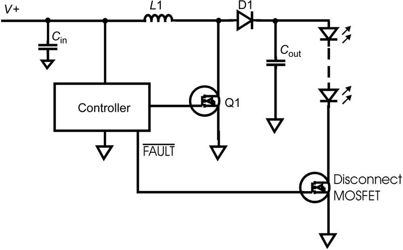
Figure 6.5 Disconnect MOSFET.
The pin is also controlled by the PWM dimming signal, so that the pin is high when the PWM dimming signal is high and vice versa. This disconnects the LEDs and makes sure that the output capacitor does not have to be charged/discharged every PWM dimming cycle. The PWM dimming input to the pin and the output of the protection circuitry are logically AND’ed to make sure that the protection circuit overrides the PWM input to the pin.
Output short circuit protection is provided by a comparator that triggers when the output current sense voltage (at the FDBK pin) is twice that of the reference voltage (at the IREF pin). The output overvoltage protection is activated when the voltage at the OVP pin exceeds 5 V. A fault condition will exist when either of these signals are active and will result in both the GATE pin and the pin being pulled low. Once the IC goes into the fault mode, the capacitor on the COMP pin is used for timing until a reset occurs. At the end of the timing period, the HV9912 will attempt to restart. If the fault condition persists, the HV9912 will continually attempt restarts until power is removed or the fault clears.
Linear dimming is achieved by varying the voltage level at the IREF pin. This can be done either with a potentiometer from the REF pin or from an external voltage source and a resistor divider. This allows the current to be linearly dimmed. However, note that once the voltage at the IREF pin is lowered to a very small value, the offsets of the output short circuit current comparator might cause the HV9912 fault mode to activate improperly. The power to the IC will have to be recycled to start-up the circuit again. To prevent this false triggering, it is advisable to limit the minimum voltage at the IREF pin to about 20–30 mV.
The features included in the HV9912 help achieve a very fast PWM dimming response in spite of the shortcomings of the boost converter. The PWM dimming signal controls three nodes in the IC.
• Gate signal to the switching MOSFET.
• Gate signal to the disconnect MOSFET.
• Output connection of the transconductance op-amp.
When PWMD is high, the gates of both the switching MOSFET and the disconnect MOSFET are enabled. At the same time, the output of the transconductance op-amp is connected to the compensation network. This allows the boost converter to operate normally.
When PWMD goes low, the GATE of the switching MOSFET is disabled to stop energy transfer from the input to the output. However, this does not prevent the output capacitor from discharging into the LEDs, causing a large-decay time for the LED current. This discharge of the capacitor also means that when the circuit restarts, the output capacitor has to charge again, causing an increase in the rise time of the LED current. This problem becomes more prominent with larger-output capacitors. Thus, it is important to prevent the discharge of the output capacitor. This is done by turning off the disconnect MOSFET. This causes the LED current to fall to zero almost instantaneously. As the output capacitor does not discharge, there is no necessity to charge the capacitor when PWMD goes high. This enables a very fast rise time as well.
So what happens if our controller does not have a sample-and-hold switch on the output of the feedback amplifier? When PWMD goes low, the output current goes to zero. This means that the feedback amplifier sees a very large-error signal across its input terminals, which would cause the voltage across the compensation capacitor to increase to the positive rail. Thus, when the PWMD signal goes high again, the large voltage across the compensation network, which dictates the peak inductor current value, will cause a large spike in the LED current. The current will come back into regulation eventually, but how long this takes will depend on the speed of the controller.
The HV9912 disconnects the output of the amplifier from the compensation network when PWMD goes low, which helps to keep the voltage at the compensation unchanged. Thus, when PWMD goes high again, the circuit will already be at the steady state condition, eliminating the large turn-on spike in the LED current.
6.2.3. Multichannel Boost Converters
Some manufacturers have integrated multiple (typically 3) boost converters into a single package. This has been done typically for LCD backlights where one channel is assigned to drive each of red, green, and blue LEDs. Some manufacturers have made four-channel devices; this is because the green color LEDs have a relatively low-light emission, so the channels are assigned red, green, and blue. As green has two channels, the brightness levels are now fairly equal.
To reduce EMI, the channels are usually phased, so that the clock signals are 120-degrees apart in a 3-channel (3-phase) system or 90-degrees apart in a 4-channel (4-phase) system. By phasing there is no large-input current spike as all channels switch at the same time. This would require large-input capacitors for decoupling, to provide this current. In a phased system, the stresses on the input capacitors are reduced and smaller capacitors can be used.
Apart from the phased clocks, each of the boost converters can be considered as a single stage and normal design rules apply.
6.3. Boost Converter Operating Modes
An inductive boost converter can be operated in two modes: either continuous conduction mode (CCM) or discontinuous conduction mode (DCM). The mode of operation of the boost converter is determined by the waveform of the inductor current. Fig. 6.6A is the inductor current waveform for a CCM boost converter, whereas Fig. 6.6B is the inductor current waveform for a DCM boost converter.

Figure 6.6 Inductor current (A) continuous conduction mode (CCM) and (B) discontinuous conduction mode (DCM).
The CCM boost converter is used when the maximum step-up ratio (ratio of output voltage to input voltage) is less than or equal to 6. If larger-boost ratios are required, the DCM boost converter is used. However, in DCM, the inductor current has large-peak values, which increases the core losses in the inductor. Thus DCM boost converters are typically less efficient than CCM boost converters, can create more EMI problems, and are usually limited to lower-power levels.
Inductive boost converters have some disadvantages, especially when used as LED drivers, due to the low-dynamic impedance of the LED string.
• The output current of the boost converter is a pulsed waveform. Thus, a large-output capacitor is required to reduce the ripple in the LED current.
• The large-output capacitor makes PWM dimming more challenging. Turning the boost converter on and off to achieve PWM dimming means the capacitor will have to be charged and discharged every PWM dimming cycle. This increases the rise and fall times of the LED current.
• Open loop control of the boost converter to control the LED current (as in the case of a HV9910-based buck control) is not possible. Closed-loop control is required to stabilize the converter. This also complicates PWM dimming, as the controller will have to have a large bandwidth to achieve the required response times.
• There is no control over the output current during output short circuit conditions. There is a path from the input to the output via a diode and inductor, so turning off the switching MOSFET will have no effect on the short circuit current.
• There will be a surge of current into the LEDs if an input voltage transient raises the input voltage above the LED string voltage. If the surge current is high enough, the LEDs will be damaged.
6.4. Design of a Continuous Conduction Mode Boost Circuit
As a reminder, CCM is valid when the output voltage is between 1.5 and 6 times the input voltage.
6.4.1. Design Specification
Input voltage range = 22–26 V
LED string voltage range = 40–70 V
LED current = 350 mA
LED current ripple = 10% (35 mA)
LED string dynamic impedance = 18 Ω
Desired efficiency > 90%
6.4.2. Typical Circuit
A typical boost converter circuit is shown in Fig. 6.7.

Figure 6.7 Continuous Mode Boost Converter.
6.4.3. Selecting the Switching Frequency (fs)
For low-voltage applications (output voltage < 100 V), and moderate-power levels (<30 W), a switching frequency of fs = 200 kHz is a good compromise between switching power loss and size of the components. At higher voltage or power levels, the switching frequency might have to be reduced to lower the switching losses in the external MOSFET.
6.4.4. Computing the Maximum Duty Cycle (Dmax)
The maximum duty cycle of operation can be computed as

Note: If Dmax > 0.85, the step-up ratio is too large. The converter cannot operate in CCM and has to be operated in DCM to achieve the required step-up ratio.
6.4.5. Computing the Maximum Inductor Current (Iin max)
The maximum input current is

6.4.6. Computing the Input Inductor Value (L1)
The input inductor can be computed by assuming a 25% peak-to-peak ripple in the inductor current at minimum input voltage.

Choose a standard 330-μH inductor. To achieve 90% efficiency at the minimum input voltage, the power loss in the inductor has to be limited to around 2–3% of the total output power. Using a 3% loss in the inductor

Assuming a 80–20% split in the inductor losses between resistive and core losses, the DC resistance (DCR) of the chosen inductor has to be less than

The saturation current of the inductor has to be at least 20% higher than its peak current; otherwise the core losses will be too great.

Thus L1 is a 330-μH inductor with a DCR about 0.38 Ω and a saturation current greater than 1.7 A.
Note: Choosing an inductor with an RMS current rating equal to Iin max would also yield acceptable results, although meeting the minimum efficiency requirement might not be possible.
6.4.7. Choosing the Switching MOSFET (Q1)
The maximum voltage across the MOSFET in a boost converter is equal to the output voltage. Using a 20% overhead to account to switching spikes, the minimum voltage rating of the MOSFET has to be

The RMS current through the MOSFET is

To get the best performance from the converter, the MOSFET chosen has to have a current rating about 3 times the MOSFET RMS current with minimum gate charge Qg. The higher current rating gives low-conduction losses, even at high silicon junction temperatures (resistance increases with temperature). It is recommended that for designs with the HV9912, the gate charge of the chosen MOSFET be less than 25 nC.
The switching device chosen for this application is a 100 V, 4.5 A MOSFET with a Qg of 11 nC.
6.4.8. Choosing the Switching Diode (D1)
The voltage rating of the diode is the same as the voltage rating of the MOSFET (100 V). The average current through the diode is equal to the maximum output current (350 mA). Although the average current through the diode is only 350 mA, the diode carries the full-input current Iin max for short durations of time. Thus, it is a better design approach to choose the current rating of the diode somewhere in between the maximum input current and the average output current (preferably closer to the maximum input current). Thus, for this design, the diode chosen is a 100 V, 1 A Schottky diode.
6.4.9. Choosing the Output Capacitor (Co)
The value of the output capacitor Co (labeled C3 in Fig. 5.8) depends on the dynamic resistance of the LED, the ripple current desired in the LED string and the LED current. In designs using the HV9912, a larger-output capacitor (lower-output current ripple) will yield better PWM dimming results. The capacitor required to filter the current appropriately will be designed by considering the fundamental component of the diode current only.
The output stage of the boost converter is modeled in Fig. 6.8, where the LEDs are modeled as a constant voltage load with series dynamic impedance.

Figure 6.8 Model of Boost Converter Output.
The output impedance (parallel combination of RLED and Co) is driven by the diode current. The waveform of the capacitor current in steady state is shown in Fig. 6.9; the capacitor is charged during the off-time, as the energy stored in the inductor is transferred to the capacitor. Whilst the MOSFET is turned on and energy is being stored in the inductor, the capacitor is discharged by the load.

Figure 6.9 Charge and Discharge Cycle of Output Capacitor.
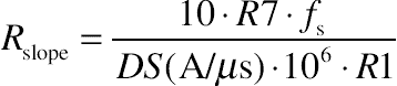
Using the 10% peak-to-peak current ripple given in the design parameters table, the maximum voltage ripple across the LED string has to be
Assuming a constant discharging current of 350 mA when the switch is ON, the equation for the voltage across the capacitor can be written as

Substituting values into this equation, we can calculate the value for Co.

The RMS current through the capacitor can be given by

In this case, a parallel combination of two 1-μF, 100-V metal polypropylene capacitors is chosen.
Note: The proper types of capacitors to use are either metal film capacitors or ceramic capacitors, as they are capable of carrying this high-ripple current. Although ceramic capacitors are smaller in size and capable of carrying the ripple current, they cause a lot of audible noise during PWM dimming as they have a piezoelectric effect. Also, high-value ceramic capacitors are normally only rated up to 50 V. Thus metal polypropylene (or any other metal film) capacitors are the ideal choice for LED drivers if PWM dimming is required.
6.4.10. Choosing the Disconnect MOSFET (Q2)
The disconnect MOSFET should have the same voltage rating as the switching MOSFET Q1. The on-state resistance of the MOSFET at room temperature (Ron,25°C) has to be chosen based on a 1% power loss in Q2 at full-load current. Thus,

The 1.4 multiplication factor is included to account for the increase in the on-resistance due to a rise in junction temperature. In this case, a MOSFET with high-gate charge, Qg, can be chosen if desired (as it is not switching regularly). A high Qg MOSFET will slow down the turn-on and turn-off times. In this case, the MOSFET chosen is a 100 V, 0.7 Ω, SOT-89 MOSFET with a Qg of 5 nC.
6.4.11. Choosing the Input Capacitors (C1 and C2)
The values of input capacitors C1 and C2 have to be calculated to meet closed-loop stability requirements. The connection from the power source to the boost converter circuit will have some resistance, Rsource, and some inductance, Lsource. These feed across the input capacitor (C1 and C2) and so form an LC resonant circuit. To prevent interference with the control loop, the resonant frequency should be arranged to be 40% or less of the switching frequency.
How do we determine the inductance Lsource? A pair of 22AWG connecting wires 1-ft. (30-cm) long will have an inductance of about 1 μH. This is a good starting point. If necessary, the wires can be twisted together to reduce the inductance.
With a 200-kHz switching frequency, the resonant frequency should be less than 80 kHz.

C1 = C2 = 2.2 μF, 50 V ceramic.
The magnitude of the reflected converter impedance at the LC resonant frequency is given by:

6.4.12. Choosing the Timing Resistor (RT)
The HV9912 oscillator has an 18-pF capacitor charged by a current mirror circuit. An external timing resistor RT provides a reference current for the current mirror. When RT is connected to 0 V, current flows and the timing process begins. When charged to a certain voltage, the RS flip-flop is set, the capacitor is discharged, and the timing process starts again. The timing resistor value can be calculated by using the equation:

In this case, for a constant 200-kHz switching frequency, the timing resistor value works out to approximately 270 kΩ. This resistor needs to be connected between the RT pin and GND as shown in the typical circuit.
If using a different controller IC, the equation may have to be modified. For example the HV9911 has a timing capacitor of 11 pF, rather than the 18 pF of the HV9912, so the timing resistor would have to be proportionally larger; that is, 18/11 × 270 kΩ = 442 kΩ.
6.4.13. Choosing the Two Current Sense Resistors (R1 and R2)
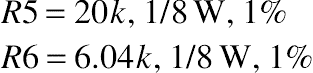
The value of output current sense resistor R2 (Rcs in later calculations) is calculated to limit its power dissipation to about 0.15 W, so that a 1/4 W resistor can be used. Using this criterion,

In this case, the resistor chosen is a 1.24 Ω, 1/4 W, 1% resistor.
The MOSFET current sense resistor R1 (Rs in later calculations) is calculated by limiting the voltage across the resistor to about 250 mV at maximum input current. A 12.5% margin is added to the maximum input current to allow for inductor and other component tolerances.

The power dissipated in this resistor is

Thus, the chosen current sense resistor is a 0.18 Ω, 0.25 W, 1% resistor.
6.4.14. Selecting the Current Reference Resistors (R3 and R4)
The voltage at the current reference pin IREF can be set either by using the reference voltage provided at the REF pin (through a voltage divider) or with an external voltage source. In the present design, it is assumed that the voltage at the IREF pin is set using a voltage divider from the REF pin. The current reference resistors R3 and R4 can be computed using the following two equations:


For this design, the values of the two resistors can be computed to be

6.4.15. Programming the Slope Compensation (Rslope and R7)
As the boost inductor being designed is operating at constant frequency, slope compensation is required to ensure the stability of the converter. The slope added to the current sense signal has to be one-half the maximum down slope of the inductor current to ensure stability of the peak current mode control scheme for all operating conditions. This can easily be achieved by the proper selection of the two slope compensation resistors Rslope and R7.
For the present design, the down slope of the inductor current is

The programming resistors can then be calculated as
Assuming that R7 = 1 kΩ,
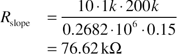
Note: The maximum current that can be sourced out of the SC pin is limited to 100 μA. This limits the minimum value of the Rslope resistor to 25 kΩ. If the equation for slope compensation produces a value Rslope less than this value, then R7 would have to be increased accordingly. It is recommended that Rslope be chosen in the range of 25–50 kΩ.
Based on this recommendation, the calculated values can be scaled by 0.51. The selected resistor values are

6.4.16. Setting the Inductor Current Limit (R5 and R6)
The inductor current limit value depends on two factors, the maximum inductor current and the slope compensation signal added to the sensed current. Another resistor divider, connected to the REF pin, sets this current limit. The voltage at the CLIM pin can be computed as

This equation assumes that the current limit level is set at about 120% of the maximum inductor current Iin max and that the operating duty cycle is at 90% (maximum for the HV9912).
For this design,

We need a potential divider to give 0.36 V from a 1.25 V reference. Using a maximum current sourced out of REF pin of 50 μA the two resistors in series should be >25 kΩ, and can be calculated as:

Note: It is recommended that no capacitor be connected at the CLIM pin because this would affect start-up conditions while it is charging.
6.4.17. Capacitors at VDD and REF pins
It is recommended that bypass capacitors be connected to both VDD and REF pins. For the VDD pin, the capacitor recommended is a 1-μF ceramic chip capacitor. If the design uses switching MOSFETs that have a high-gate charge (Qg > 15 nC), the capacitor value at the VDD pin should be increased to 2.2 μF. Ceramic capacitors have a low impedance, so they are good for supplying a burst of gate drive current.
For the REF pin, the capacitor used is a 0.1-μF ceramic chip capacitor.
6.4.18. Setting the Overvoltage Trip Point (R8 and R9)
The overvoltage trip point can be set at a voltage 15%, or more, above the maximum steady state voltage. Using a 20% margin, the maximum output voltage during open LED condition will be

In the HV9912, the overvoltage comparator input has a 5-V reference. So, the resistors that set the overvoltage set point can be computed as:

This equation will allow us to select a 0.125-W resistor by limiting the power dissipation in the resistor to 0.1 W.

The closest 1% resistor values are

If in a different controller IC, the overvoltage comparator reference voltage is not 5 V, substitute the new value in place of the 5 V used in both previous equations.
Note: The actual overvoltage point will vary from the desired point by ±5% due to the variation in the reference (see datasheet). For this design, it varies from 87.57 to 96.79 V.
6.4.19. Designing the Compensation Network
The compensation needed to stabilize the converter could be either a type-I circuit (a simple integrator) or a type-II circuit (an integrator with an additional pole-zero pair). The type of the compensation circuit required will be dependent on the phase of the power stage at the crossover frequency.
The loop gain of the closed-loop system is given by

Where Gm is the transconductance of the HV9912 internal op-amp (550 μA/V), Zc(s) is the impedance of the compensation network, and Gps(s) is the transfer function of the power stage. Please note that although the resistors give a 1:14 ratio, the overall effect when including the diode drop is effectively 1:15.
For the CCM boost converter in peak current control mode and for frequencies less than 1/10th of the switching frequency, the power stage transfer function is given by

For the present design, choose a crossover frequency 0.01 × fs, fc = 2 kHz. The low crossover frequency will result in large values for Cc and Cz, which will indirectly provide a soft-start for the circuit. As the HV9912 does not depend on the speed of the controller circuit for the PWM dimming response, the low crossover frequency will not have an adverse effect on the PWM dimming rise and fall times.


Substituting s = i·(2π·fc), where fc = 2 kHz, s = i·12,566.

At this frequency, the magnitude and frequency of the power stage transfer function [obtained by substituting s = i·(2π·fc) in the previous equation] are

To get a phase margin of about φm = 45 degrees (the recommended phase margin range is 45–60 degrees), the phase boost required will be

Based on the value of the phase boost required, the type of compensation can be determined.

As we need a 38.57°-phase boost, we need a type-II controller. Note that type-III controllers are usually not required to compensate a HV9912-based boost LED driver and thus will not be discussed further.
The implementations for the type-I and type-II systems for use with the HV9912 are given in Table 6.1.
Table 6.1
Compensation networks
| Type | Circuit Diagram | Transfer Function |
| I |  |
 |
| II |
|

|

The present CCM design needs a type-II controller. The equations needed to design the type-II controller are as follows:


One more equation can be obtained by equating the magnitude of the loop gain to 1 at the crossover frequency.

Transposing this to find Cz + Cc, we get

To summarize the previously obtained results, for substitution:
Rcs (R1) = 0.18
Gm = 550 μA/V
Fc = 2 kHz
K = 2.077
Rs (R2) = 1.22
The result is:
The fault restart (hiccup) time is about 41 ms if Cz + Cc = 41 nF, which is a reasonable value. Earlier we found that ωz = 6,050 and ωp = 26,100, so we can substitute these into the following equation.


Choose

If the MPS boost controller MP4013B were used instead, calculations would have to be repeated with Gm = 370 μA/V. Also because the current sense reference voltages are fixed, new values of Rcs (R1) and Rs (R2) would also need to be substituted into the equations. However, a first approximation for the scaling will be approximately 370/550, giving  .
.
By using previous equations and choosing standard component values, we get:

6.4.20. Output Clamping Circuit
One problem encountered with a continuous mode boost converter, when operating with Vout < 2 × Vin, is L–C resonance between the inductor and Cout. Clamping the output to the input by a diode from Vin to Vout can prevent this resonance. This diode is shown as D2 in Fig. 6.10. Diode D2 can be a standard recovery time diode like 1N4002; this type of diode is better at handling surge currents that may occur at initial switch-on.

Figure 6.10 Boost Converter With Clamping Diode.
This completes the design of the HV9912-based boost converter operating in CCM.
6.5. Design of a Discontinuous Conduction Mode Boost LED Driver
As a reminder, discontinuous mode is used when the output voltage is more than 6 times the input voltage. It is also sometimes used in low power applications when the step-up ratio is less than 6 because compensation is simpler.
6.5.1. Design Specification
Input voltage range = 9–16 V
LED string voltage range = 30–70 V
(Note, with a 9-V input and 70-V output, the Vo/Vin ratio is approximately 7.8.)
LED current = 100 mA
LED current ripple = 10% (10 mA)
LED dynamic impedance = 55 Ω
Efficiency > 85%
6.5.2. Typical Circuit
A typical circuit for a discontinuous mode boost converter, using the HV9912 boost controller IC is shown in Fig. 6.11. This is similar to the continuous mode circuit shown in Fig. 6.7, but uses a simpler compensation circuit.

Figure 6.11 Discontinuous Mode Boost Converter.
6.5.3. Selecting the Switching Frequency (fs)
For low-voltage applications (output voltage < 100 V), and moderate power levels (<30 W), a switching frequency of fs = 200 kHz is a good compromise between switching power loss and size of the components. At higher-voltage or power levels, the switching frequency might have to be reduced to lower the switching losses in the external MOSFET.
6.5.4. Computing the Maximum Inductor Current (Iin max)
The maximum input current is

6.5.5. Computing the Input Inductor Value (L1)
Assuming that the sum of the on-time of the switch and the on-time of the diode is 95% of the total switching time period at Vin min,

Where iLpk is the peak input current (Fig. 6.12).

Figure 6.12 Inductor Current Waveform in DCM.
Vin/L1 controls the rate at which current increases and the rising period is determined by the on-time of the MOSFET, which is the duty cycle multiplied by the switching period. The rate of fall is controlled by (Vo−Vin)/L1 and the falling period is the time that the diode is conducting.
The average input current at the minimum input voltage is equal to the average inductor current and can be computed from

Transposing the equation, the peak input current is

Substituting for iLpk in the equation for L1

Note that the value of L1 computed is the absolute maximum value for the inductor. If the inductor value is larger, the inductor current will flow for longer and the circuit will go into CCM. Assuming a ±20% variation in the inductance, the nominal inductor value has to be

The closest standard value is a 15-μH inductor. This will guarantee DCM operation.
The RMS current through the inductor is

Choose a 15-μH inductor (±20% tolerance). A custom inductor would work best for this application given the large swings in the inductor flux. However, if a standard value inductor is preferred, the saturation current rating of the inductor should be at least 1.5 times the peak current computed, to keep the core losses to an acceptable value. Note that when the circuit is operating at full load, the input current should ramp up linearly. If the rate of current rise increases at the end of the switching cycle, so the ramp is not linear, this indicates that the inductor is beginning to saturate.
The inductor chosen in this case is a 15-μH inductor with an RMS current rating of 1.4 A and a saturation current rating of 3 A.
6.5.6. Computing the On- and Off-Times of the Converter
The on-time of the switch can be computed as

The on-time of diode is

The maximum duty cycle can then be computed as

The diode conduction time ratio can be expressed as

6.5.7. Choosing the Switching MOSFET (Q1)
The maximum voltage across the MOSFET in a boost converter is equal to the output voltage. Using a 20% overhead to account to switching spikes, the minimum voltage rating of the MOSFET has to be
The RMS current through the MOSFET is

To get the best performance from the converter, the MOSFET chosen has to have a current rating about 3 times the MOSFET RMS current with minimum gate charge Qg. It is recommended that for designs with the HV9912 because of limited gate drive capability, the gate charge of the chosen MOSFET be less than 25 nC.
The MOSFET chosen for this application is a 100 V, 4.5 A MOSFET with a Qg of 11 nC.
6.5.8. Choosing the Switching Diode (D1)
The voltage rating of the diode is the same as the voltage rating of the MOSFET (100 V). The average current through the diode is equal to the maximum output current (350 mA). Although the average current through the diode is only 350 mA, the peak current through the diode is equal to iLpk. Thus, it is a better design approach to choose the current rating of the diode somewhere in between the peak input current and the average output current (preferably closer to the peak input current). Thus, for this design, the diode chosen is a 100 V, 2 A Schottky diode.
As the circuit is operating in discontinuous mode, a fast P–N junction diode could be used. An ultrafast Schottky diode is not required to keep the switching losses low. However, a Schottky diode does have a low-forward voltage drop, so conduction losses are lower that for a P–N junction diode. If cost is more important that efficiency, use a fast P–N junction diode.
6.5.9. Choosing the Output Capacitor (Co)
The value of the output capacitor depends on the dynamic resistance of the LED string, as well as the ripple current desired in the LED string. In designs using the HV9912, a larger-output capacitor (lower-output current ripple) will yield better PWM dimming results. The capacitor value needed to filter the output ripple current will be calculated by considering the RMS current through the LED load.
The output stage of the boost converter is modeled in Fig. 6.13, where the LEDs are modeled as a constant voltage load with series dynamic impedance.

Figure 6.13 Model of Boost Converter Output.
The waveform of the capacitor current in steady state is shown in Fig. 6.14.

Figure 6.14 Output Capacitor Current.
Using the 10% peak-to-peak current ripple given in the design parameters table, the maximum voltage ripple across the LED string has to be

Assuming a constant discharging current of 350 mA when the diode current is zero, the equation for the voltage across the capacitor can be written as
Substituting values into this equation,

The RMS current through the capacitor can be given by

In this case, a parallel combination of two 1 μF, 100 V metal polypropylene capacitors is chosen.
Note: The proper type of capacitors to use is either metal film capacitors or ceramic capacitors, as they are capable of carrying this high-ripple current. Although ceramic capacitors are smaller in size and capable of carrying the ripple current, they cause a lot of audible noise during PWM dimming. High-value ceramic capacitors are usually limited to 50-V rating. Thus metal polypropylene (or any other metal film) capacitors are the ideal choice for LED drivers if PWM dimming is required.
6.5.10. Choose the Disconnect MOSFET (Q2)
The disconnect MOSFET should have the same voltage rating as the switching MOSFET Q1. The on-state resistance of the MOSFET at room temperature (Ron,25°C) has to be calculated based on a 1% power loss in Q2 at full-load current. Thus,

The 1.4 multiplication factor is included to account for the increase in the on-resistance due to rise in junction temperature. In this case, a high Qg MOSFET can be chosen if desired (as it is not switching regularly), but a high Qg MOSFET will slow down the turn-on and turn-off times (which might be allowable based on PWM dimming frequency). In this case, the MOSFET chosen is a 100 V, 0.7 Ω, SOT-23 MOSFET with a Qg of 2.9 nC.
6.5.11. Choosing the Input Capacitors (C1 and C2)
The values of input capacitors C1 and C2 have to be calculated to meet closed-loop stability requirements. The connection from the power source to the boost converter circuit will have some resistance, Rsource, and some inductance, Lsource. These feed across the input capacitor (C1 and C2) and so form an LC resonant circuit. To prevent interference with the control loop, the resonant frequency should be arranged to be less than 40% of the switching frequency.
A pair of 22AWG connecting wires 1-ft. (30-cm) long will have an inductance of about 1 μH. This is a good starting point. If necessary, the wires can be twisted together to reduce the inductance.
With a 200-kHz switching frequency, the resonant frequency should be less than 80 kHz.
C1 = C2 = 2.2 μF, 50 V ceramic.
The maximum source impedance is found using:


6.5.12. Calculating the Timing Resistor (RT)
The HV9912 oscillator has an 18-pF capacitor charged by a current mirror circuit. An external timing resistor RT provides a reference current for the current mirror. When RT is connected to 0 V, current flows and the timing process begins. When charged to a certain voltage, the RS flip-flop is set, the capacitor is discharged, and the timing process starts again. The timing resistor can be calculated by using the following equation:
In this case, for a constant 200-kHz switching frequency, the timing resistor value is approximately 270 kΩ. This resistor needs to be connected between the RT pin and GND as shown in the typical circuit.
6.5.13. Calculating the Two Current Sense Resistors (R1 and R2)
The value of the output current sense resistor R2 can be calculated by limiting its voltage drop to below 0.4 V. Using this criterion,

The power dissipation will be 0.4 V × Io max = 0.04 W. In this case, the resistor chosen is a 3.9 Ω, 1/8 W, 1% resistor.
The MOSFET current sense resistor R1 is calculated by limiting the voltage across the resistor to about 250 mV at maximum input current.

The power dissipated in this resistor is

Thus, the chosen current sense resistor is a 0.12 Ω, 1/4 W, 1% resistor.
6.5.14. Selecting the Current Reference Resistors (R3 and R4)
The voltage at the current reference pin IREF can be set either by using the reference voltage provided at the REF pin (through a voltage divider) or with an external voltage source. In the present design, it is assumed that the voltage at the IREF pin is set using a voltage divider from the REF pin. The current reference resistors R3 and R4 can be computed using the following two equations:


For this design, the values of the two resistors can be computed to be

6.5.15. Setting the Inductor Current Limit (R5 and R6)
The inductor current limit value depends on two factors: the maximum inductor current and the slope compensation signal added to the sensed current. Another resistor divider from the REF pin (R5 and R6) is connected to the CLIM pin and sets the maximum inductor current. The voltage at the CLIM pin can be computed as
This equation assumes that the current limit level is set at about 120% of the maximum inductor current Iin max.
For this design,

Using a maximum current sourced out of REF pin of 50 μA, the two resistors can be calculated as
No capacitor should be connected at the CLIM pin because this will affect the circuit at start-up.
6.5.16. Capacitors at VDD and REF Pins
It is recommended that bypass capacitors be connected to both VDD and REF pins. For the VDD pin, the capacitor used should be a 10-V ceramic chip capacitor. For low-power designs, a 1-μF capacitor is adequate. If the design uses high-gate charge switching MOSFETs (Qg > 15 nC), the capacitor at the VDD pin should be increased to 2.2 μF.
For the REF pin, the capacitor used is a 0.1-μF ceramic chip capacitor.
6.5.17. Setting the Overvoltage Trip Point (R8 and R9)
The overvoltage trip point can be set at a voltage 15% higher than the maximum steady state voltage. Using a 15% margin, the maximum output voltage during open LED condition will be:

Then, the resistors that set the overvoltage set point can be computed as

This equation will allow us to select a 1/8-W resistor by limiting the power dissipation in the resistor.

The closest 1% resistor values are

Note: The actual overvoltage point will vary from the desired point by ±5% due to the variation in the reference (see datasheet). For this design, it varies from about 76.5 to 84.5 V. As the maximum output voltage is designed to be 70 V, we have at least 6.5-V margin.
The HV9912 uses a 5-V reference voltage for the OVP comparators, which is why 5 V appears in the equations for R8 and R9. In boost controllers where this reference voltage is different, such as the LTC3783 that uses 1.23 V, this value should be substituted for 5 V.
6.5.18. Designing the Compensation Network
The compensation needed to stabilize the converter could be either a type-I circuit (a simple integrator) or a type-II circuit (an integrator with an additional pole-zero pair). The type of the compensation circuit required will be dependent on the phase of the power stage at the crossover frequency.
The loop gain of the closed-loop system is given by

Where Gm is the transconductance of the op-amp (550 μA/V), Zc(s) is the impedance of the compensation network, and Gps(s) is the transfer function of the power stage. Please note that although the resistors give a 1:14 ratio, the overall effect when including the diode drop is effectively 1:15.
To compute the transfer function for the DCM boost converter in peak current control mode, we need to define a couple of factors.


For frequencies less than 1/10th of the switching frequency, the power stage transfer function is given by


For the present design, choose a crossover frequency ∼0.01 fs, or fc = 2 kHz. The low-crossover frequency will result in large values for Cc and Cz, which will indirectly provide a soft-start for the circuit. As the HV9912 does not depend on the speed of the controller circuit for the PWM dimming response, the low-crossover frequency will not have an adverse effect on the PWM dimming rise and fall times. By substituting s = i·(2π·fc) = i·12,566 into the transfer function, we get:

The magnitude and frequency of the power stage transfer function are:

To get a phase margin of about φm = 45 degrees (the recommended phase margin range is 45–60 degrees), the phase boost required will be

Based on the value of the phase boost required, the type of compensation can be determined.

A type-I controller is required to compensate a HV9912 in discontinuous mode. This is much easier to design compared to the type-II compensation described earlier for CCM operation (Table 6.1).
So, for the present design, a simple type-I controller will suffice. The following equation is for the loop gain:

All that is needed is to adjust the gain of the loop to be 1 at the crossover frequency. Transposing this equation, we obtain the value of Cc that will be needed to achieve this.

Reminder of previous results:
R2 (Rs) = 3.9
R1 (Rcs) = 0.12
Gm = 550 μA/V
ωc = 12,566
Aps = 0.039
So, but substitution:

Choose Cc = 3.9 nF, 50 V, C0G capacitor
This completes our DCM boost converter design using the HV9912. If you are using the LTC3783 boost controller from Linear Technology, Gm = 588 μA/V, so upscaling gives a Cc value of 3.95 nF; hence 3.9 nF could be used, as the HV9912 design. If instead you are using the MP4013B boost controller IC from MPS, Gm = 370 μA/V so the value of Cc should be scaled down accordingly (2.49 nF; use the nearest standard value of 2.2 nF or 2.7 nF).
6.6. Common Mistakes
1. The most common mistake is not having adequate OVP at the output. If the LEDs are disconnected while the circuit is operating, the output voltage will rise until components start to break down. The overvoltage limit set at the output of the boost converter should be lower than the breakdown voltage of any component connected across it. However, in some low-cost, sealed backlight modules, OVP is not provided because the circuit is deemed unrepairable.
2. Testing the circuit with a short string of LEDs. In this case, the forward voltage drop of the LEDs may be lower than the supply voltage, so there will be a high-current flow and the LEDs are likely to be destroyed.
3. Using multilayer ceramic capacitors across the output when PWM dimming will be used. Multilayer ceramic capacitors are piezoelectric, so PWM dimming will cause an audible whistle to be produced.
6.7. Conclusions
Boost converters are used when the minimum output voltage is at least 1.5 times the input voltage. Below this step-up ratio, buck–boost converters should be used instead. These will be described in the next chapter.
CCM is recommended for applications with low input to output step-up ratios, when the output voltage is a maximum of 6 times the input voltage. This keeps the EMI levels relatively low, although care should still be taken in PCB layout and filtering.
DCM is necessary if the output voltage is more than 6 times the input voltage. In some applications, discontinuous mode is used at low step-up ratios because compensation calculations are easier. However, but the EMI produced by a discontinuous mode boost converter is much higher than for a CCM boost converter of similar power output.
..................Content has been hidden....................
You can't read the all page of ebook, please click here login for view all page.