Improving embedded Flash memory technology: silicon and metal nanocrystals, engineered charge-trapping layers and split-gate memory architectures
G. Molas and L. Masoero, CEA-LETI, France,
V. Della Marca, STMicroelectronics, France
G. Gay and B. De Salvo, CEA-LETI, France
Abstract:
This chapter presents an overview of the charge trap, silicon nanocrystals and split-gate memory technologies, which are currently envisaged as promising solutions to solve the scaling issues of standard embedded Flash memory technologies. In particular, we will focus on the main features allowing improved performance and scaling perspectives. We will also discuss in detail the main key challenges of these promising emerging technologies with particular focus on reliability issues.
Key words
charge trap memories; embedded memories; nanocrystals; silicon nitride; high-k control dielectrics; split-gate memory architecture
4.1 Introduction
Embedded non-volatile memories are finding increasing use in a wide array of ICs, with applications ranging from a few bits (analog trimming) to a few Megabits for data/code storage (Bergemont 2007). Embedded memories have played a crucial role in developing reliable, high performance microcontrollers. The embedded memories are integrated with bulk logic CMOS technology. Two key application areas that are driving advances in embedded Flash technologies are automotive microcontrollers and smart cards (Strenz 2011) Automotive market specifications are very stringent. The temperature range application is broad (− 40 to 175 °C). The fail rate should be also extremely well controlled (< 1 ppm over 15–20 years). The required memory size and performance are expected to grow exponentially in the future, with densities of up to several Mbytes and access times of 10 to 20 ns (Strenz 2011). For smart cards, 1 to 5 ms fast erase speed and low power consumption (especially for contactless applications) are required. In this context, the diverse requirements make it difficult for one cell type to cover all the needs of the various applications (Baker 2012). Indeed, today three main concepts dominate the market, depending on the application key challenges:
• 2T EEPROM Floating Gate memory (Lee et al. 2008): offers low power due to the Fowler-Nordheim/Fowler-Nordheim program erase, but have a large cell size and high voltages;
• 1T NOR stacked gate concept (Piazza et al. 2010): the 90 nm technology was introduced in the market by STMicroelectronics in 2007. This solution is highly reliable and enables small cell size but suffers from high programming currents and elevated voltages;
• Different Split-gate concepts: can be integrated with Poly-Si floating gate: as in the SST/TSMC SuperFlash (Liu et al. 2006) and Infineon/TSMC HS3P (Shum et al. 2012) or with a discrete charge trapping layer: as in the Renesas 1.5T Flash MONOS with SiN trapping layer (Ito et al. 2004) and in the Freescale Thin Film Storage technology with a Silicon Nanocrystals trapping layer (Kang et al. 2012). These structures offer low consumption due to the use of the Source Side Injection programming mode.
The embedded market is pushing for highly reliable memories for the next generations. However, several key challenges are making scaling difficult (Strenz 2011):
• stringent requirements in terms of high temperature retention, reduced fail bits and improved endurance. On the other hand, low power consumption is also a key point for some applications;
• compatibility with advanced logic CMOS nodes, mostly based on high-k/metal gate technology beyond 28 nm;
• clear slowdown of the memory area shrink potential (due to the high programming voltages) in parallel to an increase in the wafer cost (beyond the 45 nm) gives rise to a critical saturation of the chip cost for classical bit cell concepts.
For these reasons, innovative and alternative technologies (in particular emerging Back-End Resistive RAMs) are currently under investigation for advanced memory nodes. Nevertheless, the stringent reliability requirements and manufacturing challenges make these solutions unviable for the embedded memory market. Strong efforts (both in research labs and in semiconductor companies) are still devoted to push further the scaling limits of standard eNVM technologies. In this context, the objective of this chapter is to present a review of the potential, challenges and opportunities of some evolutionary approaches. These approaches will allow us to scale further the standard embedded memories and improve device performances. In particular we will focus on charge trap memories, silicon nanocrystal memories and split-gate architectures.
4.2 Silicon nanocrystals
4.2.1 Technological optimization of Si-nc memories
The silicon nanocrystal (Si-nc) Flash memory cell appears as a promising candidate for embedded applications, due to its good reliability (resistance to SILC, no tail-bits) and ease of integration (Compagnoni et al. 2003; De Salvo et al. 2003). The idea is to replace the continuous Poly-Si floating gate with a discrete charge trapping layer composed of nanometer-size silicon nanocrystals (Fig. 4.1). This will avoid the fully discharging of the storage medium in case of defect-related leakage paths in the tunnel oxide.

Technological optimization of Si-nc memories has been the subject of many studies in the literature. In particular, the optimization of the nanocrystal features (size and density) introduced improvements to the memory performances at the array level (Jacob et al. 2008). It was shown that using a hybrid Si-NC/SiN charge trapping layer leads to a higher memory window (Molas et al. 2007), but with a degradation of the retention time at elevated temperatures. The integration of high-k in the control dielectric stack reduces the programming voltages and facilitates the Fowler-Nordheim operation (Molas et al. 2007). Most recent results have shown that other architectures, such as split-gate memories (Masoero et al. 2011a; Yater et al. 2011) (Section 4.5.2), are suitable for energy consumption reduction of the memory, but require the addition of a select transistor, controlling the programming current.
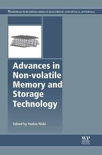
In Si-nc memories, a tunnel oxide thickness of more than 4.2 nm is required to achieve 10 years of data retention at 150 °C (Fig. 4.2). Increasing the nano-crystal size allows an increase in the coupling ratio of the memory cell, and thus the memory window (Della Marca et al. 2012). Figure 4.3 presents the programming and cycling characteristics of Si-nc memories for two nano-crystal sizes, maintaining the discrete character of the charge trapping layer. Large 12 nm nanocrystals can reach a 4 V memory window after 106 cycles (Fig. 4.4)).


4.2.2 Programming scheme optimization of Si-nc memories
Further improvements in Si-nc memory performances can be obtained by optimizing the programming conditions in Hot Carrier mode, namely the drain and gate biases and the pulse shape (box vs ramp) and duration (Della Marca et al. 2013). Figure 4.5 shows the programming energy plotted as a function of the programming window for various programming conditions. The box pulse can increase the programming window while the energy consumption and the biasing conditions are kept constant. At the beginning of the programming time, the abrupt variation of Vg can start the hot carrier generation. Using a ramp, the hot electron injection starts when Vg ≈ Vd, thus allowing for the programming efficiency to be lower. The programming window tends to saturate, leading to higher required programming time. This is due to the quantity of injected charges that modify the vertical electric field during the programming operation. The programming efficiency was defined with these results as the ratio between the programming window and energy consumption. Figure 4.6 shows the programming efficiency in the case of box pulse for different biasing conditions; it also shows the linear dependence with the gate voltage (or vertical electric field).


On the other hand, an optimized efficiency is measured for Vd = 4.2 V. When the drain voltage is higher than 4.2 V, the programming injection tends to saturate while the drain current increases. This increases the consumption and reduces the programming efficiency. Finally, Fig. 4.7 shows the consumed energy as a function of the programming window. Depending on the final purpose, it is possible to decrease the programming time in order to reduce the energy consumption for very fast and ultra low energy applications.

4.2.3 Si-nc engineering
One of the issues of Si-nc memories is the limited memory window. Two solutions can be proposed to improve the ΔVT of the memory: metal nanocrystals to increase the number of charges stored (larger density of states and larger work function), and the use of two stacked Si-nc layers to increase the number of trapping sites.
Si-nc double layer
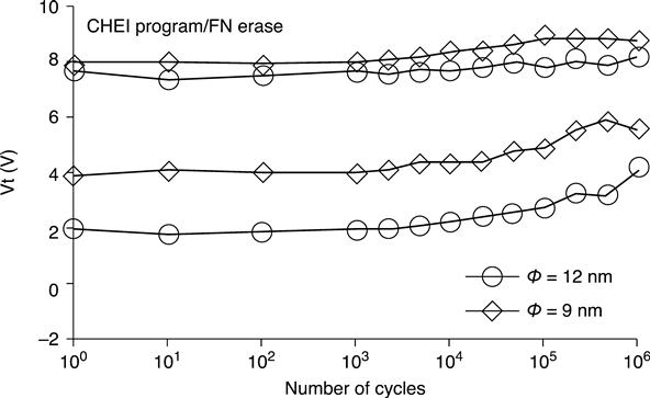
Using two stacked-Si-nc layers is a conservative solution (i.e. based on S-nc), which increases the number of trapping sites of Si-nc memories, and thus the memory window. This is done by integrating a double layer of silicon nanocrystals as a trapping medium and combining it with a high-k-based control dielectric (Gay et al. 2009, 2010a,b,c). The two Si-ncs stacked layers were deposited by CVD (medium diameter ϕ ~ 6 nm, dot density d = 9 × 1011 cm− 2) and separated by less than 2 nm-thick HTO. The second Si-nc layer was passivated by a 750 °C NH3 nitridation. A HTO/HfAlO/HTO tri-layer control dielectric plus poly-Si control gate was used.
Write/Erase (W/E) characteristics of Si-nc single and double layer memories are presented in Fig. 4.8. The memory window is improved (ΔVT is increased by 50% at Vg = ± 17 V 2 ms), while the charge trapping layer remains discrete. It was found that erasing is faster in the case of the Si-nc double layer.
The charging phenomenon was modelled with a simple floating gate-like approach (De Salvo 2001), in which the electrostatic influence of the charged Si-nc on the channel is proportional to a factor called Rdot. This represents the covering ratio of Si-nc on the device active area. By fitting the experimental W/E characteristics of the Si-nc memories with our model (with the same parameters for both devices), a Rdot of 60% is extracted for single layer Si-nc memories, while an effective Rdot of 90% is reached for double layer Si-nc devices (Fig. 4.9). A Rdot close to 100% means that the double layer Si-nc is electrically equivalent to a continuous Poly-Si floating gate layer. As a consequence, double layer Si-nc combines the discreetness of nanocrystals floating gate and the full channel coverage of continuous Poly-Si floating gate devices. Concerning the memory programming, adding a second nanocrystals layer is equivalent to increasing the nanocrystals density.

It appears that over-erasing on the Si-nc double layer device occurs with these W/E characteristics, which cannot be explained by the floating gate-like model. Indeed, single layer Si-nc Vt is saturated at the threshold voltage of the virgin cell during erasing, while double layer Si-nc Vt is shifting under virgin Vt. This means that positive charges are stored in the gate stack after erasing, thus leading to over-erasing. This phenomenon can be explained by the extraction of electrons from the top Si-nc layer valence band. The silicon oxide separating the two silicon-ncs layers is 2 nm thick. Despite the large Si valence band/silicon oxide barrier height (4.2 eV), the thinness (2 nm) of the inter-layer oxide makes the valence band electrons tunnel from the top Si-nc to the bottom Si-nc layer conduction band. These electrons leave behind a hole in the top Si-nc layer valence band. The two models: (i) floating gate-like model; and (ii) valence band electron tunneling, are compared to the experimental W/E characteristics (Fig. 4.10). In the model without valence band electron tunneling, the erased Vt is saturating to the virgin Vt. However, when valence electron tunneling is taken into account, erased Vt is below virgin Vt (dashed curve). The 1.1 V over-erasing explained by the valence band tunneling model fits well with the over-erasing measured on the devices.

The memory window increase due to the Si-nc double layer can be explained by two phenomena. The larger channel area surface coverage (Rdot) explains around 50% of the memory window boost. The other approximately 50% are attributed to valence-band electron tunnelling from the top Si-nc layer leaving holes in the top Si-nc layer during erasing, leading to an increase of the erasing speed and to over-erasing.
4.3 Metal nanocrystals
Metal nanocrystals (ncs) advantages are:
• a large density of states around Fermi level;
• the absence of band splitting; and
• the work function engineering, due to the large choice of available metals.
One way to obtain a dense metal ncs array is to deposit a thin metal layer by physical vapor deposition (Choi 2005; Dufourcq et al. 2008; Lee et al. 2005), which is then annealed to form the nc array. Major concerns about metal ncs are their poor thermal stability (Singh et al. 2009) and their incompatibility with MOSFET processes, since they can induce metal contamination in front end tools and in the memory gate stack. To solve this problem, one solution is to use MOSFET compatible metals such as W (Lim et al. 2005) and TiN (Lu et al. 2009; Maikap et al. 2008), both deposited by atomic layer deposition. Since these metals are very sensitive toward oxidation, blocking dielectrics are deposited in situ on top of the ncs, without exposition to the ambient atmosphere.
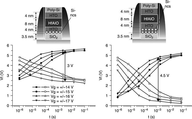
A silicon passivation process makes TiN ncs robust toward ambient air oxidation and allows for depositing ncs and blocking dielectrics in different tools (Gay et al. 2010b]. It is best to couple the SiN trapping layer concept with that of metal ncs. The SiN acts as a diffusion barrier for TiN and as an additional trapping layer. The integration can be demonstrated in a full MOSFET process of Si-passivated CVD TiN ncs encapsulated in a SiN matrix. TiN ncs deposition and passivation are performed in an 8 inch industrial CVD Centura tool. TiN ncs are deposited on a 4 nm thermal silicon oxide at 680 °C with precursors TiCl4 and NH3, as follows:
[4.1]
Ncs are then exposed to dichlorosilane at 550 °C, in order to selectively deposit a silicon shell around the ncs. Finally, they are exposed to NH3 at 680 °C, which creates a thin nitride layer at the surface of the silicon shell. At this step, TiN ncs are passivated against oxidation and can now be exposed to the ambient atmosphere. Nc density is estimated by TEM to be of 3 × 1012 cm− 2 and has a mean diameter of 3.5 nm, corresponding to a surface coverage of around 30%. Once TiN and TiO2 based nc-memories were processed, a 16 nm Al2O3 control dielectrics is deposited by ALD, followed by a 1 minute annealing at 1050 °C in N2. Afterwards, a PVD TiN/poly-Si control gate was deposited. In energy filtered mode centred on titanium, TiN ncs are clearly identified by a bright line, with no titanium diffusion detected in the gate stack (Fig. 4.11).
At 1 ms programming and erasing time (Vg = ± 18 V), an 8 V memory window is obtained. Erasing dynamics of the memory device is compared to the two reference devices with non-passivated ncs (TiO2) and SiN layer without ncs (Fig. 4.12). Devices with TiN ncs are erased 102 faster than devices with a pure SiN layer. This is an important result, since one weakness of nitride trap memory devices is their bad erasing speed. The enhanced erasing between devices without ncs and devices with ncs is explained by enhanced electrostatics in the SiN under the ncs due to the spherical shape of the ncs. Because of the high dielectric permittivity of both TiN and TiO2, the electric field is equal to zero inside the ncs. Consequently, isopotential lines are squeezed around the ncs, inducing a local increase of the electric field under the ncs (Fig. 4.12(d)). The presence of the nc induces a boost of the electric field in the SiN bottom layer. At the inter-face between SiN and the nc, the electric field reaches the maximal value of 17 MV cm− 1. This is three times higher than the electric field in the absence of nc. This enhanced electric field is producing a band bending in the SiN layer, which is boosting the erasing by promoting electrons migration to the SiN/SiO2 interface (Fig. 4.12(c)).

In parallel, the additional erasing enhancement between the TiO2 ncs device and the TiN ncs device is due to additional electrons tunnelling from the TiN ncs to the substrate. This explains the 1.2 V over-erasing observed on the devices with TiN ncs.
4.4 Charge trap memories
Charge trap memories, essentially based on silicon nitride (SiN) charge trapping layers, are also promising alternative candidates for embedded memories. This is due to their ease of integration and low program erase voltages. However, they generally suffer from insufficient retention at high temperatures. In order to improve their performances, engineering of the gate stack is proposed in the literature.
4.4.1 New materials for charge trap memories
Tunnel oxide engineering
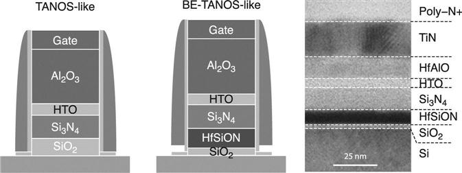
In order to reduce the program erase voltages of charge trap memories, the integration of a Band-Engineered (BE) tunnel barrier can be proposed. Various solutions, based on different materials, were investigated in the literature (Lai et al. 2007; Lue 2008; Van Schaijk et al. 2006; Verma et al. 2009). In particular HfSiON is a good candidate to be integrated in the tunnel stack of TANOS memories due to its low trap concentration. Indeed, the presence of defects in the tunnel layer is a critical point and can degrade the retention of the memory. This is more so at high temperatures.
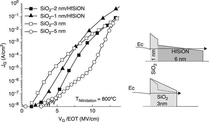
The tunnel stack proposed here is composed of a 6 nm HfSiO (Hf/Si ~ 60/40) deposited by MOCVD on an approximate 1 nm thermal SiO2 as a tunnel stack (Molas et al. 2010). HfSiO was nitridated with NH3 at 800 °C (yielding HfSiON), in order to increase the crystallization temperature and reduce the parasitic trapping in the tunnel stack. Si3N4 is used as a trapping layer and HTO/Al2O3 as control dielectrics (Fig. 4.13). Figure 4.14 shows the IV characteristics of a SiO2/HfSiON bi-layer. Compared with the SiO2 reference, a higher electron injection is measured at high voltages (increasing the programming speed), while a lower leakage current is measured at low voltages (reducing the charge loss during the retention mode). This demonstrates the engineered tunnel barrier effect of the SiO2/HfSiON bi-layer, suitable for tunnel oxide applications. Figure 4.15 shows the Program Erase characteristics of a BE-TANOS memory integrating HfSiON in the tunnel stack. A much higher memory window (ΔVT of 4 V with 16 V 100 μs/-16 V 1 ms PE conditions) is measured compared to the reference with SiO2 tunox. In fact, the high electron injection given by the SiO2/HfSiON bi-layer tunnel oxide boosts the program/erase speeds.

Engineered nitride charge trapping layers
Engineered nitride charge trapping layers, with different material stoichiometry, are being researched to replace the standard Si3N4 material (Van den Bosch et al. 2008; Vianello et al. 2009). Alternative materials are proposed in order to improve the material trap depth and density (Chin et al. 2005; Lin et al. 2006; Huo et al. 2007). In particular, AlN was proposed due to its high trapping capabilities, high band gap and elevated electron affinity (Chakraborty et al. 2009; Chin et al. 2006).
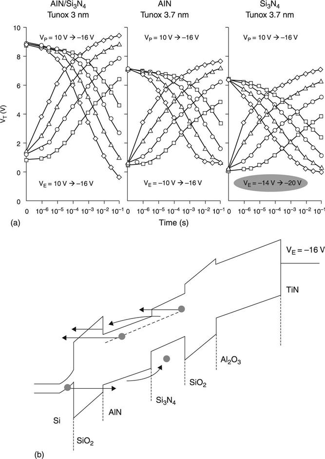
The comparison between Si3N4, AlN and AlN/Si3N4 charge trapping layers (Molas et al. 2010b, 2011) in memory structures, employing SiO2/Al2O3 control dielectrics and TiN control gate, is shown in Fig. 4.16. The lateral grain size was estimated to be approximately 2 nm. CV measurements were performed on devices with various AlN thicknesses from 6 nm to 14 nm, and allowed to extract a dielectric constant of approximately 9 to 10 at the end of the integration process. Ellipsometry and Ultra-violet photoelectron spectroscopy (UPS) measurements performed on AlN layers allowed to extract respectively a band gap of 6.2 eV and an electron affinity of 3.1 eV (Fig. 4.16). In comparison with Si3N4, AlN exhibits a slightly higher dielectric constant, a higher band gap and a more elevated electron affinity. AlN/Si3N4 charge trapping double layers were investigated, the objective being to combine fast erase and good retention.

Figure 4.17 presents the program erase characteristics of the AlN, Si3N4 and AlN/Si3N4 storage layers. AlN/Si3N4 memories exhibit a larger memory window with respect to charge trapping single layers. For respective PE conditions of 16 V/100 ls and − 16 V/10 ms, the memory window is increased from 3 V with Si3N4 to 6.5 V for AlN/Si3N4. In particular, little difference is measured between the different stacks. At short programming times, AlN/Si3N4 shows a slightly slower programming speed resulting from a thicker EOT of 2 to 3 nm. However, the maximum programmed VT is higher due to a higher number of trapping sites. AlN/Si3N4 erasing offers reduced erase saturation in comparison with AlN erasing, due to the thicker equivalent charge trapping layer. It was also noticed that the erasing speed of AlN/Si3N4 is much faster than that of Si3N4 devices. This can be explained by the band diagram of the structure. The AlN layer offers intermediate energy states for the electrons trapped in the Si3N4 layer, and thus accelerates the erasing mechanism. Moreover, the band diagram of AlN/Si3N4 double layers is favourable for hole injection to compensate for the charges trapped in Si3N4 (Fig. 4.17). Finally, reference memory devices with Si3N4 AlN charge trapping double layers (instead of AlN/Si3N4) showed much slower program erase dynamics for similar EOT. This important result underlines the band engineered effect in AlN/Si3N4 charge trapping layers, and confirms that the AlN bottom layer improves the PE speed of the memory.
The charge loss rate of the programmed state is of approximately 70 mV/decade at 125 °C was measured. More than 90% of the charge remains trapped after 10 years, leading to a memory window of more than 5 V. The small charge loss rate can be explained by the additional energy barrier seen by the electrons trapped in the nitride layer. This is due to the additional AlN bottom layer (Fig. 4.18). Using a thick charge trapping layer allows improving retention up to moderate temperatures (Bocquet et al. 2009). In conclusion, the improved retention behaviour combined with the faster erase with respect to AlN and Si3N4 single layers demonstrates the band engineered effect of the AlN/Si3N4 charge trapping layer. Figure 4.18 presents the cycling characteristics of an AlN/Si3N4 charge-trap memory. A constant memory window of approximately 5 V is kept after 106 cycles. Once again, this proves the advantage of an additional AlN layer to ease the electron removal from the Si3N4 during the erasing procedure. Finally, we can notice that a very small VT drift (~ 500 mV for the erased state after 106 cycles) is measured in these devices.

4.4.2 Optimization of Al2O3 interpoly-dielectric in charge trap memories
In embedded memories, the ease of co-integration of the memory technologies with the micro-controllers logic CMOS is the most important requirement. The cell size shrink is not primordial, as it is the stand-alone memories and relaxed memory structures can be adopted for embedded applications. However, if the high write/erase voltages could be reduced, the area consuming high voltage peripheral Flash circuitry may also be shrunk along with the cell array. For this purpose, replacement of the traditional ONO interpoly with a high-k dielectric material represents a promising approach for achieving a considerable shrink of the full memory array without impacting process complexity. Here we focus on Al2O3 for the control dielectric or interpoly applications (Masoero 2011b; Molas et al. 2010c). Process innovations of Al2O3 are required to reduce the leakage current through the layer and improve the retention performances. For this to work, the microscopic nature of traps in Al2O3 and correlating the Al2O3 defects and the retention behaviour of charge-trap memories needs to be addressed.
In order to model the defects in Al2O3, first principle calculations using the SIESTA code were used (Sanchez-Portal et al. 1997). This was mainly based on the density functional theory (DFT) using Local Spin Density Approximation (LSDA) and a linear combination of atomic orbitals. A supercell of 160 atoms was used to model the γ-alumina (Menéndez-Proupin and Gutiérrez, 2005) (Fig. 4.19). It is the crystalline phase that is identified after an annealing step during the device fabrication process of the ALD Al2O3 layers (Molas et al. 2010c).
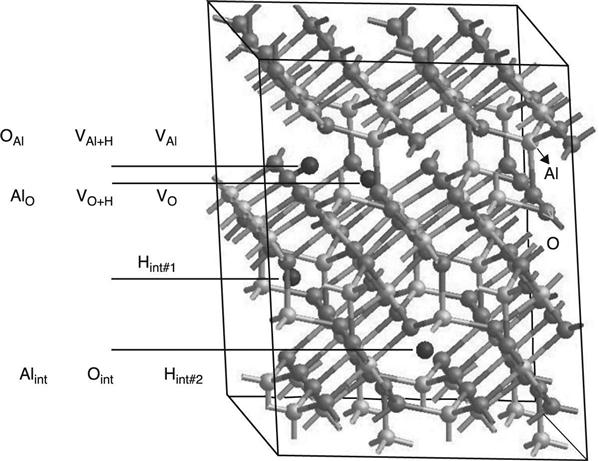
In order to determine the most relevant defects that can play a role in the memory device, attention was focused on the position of the electronic levels with respect to the band gap of bulk γ-Al2O3. Also the Gibbs formation energy that primarily governs the concentration of defects inside the deposited film was another area of focus. Two kinds of defects were considered: intrinsic oxide point defects and hydrogenated defects. The latter are motivated by the fact that hydrogen is an ubiquitous impurity in all fabrication processes.
The results of many calculations are presented in this work: the aluminium, oxygen and hydrogen interstitials (Alint Oint Hint) in different sites of the defective spinel structure; the oxygen and the aluminium vacancies (VO and VAl) possibly passivated with H (VO + H and VAl + H); the substitutional defects Al replaced with O and vice versa OAl and AlO. The formation energies were calculated from the total energy of a defective supercell as a function of the oxygen chemical potential. For a quasi-stoichiometric c-alumina, the VO is the most stable among the different considered point defects (Fig. 4.20). For an oxygen-rich alumina, but less favourable in the samples conditions (Colonna et al. 2011), OAl and Oint could also be considered as they provide energy levels close to the conduction band. Moreover Oint for a stoichiometric alumina is less stable than VO, but remains one of the most stable γ-Al2O3 active defects with a Gibbs free energy. This is comparable to that of Hint at high pressure and temperature conditions.

The oxygen vacancy can usually exist in all five charged states from − 2 to + 2. The computed DOS of VO in these charged states is reported in Fig. 4.21. In the D0 state, VO introduces a vacant level slightly above the conduction band. This is unlikely to participate to electrical conduction. However, even by opening the band gap correctly, GW calculations confirmed the behaviour reported in Liu and Robertson (2009): the energy level decreases below the CB only when the trap is progressively charged by electrons. It can thus be imagined that if VO plays a role in trap assisted conduction, it would be with D- and D2- states.

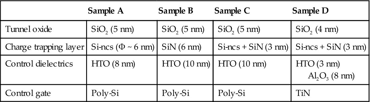
The study of H-related defects in c-Al2O3 was motivated by the presence of H-atoms in the layer, as evidenced by SIMS measurements (Fig. 4.22). Among all the possible H-related defects, the interstitial H in position #1 and #2 are the most stable at standard pressure and temperature conditions for the chemical potential of H2 (Fig. 4.22). In order to study the impact of the Al2O3 post-deposition anneal, the Gibbs free energy was calculated for a chemical potential of hydrogen. It was corresponding to a temperature of 1000 K and a lower partial pressure of 1 mTorr. In this case the relative stability of these defects is decreased by more than 1 eV (Fig. 4.22), that is directly related to the lower H amount measured on the SIMS experiments. Moreover, Fig. 4.22 indicates that the introduction of an H atom in an oxygen or aluminium vacancy is less stable than in interstitial positions.
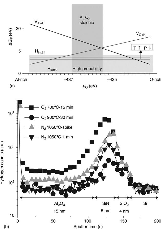
For Hint in position #1, the DOS of its three charge states was computed. As shown in Fig. 4.23, Hint #1 in the neutral charge state (D0) provides two energy levels inside the band gap: one is empty and the other one is occupied by one electron. This was confirmed by the G0W0 calculations (Table 4.1). From this configuration when an electron is introduced in the system (D-) the trap depth is strongly increased and H remains in an interstitial position. When the system loses an electron (D+), Hint #1 is attracted by the negative charge of a nearest-neighbour oxygen and binds to it forming a hydroxyl bond that does not give any level in the band gap. The behaviour of interstitial Hint #2 is different. In this case H is always bonded to its nearest oxygen neighbour with almost the same global configurations for its three charge states. H acts in this case as a shallow donor, as the D0 level lies above the conduction band (Robertson and Peacock 2003). As general conclusions concerning the role of hydrogen are: (i) H does not passivate O vacancies; and (ii) is able to generate stable energy levels inside the c-Al2O3 band gap.

Table 4.1
Synthesis of defects inside c-Al2O3. Defect stability is given by the Gibbs free energy of formation. Activity concerns the potential presence of an energy level in the band gap. Energy level precises the trap depth of the first free level based on DFT/LSDA calculations for D0 state. G0W0 corrections are given for some of the defects
| Parameter | Defects | |||||||||
| VAl | VO | Oint | Alint | AlO | OAl | VAl + H | VO + H | Hint#1 | Hint#2 | |
| Stability | Low | High | Medium | Low | Low | Low | Low | Medium | High | High |
| Active | No | Yes | Yes | Yes | Yes | Yes | No | Yes | Yes | Yes |
| Energy from CB (eV) DFT/LSDA | None | − 0 | 1.1 | None | None | 0.5 | None | None | 0.8 | None |
| Energy from CB (eV) G0W0 | − 0 | 2.1 | ||||||||

To evaluate the role of Al2O3 H-related defects on the retention characteristics of charge-trap memories, the trap parameters coming from atomistic simulations and validated through the fitting of Al2O3 leakage currents were introduced in a complete device physical simulator of TANOS memory (Padovani et al. 2008, 2009). In parallel, a detailed experimental study of retention behaviour was performed on TANOS memory devices, with a 3.5 nm tunnel oxide, 6 nm LPCVD Si3N4 charge trapping layer, 16 nm ALCVD Al2O3 layer – with two different PDAs – and AVD® TaN control gate. Note that, due to the junction anneal, Al2O3 is crystalline at the end of the process whatever the PDA. Figure 4.24 shows the analysis of the impact of the alumina PDA on the retention characteristics. The PDA does not impact retention when the charge loss through the tunnel oxide is dominant (VG = 0 V). On the other hand, when the charge loss through Al2O3 is dominant (VG = 4 V), the 900 °C alumina PDA offers an improved retention behaviour, due to the lowering of the Al2O3 leakage current.

Based on this experimental understanding, the device physical modelling was used to simulate experimental data. Firstly, an accurate reproduction of the program characteristics of TANOS memories with the two different PDAs was created. This gave means to extract the electron distribution in the nitride layer immediately after charge injection (before retention). Then, the retention characteristics were simulated for various applied VG. The simulation was assuming trap assisted currents through Al2O3 with 700 °C and 900 °C PDAs with the same trap parameters as extracted in IV characteristics of Al2O3 single layers. Simulated retention characteristics show a very good agreement with the experimental data (Fig. 4.25). Simulated retention characteristics without traps in Al2O3 were clearly evidence of the role of Al2O3 defects on memory charge loss. In conclusion, the improved retention with the 900 °C Al2O3 PDA is due to the significant H-related defect density decrease and thus decreased alumina leakage.

4.5 Split-gate charge trap memories
4.5.1 Introduction
Split-gate charge trap memories combine a discrete storage layer (to achieve robustness to SILC, scalability, etc.) and a split-gate architecture (to achieve low power consumption, small circuitry, high speed, etc.). Two main approaches exist in the market for microcontroller products: Freescale proposes the ‘Kinetis’ Microcontrollers integrating the ‘Thin Film Storage’ technology (silicon nanocrystals) in the 90 nm (Kang et al. 2012); Renesas put in production in 2007 a silicon nitride charge trapping layer based split gate (Yano 2012) for automotive microcontrollers embedded products. Key advantages of split gate charge trap memories are high program throughput, no over-erase, high reading current and low module area overhead. On the other hand, they have a medium bit cell area, larger than the standard 1T-NOR architecture.
4.5.2 Basics of split-gate charge trap memories
A split-gate charge trap memories with a ‘memory last’ configuration was processed, meaning that the Memory Gate (MG) is deposited on the Select Gate (SG) electrode. Electron beam lithography was used to define control gates down to 40 nm and the channel widths (W) down to 100 nm. The electrical memory gate length is controlled by the poly-Si layer overlapping the memory channel, allowing a gate length down to 20 nm (Fig. 4.26). In the following, LGM will refer to this electrical length. Various gate stacks were integrated with Si-nc (Sample A), Si3N4 (B) and hybrid Si-nc/SiN (C) charge trapping layer CTL (Molas et al. 2007). Finally, Si-nc/SiN CTL was combined to HTO/Al2O3 control dielectrics to allow FN bottom erase (D). Technological details of the various samples are given in Table 4.2.

Table 4.2
Technological details of the studied split-gate charge trap memories
| Sample A | Sample B | Sample C | Sample D | |
| Tunnel oxide | SiO2 (5 nm) | SiO2 (5 nm) | SiO2 (5 nm) | SiO2 (4 nm) |
| Charge trapping layer | Si-ncs (Φ ~ 6 nm) | SiN (6 nm) | Si-ncs + SiN (3 nm) | Si-ncs + SiN (3 nm) |
| Control dielectrics | HTO (8 nm) | HTO (10 nm) | HTO (10 nm) | HTO (3 nm) Al2O3 (8 nm) |
| Control gate | Poly-Si | Poly-Si | Poly-Si | TiN |
The split-gate memories are programmed using Source Side Injection (Van Houdt 1995), biasing both the memory gate and the source electrode at high voltages. The select gate potential is set in order to operate close to the threshold regime (IS ~ 10 μA). Figure 4.27 shows the program characteristics of Si3N4, Si-ncs and hybrid Si-nc/SiN split-gate memories for various programming VMG and VS, and compares their memory windows. Due to a higher density of trapping sites, nitride memories exhibit a higher ΔVT than Si-ncs. The hybrid Si-ncs/SiN layers offer a good way to enlarge the Si-ncs memory window (Molas et al. 2007).

Various erasing modes were used, depending on the nature of the charge trapping layer:
1. nitride based memories are erased using Hot Hole Injection (HHI);
2. Si-nc memories with HTO control dielectrics are erased by Fowler-Nordheim (FN) injection through the top oxide; and
3. Si-nc memories with high-k control dielectrics are erased by FN injection through the bottom oxide.
Figure 4.28 presents the corresponding erasing characteristics; HHI allows faster erasing speed but suffers from a higher current consumption. In FN mode, + 16 V and − 16 V gate voltages are respectively used to erase memory samples with HTO and Al2O3 control dielectrics.
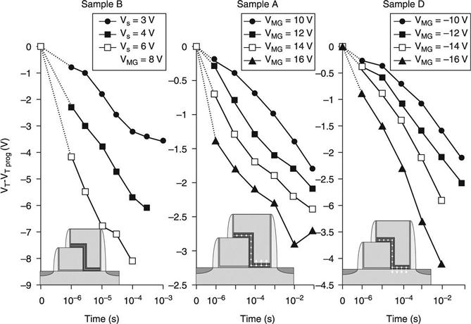
Figure 4.29 presents the retention characteristics. High temperature activation is measured with a nitride CTL with a strong charge loss at 150 °C (Fig. 4.29(a)). While Si-nc/SiN CTL exhibits a more stable behavior as the temperature is increased (Fig. 4.29(b)). Figures 4.29(c and d)) show the comparison of the memory samples at 85 °C and 150 °C. Up to 85 °C, Si3N4 CTL offers the best retention performances. For higher temperatures, an inversion of trend is observed as Si-nc memories present the smallest charge loss. For all the investigated temperatures, memories with high-k control dielectrics show faster charge decay. This is due to the thinner tunnel oxide and the lower barrier height of Al2O3 compared to SiO2.

4.5.3 Scaling of split-gate charge trap memories
Select gate scaling
The effect of the select gate scaling on the programming current consumption was investigated by measuring the select gate threshold voltage lowering and the programming window for devices with a select gate length from 350 nm down to 40 nm. Figure 4.30(a) shows that as the select gate dimensions scale, the memory window remains unchanged but the select gate threshold voltage decreases due to DIBL (drain induced barrier lowering). This parasitic effect causes, for a given VSG, an increase of the consumed current during program operation. For instance, as the select gate scales from 90 nm to 40 nm, a pulse of 10 μs with VS = 3 V; VMG = 10 V; VSG = 1 V (corresponding to the same ΔVT in the two devices (Fig. 4.30(b)), and a current consumption increase of about one decade was measured. Indeed, the DIBL in devices with scaled LSG is a consequence of insufficient control of the channel potential by the select gate. At high applied source voltages this induces, similarly to the case of the strong inversion described above, an increase in the consumed current and a lowering of the electric field that results in a lower injection efficiency (ΔVT/IS). Therefore, in ultra-scaled devices, optimizing the junction implantation and the channel control by the control gate is of great importance to control the consumption. In particular, for the 28 nm node, a high-k metal gate in the access transistor may help in the improvement of the memory performances and consumption reduction.

Memory gate scaling
The impact of memory gate scaling on the current consumption has been investigated. This was done by studying the programming characteristics of devices with a 100 nm select gate length and a memory gate length from 180 nm down to 30 nm (Masoero et al. 2012). Figure 4.31 shows the programming window after a long 500 μs program pulse. With the shrinking of the memory dimensions, the programming window strongly increases from 3 V to 9 V. This result has been explained by means of TCAD simulations.
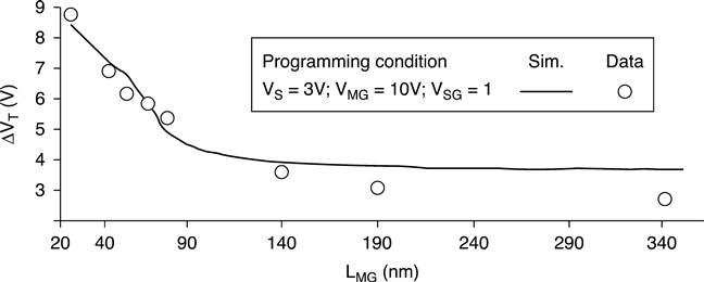
In long devices the electric field in the memory channel shows two peaks (Fig. 4.32(a)): the first peak is located in the gap, due to the difference between the memory gate and the select gate potentials; the second peak is created at the channel source junction. As the gate length is further reduced, the two peaks merge and the maximum of the electric field increases, leading to an enhanced injected charge in the nitride layer (Fig. 4.32(b)). This memory window enhancement in scaled devices can be used to reduce the programming consumption. To analyse this effect, the required programming time to reach a given programming window of 3.5 V and the corresponding energy consumption for various memory gate lengths was extracted. The consumed energy is calculated as the integral along the programming time of the channel current multiplied by the applied source voltage. In scaled devices the memory window is higher but the average current consumed during a programming pulse is nearly constant as it only depends on VSG. The result shows an improvement of over 10 times of consumption energy when the memory length passes from 100 nm to 40 nm. In particular, for sub-90 nm gate length devices, less than 1 nJ of programming energy is reached, suitable for low power applications (Fig. 4.33).


4.6 Conclusion
Two alternative solutions were presented and discussed in this chapter for embedded memory applications: charge trap memories (including nanocrystals and nitride layers) and split gate architectures. These solutions are envisaged to address the two main issues of embedded memories for future generations: reliability and cost.
Silicon nanocrystal memories have shown promising performances. Optimizing the nanocrystal features and the programming schemes good cycling, fast program erase and sufficient retention. New technologies such as metal nanocrystals exhibit strong potentialities for advanced technology nodes, especially due to their large memory window. The only problem is that material developments (passivation) are required to avoid metallic contamination and diffusion, and parasitic oxidation.
On the other hand, nitride based memories present a larger memory window than silicon nanocrystals. They may not inure sufficient retention at high temperatures, especially for the automotive market. The introduction of high-k in the gate stack of charge trap memories can reduce the operating voltages of several volts of the memory device and thus reduce the costs. However, the presence of traps in the high-k layer combined with the intrinsic lower band gap can reduce their insulating capabilities, degrading the retention performances, in particular at high temperatures, and making it critical to optimize the thermal treatments to reduce the trap density as much as possible.
Split gate architecture offers high potentialities for embedded applications, as it is a fast memory with low operating power compared with Flash NOR memory. Scalability of this concept was demonstrated down to 20 nm for the memory gate length. It has an improved programming efficiency and reduced energy consumption suitable for contactless applications. The aggressive scaling of the access transistor and the compatibility with high-k for sub 28 nm node will be the next challenges for this technology.