
Metal oxide resistive random access memory (RRAM) technology
G. Bersuker and D.C. Gilmer, SEMATECH, USA
Abstract:
Detailed operational and intrinsic switching characteristics for hafnia-based resistive random access memory (RRAM) are presented, including materials/vacancy engineering ramifications. The entire set of reported experimental data and material structure modeling and transport simulation results are consistent with the physical picture of the RRAM operations as caused by oxidation/reduction processes in a conducting filament formed in the dielectric. The outcome of the filament formation process establishes initial structural conditions for the subsequent Reset and Set operations. A microscopic description of these processes, the framework of which is presented here, directly links the device electrical and material characteristics, thus enabling improving device performance through optimization of the material compositional profile and operation conditions.
Key words
resistive random access memory (RRAM); ReRAM; memristor; HfO2; hafnia; resistance change
9.1 Introduction
Continued progress in the various types of memory systems, such as high density memory cell arrays, dynamic random access memories (DRAM), NAND, storage class memory (SCM), advanced embedded type applications, etc., depend on continued advances toward low operation current and voltage range while increasing density and speed. In addition, the rising requirements for reducing power consumption for mobile application and convenience of use have increased the efforts and focus toward technology development of non-volatile memories.1 In this respect, the resistance switching random access memory (RRAM) technology presents an attractive option, due to its demonstrated potential for low-complexity/high-density/high-speed/low-cost/low-energy non-volatile operation and prospective ability to satisfy the requirements of many of these advanced scaled memory system types.2,3 Within a large family of the metal-oxide based resistance switching memory schemes, a common characteristic is that their operating mechanisms involve either rearranging of the atomic structure of the dielectric material (rendering it conductive) or movement of atoms in the dielectric (resulting in the formation of a conductive path), as opposed to the current incumbent memory technologies based on the electron storage. The variety of resistive switching memory types currently under consideration are discussed in other chapters of this book, but here we focus on the transition metal-oxide filament-based RRAM, which offers promising opportunities.
The metal-oxide based filament type systems involve repeatable formation and rupture of a localized conductive ‘path’ or filament through the metal-oxide dielectric or resistor, and have the unique attribute of area independent resistance. This attribute suggests an ultimate scaling advantage that is only limited to the active filament size, which potentially may be as small as a few nm. The specific mechanisms in filament-type switching depend on the materials (dielectric and metal electrodes) employed in the fabrication of the memory cell and may involve more than one type of a conduction mode. The filament-based metal-oxide RRAM implemented with a variety of transition-metal-oxides (i.e. HfO2, ZrO2, Ta2O5, TiO2) has received considerable attention due to demonstrated nano-second, low power (< pJ) switching with high (~ Trillion cycle) endurance and retention of more than 10 years at 200 °C, using fab friendly and simple binary oxides and metal electrodes.4–12
Within this group, the HfO2 dielectric, recently becoming mainstream in advanced transistor gate stack application, has also now become one of the stronger candidates for RRAM.6,9,10,13,14 Some of the advantages of HfO2 for metal-oxide filament-based RRAM, besides the proven ‘fab-friendly’ track record, are the extensive research performed from about 1997 to 2007 developing gate-stacks for advanced logic using metal-gate High-K with HfO2 toward manufacturability and productization, assisting the detailed understanding of HfO2 conductivity, and breakdown mechanisms.15–18 In addition, HfO2 has one of the stronger oxygen affinities for transition metals and thus, thermodynamically speaking, is relatively stable and compatible with most of the commonly used fab-friendly electrodes such as TiN, TaN, W, etc.19–24
Despite significant efforts, details of the microscopic mechanisms involved in switching operations in the HfO2-based RRAM still remain unresolved, which is hampering further progress. This chapter focuses on the HfO2-based RRAM system, discussing optimization of the device properties via material engineering and developed atomistic models for possible mechanisms involved in the observed repeatable resistance switching. Some of the processes contributing to resistive switching may be active in other metal-oxide RRAM systems; however, due to the material-specific nature of RRAM characteristics (in particular, relative oxygen affinities, valance states and atom diffusivities), any conclusions or comparisons to other material systems must be made with care.
9.2 Operational characteristics of HfO2-based RRAM
Typically, RRAM systems employ a metal-insulator-metal (MIM) structure for the electrically stimulated change of the resistance, and this configuration is often referred to as a 1-resistor or 1R configuration. The resistance change behavior for bi-polar operation of filament-based RRAM switching, such as observed for HfO2, is shown in Fig. 9.1(a), where an ohmic Low Resistance ‘ON’ state (LRS), or a non-ohmic High Resistance ‘OFF’ state (HRS), can be related to the formed conductive filament (CF) or its rupture, respectively (Fig. 9.1(b)). To describe the material changes in the dielectric associated with this type of resistive switching, we must start with the CF formation, where a microscopic description of the CF features that enable memory operations have only recently been proposed.25

The CF forming process in HfO2 can be discussed in terms of dielectric breakdown (BD), an abrupt formation of a localized region between the electrodes, within which the dielectric composition becomes more oxygen-deficient, rendering this region conductive (the CF formation). The associated abrupt conductance change for this CF formation is observed during the dc voltage sweep or ramp of the RRAM dielectric ‘fresh state’ (Fig. 9.2). This figure also indicates the typical dc switching operation for filament-based RRAM, as noted on the graph with:
1. Forming: a dielectric breakdown event leading to a CF; the voltage of the abrupt breakdown (forming) is termed VF;
2. Reset operation: where the device changes from the LRS to the HRS state due to rupture of the CF; and
3. Set operation: where the device changes from the HRS to the LRS state due to re-formation of the CF path.
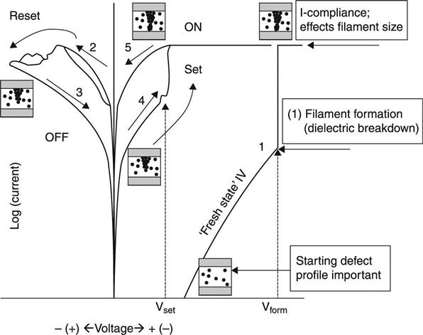
A summary of the typical dc switching operation parameters for the bipolar operated RRAM devices is shown in Plate VI (see color section between pp. 268 and 269). The well-behaved devices can repeatedly switch between the LRS and HRS states for billions of cycles, with the corresponding switching operations being Reset (LRS → HRS), and Set (HRS → LRS), respectively.6,9,14 Note also that ‘anode’ is defined to be the positive voltage electrode and ‘cathode’ defined to be the negative voltage electrode for any applied operational bias. Detailed discussion on the switching mechanisms and modeling of the various switching operations are shown below.
9.2.1 Sources of conductive filament variability
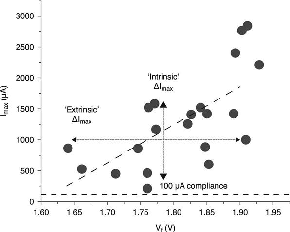
Lack of precise control of the filament formation, perceived to be a random process, introduces variability, both device-to-device (even when fabrication process-related variability can be neglected) and cycle-to-cycle, into the switching characteristics of this class of devices. A reliable figure of merit of the properties of the formed filament (e.g. its size and resistivity) is found to be the maximum current during the first voltage ramped Reset operation after forming (Imax). Devices in which the Imax values are above the compliance current limit (Icomp) used during forming, exhibit lower LRS resistance values (leading to greater power consumption during Reset), and a higher variation in the HRS resistance during subsequent device cycling.26 In extreme cases, the devices with higher Imax vs Icomp can fail to reset. Since a greater Imax likely reflects a larger effective filament cross-section (with lower resistivity) indicative of higher power consumption during memory cell operation, a forming process resulting in lower Imax values is highly desirable.
As illustrated in Fig. 9.3, the device-to-device variation of Imax values can be roughly decomposed into two major contributions: ‘extrinsic’ variation is due to the random distribution of the forming voltage values (Vf) resulting from the voltage ramp forming process, and ‘intrinsic’ variation is due to additional factors determining the conduction characteristics of the filament created at a given Vf. A high Vf distribution strongly correlates to the variability of the subsequent Imax, primarily due to related parasitic capacitance magnifying the released energy at VF (see next section). A constant voltage forming (CVF, which includes also pulse forming) eliminates (by definition) the ‘extrinsic’ Vf distributional variability contribution to Imax, and when performed at low voltages, can also reduce the ‘intrinsic’ contribution. However, only when the parasitic capacitance is substantially small (~ < 100 fF), can the variability from any Vf distribution be eliminated.
9.2.2 Variability caused by compliance current overshoot
Due to excessive parasitic capacitance (Cp) in RRAM devices with external 1T1R circuit or external parametric analyzer used for Icomp, the maximum current through the RRAM device during forming may surpass the current compliance limit, Icomp, set by the transistor (or parametric analyzer) as a result of the AC path arising from the Cp. Imax = Icomp + ICp.26,27 The transient (overshoot) current, ICp, induced by this parasitic capacitance is proportional to dV/dt, the rate of the voltage decrease across the cell during the dielectric breakdown instance (the final, ultra-fast current-runaway forming phase), as given by ICp = Cp•dV/dt. The peak value of ICp is observed to match well to the Imax (Fig. 9.4), indicating that the pre-set compliance limit determined by the external current compliance limiter in series with the RRAM cell is not always effective in controlling the current overshoot, thus introducing an uncontrolled random component in the forming process.

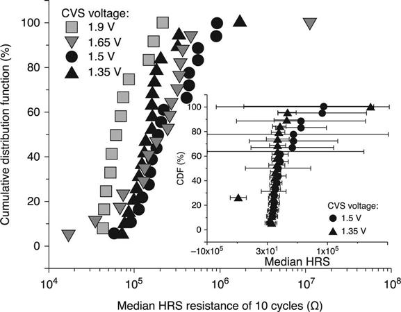
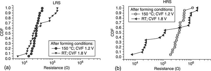
The value of Cp can be reduced through proper device integration (see below), while smaller Vf reduces overshoot (Section 9.3). Suppressing overshoot not only leads to the formation of filaments of smaller cross-sections but also improves LRS and HRS variability (Fig. 9.5) during the subsequent device cycling.26 However, in using the CVF method with a low Vf, the forming process takes too long to be practical for industrial applications. To take advantage of the low-voltage CVF method and its ability to reduce device variability, it was proposed13,26 to perform forming at elevated temperatures that drastically reduces time-to-forming. This ‘hot’ forming method has demonstrated lower LRS and HRS variability and greater memory-windows in subsequent room-temperature switching operations (Figs 9.6(a and b)). The switching mechanism with respect to ‘hot’ forming is discussed in further detail in Section 9.3 below.
9.2.3 1T1R test vehicle
An imbedded (integrated) transistor in series with the memory cell (integrated 1T1R) can better control the current passing through the cell during the filament forming step (and Set operations). When employing appropriately-designed integrated 1T1R structures, the parasitic capacitance can be expected to be less than approximately 50 to 100 fF, which greatly improves current compliance control and minimizes or eliminates overshoot current issues.6,7,28 In addition, when using an integrated transistor to accurately control the filament formation and Set operations (dielectric breakdowns), the intrinsic properties of the RRAM devices can more clearly be revealed. The parasitic capacitance is limited in general by using a smaller area drain, smaller area bottom and top electrodes of the RRAM element, smaller area probe pads and thicker isolation layers. Through use of a specially designed test structure (Fig. 9.7), which allows for testing of the same RRAM element with various configurations of integrated 1T1R, an external parametric analyzer or an external transistor to limit operation current, clearly demonstrates that only the integrated 1T1R substantially minimizes the parasitic capacitance (as manifested by elimination of the Imax current overshoot above Icomp).7
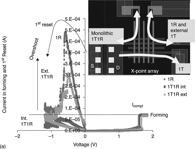
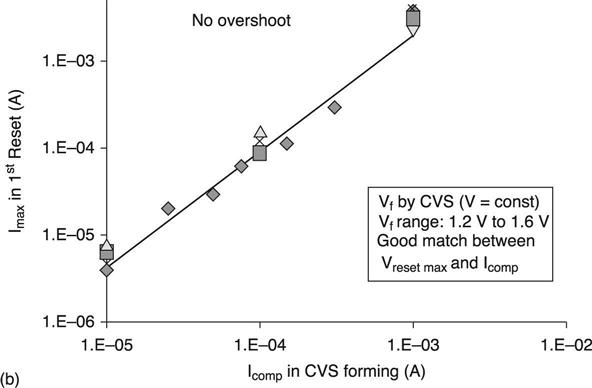
(b) The correlation between the maximum reset current and current compliance values used in the constant voltage stress forming in the integrated transistor case. A linear correlation demonstrates effectiveness of the integrated 1T1R configuration in controlling current overshoot. The experimental set-up for dc and real-time ac characterization are discussed in references 6 and 7.
9.3 Modeling forming and switching processes
9.3.1 Properties of HfO2-based dielectric assisting filament formation
The properties of the initial conductive filament created by the forming process essentially determine the device switching characteristics and therefore we start by considering the forming process. The forming process involves applying a sufficient bias across a dielectric resulting in the formation of a conductive filament, which generally exhibits Ohmic or near-Ohmic type conduction (as follows from observed linear I-V dependency and increasing resistance with temperature). These metallic characteristics indicate that the filament is represented by the Hf rich/oxygen deficient region in the dielectric. Thus, the filament formation is associated with the process of oxygen expulsion from this dielectric region, which is the focus of the following discussion.
We start by identifying the morphological properties of the HfO2 film assisting formation of the conductive filament. For this task, conductive atomic force microscopy (C-AFM) was found to be an effective technique,29–31 allowing a nanometer-resolved characterization of the electrical and topographical properties of the gate oxides.32 When the C-AFM tip-sample system is biased, a current flows through the structure so that along with the surface topographical features the electrical properties of devices can distinguish individual nano-crystals and allow profiling of much of the current both along and across the grain boundary (GB) (depression in the topographical profile). Results demonstrate that the current through the crystalline dielectric preferably flows along the grain boundaries (color Plate VII), consistent with scanning tunneling microscopy (STM) measurements.33 Dielectric breakdown induced by the continuously applied voltage also preferentially occurs at the GB sites.
Ab initio calculations of the GB structures in monoclinic HfO2 were employed to identify the GB properties responsible for the current flow. Despite the boundary stability, segregation of vacancies to the boundary is thermodynamically favourable.34 The formation energy and properties of vacancies segregated to the boundary are modified as their concentration increases. Neutral O-vacancies (Vo) can achieve spacing at the GB down to about 3.5A, while positively charged vacancies (V+) can be placed with spacing as close as about 5A.
At the low vacancy concentration, individual defect states are introduced into the HfO2 band gap. Higher vacancy density at GB leads to the creation of a conductive sub-band confined to the GB region due to overlapping of the localized Hf d-states in the HfO2 band gap. This sub-band effectively constitutes a percolation path for the current flow, in agreement with the C-AFM and STM results, which show a perfect match between the maps of the leakage current and GBs.
9.3.2 The role of grain boundaries
Electrical transport along the GBs can be successfully described by the multi-phonon trap assisted tunneling (TAT)35 via the vacancy sites. The leakage current through the TiN/HfO2/TiN capacitor was simulated,36,37 considering both direct tunneling (DT) and TAT components of the gate current. The TAT current, which is shown to be the dominant component in the substoichiometric hafnia discussed here, is calculated by taking into account contributions from the single-trap and multi-trap conductive paths by the defects randomly placed along the GBs. The current driven through a conductive path, I, is determined by the slowest trap in the path as
[9.1]
where e is the electron charge, and τc and τe are the time constants associated with the electron capture and emission, respectively, by the slowest trap. The calculations of τc(e) take into account the electron tunneling to/from the oxide trap and lattice relaxation associated with the electron trapping/detrapping,38–40 which causes displacements of the oxide atoms due to the Coulomb attraction between their nuclei and the electron. While the tunneling portion of the charge transport process is temperature independent, the lattice relation governed by the electron-phonon interaction generally strongly depends on temperature. This relaxation introduces a barrier to the electron trapping process which, within the high temperature approximation, can be approximately described as exp (− Eb/kT), where the effective barrier is expressed by
[9.2]
Here EF is the electrode Fermi level and Et and Er are trap total energy and its relaxation energy, respectively. These trap characteristics, which identify the trap atomic structure and its charge state, can be extracted by matching voltage/temperature dependencies of the calculated and experimental currents.
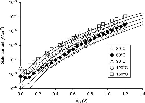
The TAT description successfully reproduces current-voltage (I-V) temperature dependency in the crystalline hafnia (Fig. 9.8).41 The extracted values for the energy of the contributing traps and their relaxation energy match those calculated for the V+ at the GBs,34 indicating that the TAT current is associated with the (V+ + e → V0 → V+ + e) process. Since the doubly positively charged O-vacancies [V(2 +)], which can be present in hafnia, exhibit lowest diffusion activation energy (0.6–0.7 eV),16,34 their eventual segragation at the GBs leads to the formation of a conductive sub-band within the dielectric energy gap. By capturing the injected electrons, these vacancies are converted to a V+ state, which is shown to support the TAT current. As discussed below, a current flow along the GBs facilitates dielectric breakdown at these locations, which results in the preferential formation of the conductive filaments at the GBs in metal oxides.
To evaluate the effect of GBs on the memory cell characteristics, the forming/switching operations were performed in nano-scale by using the tip of a C-AFM probe as a top electrode of the MIM memory device (the biased substrate constitutes the bottom electrode).29 As seen in Fig. 9.9, higher conductivity of the GBs in the polycrystalline film is accompanied by lower forming (breakdown) voltages. These low forming voltage sites at GBs exhibit repeatable resistive switching, while no switching is observed when the forming is induced on the grain sites (as well as in the case of an amorphous stoichiometric HfO2), which exhibit significantly higher forming voltage values. These results indicate that resistive switching is benefited from higher oxygen deficiency of the dielectric that makes it less resistive and reduces the forming voltage. Indeed, devices fabricated using the stack of a HfO2 dielectric and overlaying thin metal film that scavenges or ‘getters’ oxygen from HfO2 leading to the dielectric oxygen deficiency as shown by the synchrotron XPS data (Fig. 9.10), demonstrate much better switching characteristics than those of lower oxygen deficiency (the gettering metal can be an early transitional metal (i.e. Ti, Zr, Hf, etc.)). These gettering metal layers are often termed oxygen exchange layers (OEL) in RRAM stacks, even though any oxygen exchange may not be reversible.


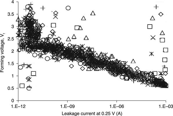
Limited spatial resolution of the available physical characterization techniques does not allow addressing the relationship between the oxygen gettering process and film morphology, although physical observations combined with electrical data have implicated HfO2 GBs as susceptible toward reduction, even when not favored from bulk thermodynamic considerations.42 However, certain aspects of the gettering process can be deduced directly from electrical measurement data, in particular from a trend between the leakage in fresh devices and their forming voltages, which is observed in devices of different areas and various combinations of oxide and metal-OEL thicknesses (Fig. 9.11).43 To explain such trends, we may consider that the oxygen scavenging proceeds more effectively along the GBs where the bonding of oxygen is known to be weaker34 and the oxygen ion diffusion rate is higher.44 The oxygen extraction from GBs is expected to occur essentially non-uniformly, with oxygen being more efficiently scavenged from the GB portion located in closer proximity to the metal layer. As a result, a GB portion next to the metal film is less resistive (due to higher concentration of the oxygen vacancies there), while a more stoichiometric section of the GB constitutes an HfO2 dielectric barrier, albeit with higher density of oxygen vacancies than that of the regular, ‘un-gettered’ oxide (Fig. 9.12).

Such stochastic process of oxygen gettering is expected to proceed differently in each GB due to variability of the GB characteristics (orientation, length, structure, etc.), resulting in a distribution of thicknesses of the dielectric barriers in the various GBs of each given device and, subsequently, a distribution of the magnitudes of leakage currents through these various GBs. The GB where the oxygen extraction was the most efficient (for whatever reasons) represents the preferential conductive path through the HfOx film. The leakiest path is expected to have the thinnest barrier since the electron transport through the barrier controls the overall current. This thinnest barrier should be the first one (out of all the barriers in other less conductive paths) to be broken by the applied voltage during forming. Thus, a single structural feature – the thinnest GB barrier in a given device – is responsible for both the lowest breakdown voltage magnitude (that is the forming voltage) and highest leakage current (which is proportional to the total current through the device43) that explains their correlation.
This hypothesis was tested by modeling the leakage current and forming voltage (using the multi-phonon TAT description), which was calibrated by matching the I-V dependencies in a variety of HfO2 devices in a wide range of temperatures, from 6 to 400 K,45 with different ratios of the metal/dielectric thicknesses. The observed I-Vf trend for different ratios is successfully reproduced by varying the barrier thickness and densities of vacancies, which support the current through these barriers (Fig. 9.13). The simulations show that devices with higher ratios of the metal to oxide layer thicknesses have thinner barriers with slightly higher vacancy densities, as expected. Thus, one of the beneficial effects of oxygen gettering is a creation of highly conductive current paths, which exhibit low forming voltages – consistent with the above discussed C-AFM results. However, the major effect is that the dielectric oxygen deficiency enables resistive switching phenomenon, as discussed below.

9.3.3 Mechanism of forming process
We can now discuss the forming process based on the above outlined structural and morphological dielectric features controlling the leakage current in the MIM stack. The forming process in HfO2 can be considered in terms of dielectric breakdown (BD), an abrupt formation of a conductive path between the electrodes. Dielectric breakdown represents a ‘weak link’ event, the occurrence of which is determined by the moment when the first conductive path is formed; therefore, its characteristics are expected to follow the Weibull statistics,46 as is confirmed below.
Bond breakage
As a first step of the formation of an intrinsic conductive path in the dielectric material (without considering infusion of metal atoms from the electrodes), the oxygen-metal bonds have to be broken, which can be described by the Arrhenius dependency:
[9.3]
Here G is the probability of the bond breakage at a given location (x,y,z) in a given moment, and G0 is the characteristic vibration frequency of the Hf-O bond. The barrier (EA), corresponding to the breakage of the Hf-O bond, is lowered by βΕox (x,y,z), due to the polarization of the chemical bonds (as accounted for by β) by the applied field Eox(x,y,z).15,18 Elevated temperatures intensify the Hf-O bond vibrations, increasing the probability of bond breakage. As follows, the effective barrier for dissociation of an Hf-O bond at a given site can be further reduced due to both enhancement of the local electric field and higher local temperature caused by the defect generation and associated electron transport through the generated new defects in the surrounding dielectric region.
Within the TAT description, as discussed above, the current through the dielectric is associated with the injected electrons hopping between the vacancies. The process of the electron localization/delocalization at a vacancy site during the hopping is accompanied by the displacements of the surrounding lattice atoms (the lattice relaxation).40 Thus, each electron trapping/detrapping event is accompanied by the energy dissipation (P), in the form of phonons, around the trap location: P = I/e m ħω0, where I/e is the carrier flux through the trap (Eq. 9.1) and m is the net number of phonons of the frequency ω0 emitted during the charge transfer. This energy dissipation leads to a temperature increase in the surrounding region, a value of which at each (x,y,z) location is determined by the distance from the charge transporting defect, thermal conductivity of materials constituting the device, as well as overall device dimensions and geometry (which determine the boundary conditions):
[9.4]
where kT is the oxide thermal conductivity.
The presence of oxygen vacancies changes locally the dielectric constant, thus affecting the electric field distribution. Therefore, at any moment t, the field and temperature at a given location depend on the spatial distribution of the defects in the entire surrounding dielectric region, n(x′,y′,z′,t), generated prior to this moment in time, t:
[9.5]
where fE(T){n(x,y,z,t)} describes the functional dependency on the defect distribution, which cannot be generally expressed in a compact form (the Eox and T maps can be obtained by numerically solving Poisson, charged carrier transport and heat flow equations for a given vacancy distribution n(x,y,x,t)). Substituting Eq. 9.5 into Eq. 9.3, we see that the local bond breakage rate depends on a global spatial defect distribution that makes G essentially time dependent:
[9.6]
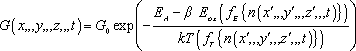 [9.6]
[9.6]
while the defect generation at each location (x,y,z) depends on the overall evolution of the generation rate G(x,y,z,t) over time at this location:
[9.7]
As follows from Eq. 9.6, the probability to generate new defects in the vicinity of the existing one is higher than that at a random location, and it is growing with the density of the defects in the surrounding region (since both Eox and T increase with n(x,y,z,t)). At a certain moment, t0, when a critical number of defects are generated close to each other (forming an oxygen vacancy cluster), the local field-induced barrier lowering βEox (x,y,z,t0) becomes compatible to the bond strength EA, while T(x,y,z,t0) also increases due to a higher charge transport rate through this defect cluster.41 Under these conditions, the defect generation probability Eq. 9.6 increases sharply, triggering a positive feedback process of self-accelerated bond breakage described by the set of coupled Eqs 9.6 and 9.7.
The breakage of additional Hf-O bonds leads to creation of additional oxygen vacancies supporting the electron hopping, which further increases the electron transport through this dielectric region. Higher local current density increases temperature in the surrounding region, promoting generation of new defects nearby. At the same time, formation of lower resistance regions along the conductive path, due to higher local density of the generated vacancies, causes a greater share of the applied voltage to drop across the dielectric regions of higher resistance41 which, in turn, enhances the vacancy generation rate there. This temperature-field driven process of vacancy generation in the vicinity of a critical size defect cluster describes a runaway dielectric breakdown.
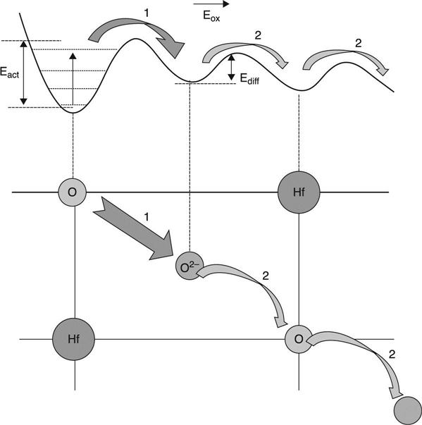
Upon breakage of the Hf-O bond, some of the oxygen ions diffuse out of the high current region following the temperature/density gradient, while others may recombine with the nearby vacancies and become subject to the possible subsequent bond breakage events. The oxygen release and its out-diffusion culminate in the formation of the oxygen deficient (hence metal (Hf)-rich) region through the dielectric, called the conductive filament (CF). Formation of a conductive filament, which is accompanied by a change of the charge transport mechanism, constitutes a forming event observed in electrical measurements, as an abrupt current increase by up to several orders of magnitude.
The model suggests that the CF resulting from the above-described temperature-field driven forming process might be of a cone-like shape. Indeed, more energy is dissipated during each electron trapping event when it occurs at the traps located further away from the cathode due to acceleration of the injected electron by the applied electric field. In addition, the charge transfer rate (the characteristic times in Eq. 9.1) of the positively charged vacancies located further away from the cathode is also higher, because of their lower trapping barrier (Eq. 9.2), due to relatively high relaxation energy of these defects. Higher power dissipation, in turn, translates to higher rates of oxygen dissociation and out-diffusion in farther proximity from the cathode, which facilitates the formation of a wider oxygen deficient area. The TEM-EELS data are consistent with the proposed cone-like shape of the filament (color Plate VIII between pages 268 and 269),47 the filament cross-section being observed to be larger with higher forming current compliance, in accord with electrical data.25
Formation of vacancy cluster
The bond breakage discussed above represents the initial step in the CF formation process. The final CF characteristics depend on the diffusion of the released oxygen ions, and their spatial distribution in the dielectric at the end of the forming process, thus directly affecting the subsequently performed reset process. Obtaining this CF information requires detailed description of the kinetics of oxygen release and its diffusion during forming.
Filament formation starts from the initial ‘preferred’ conductive path along the GB, as described above. When the Hf-O bonds ‘break’, the O(2 −) ion shifts to the interstitial lattice position leaving behind a double positively charged vacancy, V(2 +). Due to a strong Coulomb coupling in the V(2 +)-O(2 −) pair (Frenkel pair), the ion-vacancy separation requires a sufficiently high electric field in the oxide, unless the positive charge is instantaneously compensated for by a capture of an injected electron (a relatively low probability event). However, this process can proceed more efficiently when the Frenkel pair is created next to the already negatively charged vacancy with two captured electrons (such vacancy charge is feasible under the high electron flux conditions), which can transfer to the newly formed vacancy and compensate its positive charge.48
The situation changes when a cluster of overlapping vacancies is eventually formed. The injected electrons captured by such a cluster are delocalized through the entire cluster volume and fully compensate positive charges associated with the oxygen vacancies. When a new vacancy is created at the interface between the metal-rich cluster and surrounding oxide, the vacancy charge is instantaneously neutralized by the electrons shared within a cluster. This significantly reduces the activation energy for releasing the O(2 −) ion as compared to the formation of an isolated vacancy in the bulk of HfO2.49 The cause of this lower activation energy is the absence of an electrostatic coupling between the O(2 −) ion and the neutral cluster. Thus, formation of an initial vacancy cluster reduces the energy penalty for oxygen ion out-diffusion and assists the cluster growth process described by Eqs 9.6 and 9.7.
Under a sufficiently high compliance current limit, the vacancy cluster grows and eventually creates a continuous conductive filament through the entire dielectric thickness, which is usually manifested electrically by Ohmic-type conductivity. As follows from the above discussion, filament growth during the runaway phase of the forming process should proceed preferentially via the oxygen ion release from the filament outer surface (Fig. 9.14). Formation of the initial vacancy cluster comprises most of the time required to form a conductive filament (to reach a dielectric breakdown41) under given conditions; when a cluster of a certain critical size is created,49 its continued growth is expected to proceed at a very high rate.

According to ab initio calculations,17,50 the released interstitial O(2 −) ions in HfO2 diffuse (by substituting the regular oxygen atoms) with the activation energy of Ed = 0.7 V. The O(2 −) diffusion can be described as proceeded via an O(2 −) ion hopping between unoccupied interstitial positions with the rate:
[9.8]
where Ediff(x,y,z,t) = Ed – Q* λ/2*Eox(x,y,z,t), λ is the hopping distance (~ O-O distance), Q is the ion charge, and ν is the characteristic vibration frequency (Fig. 9.15). In addition to the applied field, the local field Eox(x,y,z,t) also includes the ion-ion and ion-vacancy Coulomb repulsion and attraction components, respectively, which depend on the spatial distributions of the O(2 −) ions and vacancies (some of which are confined within the grain boundaries) at any given moment, t.
Forming process simulations
The forming process can be approximated by two phases:
1. an initial stage dominated by the trap assisted tunneling conduction via pre-existing vacancies, which is characterized by limited vacancy generation;51 and
2. the final, sub-nanosecond, thermal-runaway phase, when vacancy-generation proceeds effectively via a self-accelerated (positive-feedback) process.41
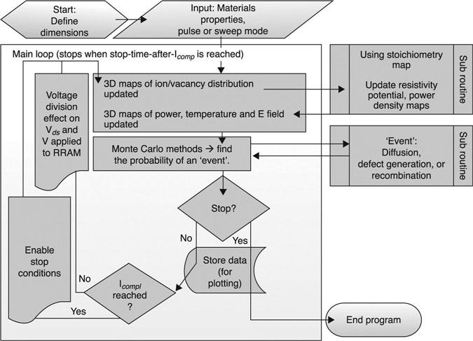
The discussion now focuses on the second, fast phase. The bond breakage and oxygen diffusion processes cannot be described in a closed analytical form because of their probabilistic nature and essentially non-local characteristics (Eqs 9.6 to 9.8) and therefore require the use of Monte Carlo simulations based of the rate equations.41,51,52 The simulations start with constructing a unit memory cell containing the multilayer stack of metal electrodes, OEL and dielectric materials. The metal oxide dielectric layer (in this case, HfO2) is initially randomly seeded with the carrier transporting defects (oxygen vacancies) distributed across the dielectric thickness and confined to the regions representing the grain boundaries (their radius is calculated to be ~ 0.5 nm).34 The initial non-uniform vacancy distribution should reflect on the conditions expected in the result of the OEL layer gettering of O ions from the initial HfO2 material: vacancies are preferentially located in the grain boundaries,34,43 closer to the metal OEL layer.
In the final runaway phase, which is characterized by the high density of vacancies within a conductive path where the TAT description of the charge transport is no longer valid, we consider the electron drift through a defect sub-band. Such electron drift or transport can be described by the effective resistance approach,52,53 when every elementary volume (bin) of the discretized dielectric space is assigned with an effective resistivity value, which depends on the oxygen vacancy concentration in this bin. At each iteration corresponding to a certain time interval, the program calculates the voltage across the RRAM (VRRAM) taking into account the effective load resistor (RLoad), and then current and corresponding 3D local electric field and temperature maps at each elementary bin (Fig. 9.16). Next, the probabilities of the vacancy generation (oxygen displacement to an interstitial position) and oxygen hopping (for the already shifted oxygen) are calculated for each oxygen ion throughout the entire volume. After each vacancy generation or ion-vacancy recombination event, the change in stoichiometry is translated into the change in the local resistivity of the corresponding bin, based on which a new field and temperature distribution is recalculated. The 3D maps of vacancy positions, ion positions, temperature, resistivity, electric field and I-V curve data are generated at each iteration cycle.
Upon formation of a conductive filament (the characteristics of which, specifically cross-section,25 depend on the current compliance limit), the resistance of the MIM device reduces usually by several orders of magnitude and, correspondingly, most of the applied voltage now drops over the external resistance. The measured time for this voltage to change from low to high values defines an upper time length limit of the runaway phase of the forming process, which is experimentally estimated to be less than 3 ns (Fig. 9.17) (limited by the measurement set-up resolution).52 The runaway time period, during which most of the oxygen ions are released, determines the duration of the directional ions diffusion under the influence of an applied field Eox.

By reducing the effective diffusion barrier, the applied field during forming directs oxygen ions towards the anode electrode. Oxygen ions, which reach the metal layer (OEL) at the oxide/anode interface, oxidize it54 and, therefore, cannot readily be extracted back to the conductive filament and contribute to the subsequent Reset process when an opposite bias (of a relatively small amplitude on the order of 1 V) is applied. However, the Coulomb repulsion between the oxygen ions slows down their transport along the direction of the external field, and a significant number of ions do not reach the metal layer during a very short transient (runaway) forming phase. These ions remain in the filament vicinity (in the interstitial positions), as illustrated in the example of a voltage ramp forming simulation (color Plate IX in colour section between pages 268 and 269) and are available for a subsequent Reset operation as discussed below. In a radial direction, the released ions move along the density/temperature gradient, their diffusion slowing down as the temperature decreases with larger distance from the filament.
According to the simulation results, higher forming voltages Vf increase the defect generation rate, which depends exponentially on the local electric field in the dielectric (Eq. 9.3), leading to shorter forming transient times (and potentially greater overshoot). By comparing radial and vertical distributions of the generated vacancies and diffused ions immediately after completion of the runaway phase, we find that under a higher forming voltage condition the oxygen ion and vacancy distributions significantly overlap (color Plate X(a′)) indicating limited O(2 −) diffusion. This is strikingly different from the low forming voltage case (color Plate X(b′)), which exhibits a more spread-out radial distribution of the O(2 −) ions due to a much longer duration of the transient (runaway) phase. Simulations show that during the transient (runaway) phase, variations in the filament geometry caused by random vacancy generation at multiple sites along the conductive path induce local spikes in the electric field. These spikes reduce the effective activation energy for vacancy generation (Eq. 9.3), causing its rates to be higher than those of ion diffusion and recombination. Therefore, when the forming runaway phase is shorter, as in the higher voltage case, oxygen ions generated at a high rate do not have time to diffuse away from the filament. The use of higher ambient temperature accelerates the onset of the runaway phase in the trap generation process, thus enabling forming at lower voltage conditions to occur within a practically reasonable timescale.
The diffusion and recombination processes continue after the transient phase, when the forming current compliance limit is reached and the voltage across the device sharply decreases; it drops instead across an external resistance, while the current continues to flow at the compliance level. During this ‘relaxation’ period (of no vacancy generation, but still higher temperature around the filament), more recombination events occur in the higher voltage forming case, since more ions are located in close proximity to the filament at the end of the vacancy generation period (Plate X(a′)). A lower forming voltage results in greater radial distribution or spread-out of oxygen ions during the relaxation phase. As a consequence, with higher forming voltages (at similar Icomp), the resulting filaments tend to exhibit higher resistance and are less stable (Plate XI(b)).
Switching operations
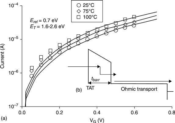
Transition to the HRS by applying a Reset voltage, where polarity is opposite to that of the forming voltage in bi-polar operations, is caused by a rupture of the conductive filament established during forming. To understand the major factors controlling HRS properties, we simulated the HRS currents and I-V temperature dependency for different Reset conditions using the above-described multi-phonon TAT method. The HRS experimental data are reliably reproduced when we assume the existence of an approximate 1 nm dielectric barrier along the CF; the electron transport through this barrier, which includes both direct tunneling and TAT via the traps in the barrier, determines the HRS current.55 As was reported,56 larger Reset voltages result in higher HRS resistance, which is modeled as increased thickness of the dielectric barrier, up to 2.5 nm in the case of a slow dc Reset,57 its band offset and k value matching those of HfO2. The temperature dependency of the HRS current is controlled by the TAT process via defects (oxygen vacancies) in the barrier layer (Fig. 9.18), which density, 2 × 1021 cm− 3, is independent from the barrier thickness. The ionization energy of the contributing traps exhibits a wide distribution, 1.7 to 2.7 eV, matching the values obtained for the electrically active traps, which control the current in a fresh HfO2.41 Therefore, it is reasonable to suggest that the CF rupture is associated with the re-oxidation of a portion of the filament.55 This can be achieved as the oxygen ions, which are out-diffused from the CF region during the forming, move back to the CF when the voltage polarity changes during Reset operation.
Indeed, under the Reset bias, oxygen ions are expected to accumulate near the bottom electrode, which should present a good oxygen diffusion barrier to avoid the irreversible loss of oxygen during repeated switching cycles. In this respect, the TiN electrode appears to meet this requirement for HfO2 RRAM dielectrics: according to ab initio calculation,49 its crystal structure (ignoring its process-dependent polycrystallinity) does not have room to accommodate oxygen atoms, assuming the absence of N vacancies in TiN, and its free energy of oxide formation is much less favored compared to Hf. With sufficiently high density of O(2 −) ions next to the bottom electrode, they tend to diffuse towards the filament, enabled by local temperature and driven by a density gradient and mutual Coulomb repulsion (color Plate XI). It is considered that the affinity of Hf and O-ions lowers the energy barrier for the O-ions hopping into the vacant site in the filament region. The filament works as an oxygen sink: oxygen ions readily bond to the available Hf atoms, thus creating room for the next oxygen ion to move towards the filament. However, ion diffusion in the direction away from the filament is suppressed due to a steep temperature reduction gradient: the lower temperature away from the filament reduces the ion diffusion rate (Eq. 9.8), which in turn slows down further out-diffusion of ions located closer to the filament due to ions’ mutual repulsion.
Therefore, the spatial distribution of oxygen ions at the end of the forming process presents the initial boundary condition for modeling the Reset process. This distribution, achieved under the forming conditions when the temperature at any given site in the oxide is much higher than that achieved during Reset, determines the ‘supply’ region, from which the O-ions might be driven back to the CF during the Reset operation.
Due to a very low O(2–) hopping barrier (0.7 eV), oxygen ion diffusion proceeds very effectively at room temperature, which would lead to an eventual uniform distribution of oxygen ions throughout the entire dielectric volume. This would result in oxygen-depletion of the dielectric region around the filament, thus disabling the reset process (color Plate XII). However, we have to consider that the dielectric film generally contains a significant number of imperfections, specifically grain boundaries in the case of poly-crystalline hafnia, which are known to accumulate oxygen vacancies in a positively charged state, as discussed above.25 These pinned positive charges, the density of which is dramatically increased as a result of oxygen gettering43 (Fig. 9.12), attract negatively charged oxygen ions, preventing them from leaving the CF region surrounded by randomly distributed grain boundaries.58 The energy barrier associated with the vacancy segregation at GBs34 prevents the recombination of the coupled (via Coulomb interaction) oxygen ions and pinned vacancies. These coupled oxygen ions remain within the limited region defined by the grains surrounding the conductive filament (which itself encompasses the GB) (color Plate XII(d′)), thus enabling the high endurance of the HfO2-based devices. The simulations confirmed that the pinned vacancies, with a density determined by the degree of the hafnia oxygen deficiency, can effectively contain oxygen ions enabling repeatable Set/Reset operations52,59 (color Plate XIII).
As seen in color Plate XIII, the simulations demonstrate that a longer Reset pulse (as well as higher Reset voltage)59 leads to re-oxidation of a larger section of the CF, resulting in a less conductive HRS, consistent with the literature reports on the voltage vs time trade-off.60
A switching from high to low resistive state (i.e. Set operation toward LRS defined by the current compliance level) leads to the initial conductive filament being restored. For this, the thin dielectric barrier formed during Reset needs to be broken. Due to relatively high conductivity of the undisrupted portion of the ‘conductive’ filament, most of the applied voltage during a Set operation drops across the dielectric barrier. If this voltage (in particular, a pulse amplitude) is sufficiently high so that the electric field in this thin dielectric layer approaches the intrinsic dielectric strength of HfO2 (estimated to be ~ 4 MV/cm),18 the Hf-O bond breakage proceeds rapidly, resulting in a release of the oxygen ions and restoration of the conductive filament toward its post-forming shape. The description of the Set process (which occurs generally at lower voltages than forming), essentially follows that of the forming process, as discussed in Section 9.3 above.59
9.4 Materials development: engineering vacancy profiles for RRAM
9.4.1 Vacancy assymetry and the filament-based RRAM model
As described in Section 9.3, oxygen vacancies in sub-stoichiometric films may agglomerate (in poly-crystalline film), by accumulating along the grain boundaries,55 thus forming conductive paths through the dielectric. The presence of conductive paths assists with lowering the filament forming voltage, allowing for more controlled conductive filament (CF) formation. The non-uniform cross-section of the CF provides certain advantages for switching operations, with bipolar Reset described as oxidation of the narrower end of the CF tip to form a thin dielectric barrier near the Reset-anode, which for bipolar operation is also near the forming-cathode, leading to the HRS. The subsequent Set operation (from HRS to LRS) is then the breakdown of this thin dielectric barrier, thus reforming the CF. In order for a device to demonstrate well-behaved RRAM switching, the forming and switching conditions should be selected according to the filament composition profile to achieve favorable post-forming distribution of the oxygen ions, which subsequently contribute to re-oxidation of the filament during Reset.
The dc Reset process in an HfOx-based RRAM device (the atomic-level simulations of which are presented above) is illustrated in Fig. 9.19.55 Changes in the LRS during increasing Reset bias are first observed as a deviation of the I-V curve linearity expected for the ohmic LRS due to temperature increase of the CF caused by joule heating (Fig. 9.19 inset shows simulated temperature increase with increasing bias). Eventually, upon continued bias increase and sufficient heat, oxidation of the CF tip begins, as observed by a ‘noisy’ decrease in current with continued voltage increase. This fluctuating resistance manifests the competing with processes of CF oxidation and generation of new oxygen-vacancy pairs in the electrically stressed dielectric barrier, which is growing during the Reset. This model of a Reset process suggests that the vacancy concentration profile asymmetry in the RRAM dielectric stack is critically important for repeatable switching,61,62 as discussed below.

Robust switching in the transition metal oxides (TMO) RRAM devices are known to require some amount of oxygen deficiency of the dielectric film.27,62 It has also been demonstrated that performance of RRAM devices is improved by utilizing asymmetrical vacancy profiles of sub-stoichiometric TMO films. These asymmetrical vacancy profiles are typically formed using reactive-PVD,11,27,63 or through depositing a dielectric or metal and applying a subsequent post-treatment reduction or oxidation anneal,64–66 or with depositing reactive gettering type metals (often termed oxygen exchange layers (OEL) in RRAM stacks) on to the TMO.9,10,14,67,68 Many of the various TMO-RRAM reports in the literature also consistently show bipolar operations with the Reset bias applied having the Reset-anode against the more oxygen rich or more stoichiometric part of the fabricated dielectric stacks.9,10,27,62,63,65–67 The reason the bipolar operation for TMO filament-type RRAM consistently has this polarity preference characteristic is related to the TMO asymmetric defect/vacancy profile, the CF asymmetry and switching mechanism described in Section 9.3. Having less defects/vacancies near the ‘Reset-anode’ allows for a more effective re-oxidation of the narrow conductive filament tip in this region. When an opposite bipolar operational polarity is used to switch the RRAM device, too many defects/vacancies near the ‘Reset-anode’ can prevent effective oxidation of the CF tip.62
9.4.2 Switching in asymmetric vacancy engineered RRAM
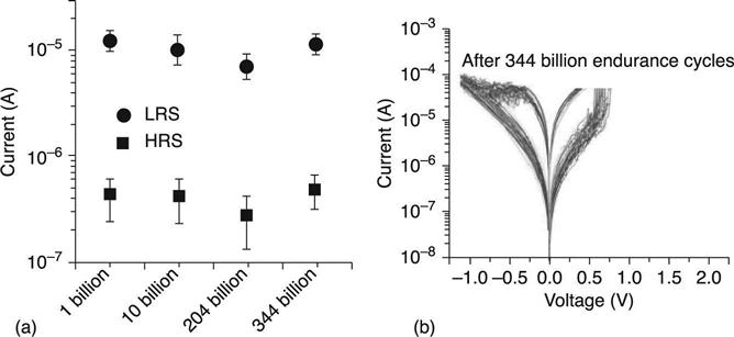
To further investigate the preferred bipolar operational biasing and vacancy asymmetry relationship, various sub-stoichiometric HfOx films with asymmetrical oxygen vacancy profiles were formed.62 A thin OEL of titanium was deposited on top of HfO2 and subsequently capped with TiN, creating an asymmetrical defect/vacancy profile with more defects/vacancies near the OEL side of the stack due to preferential gettering of oxygen from the HfO2 grains and grain boundaries nearer the OEL metal. Figures 9.20(a,b) present the switching behavior for the two possible bipolar biasing schemes (Fig. 9.20(a)) having Reset-anode opposite the OEL (or more defects/vacancies) side, and Fig. 9.20(b) biased with Reset-anode at the OEL (or more defects/vacancies) side). Operating in the bipolar mode with a bias polarity having the Reset-anode against the more stoichiometric part of the film (away from the OEL) results in well-behaved RRAM switching with well over 100 billion ac cycles demonstrated on dimensions down to 50 nm × 50 nm (Fig. 9.21). Operating the device opposite this preferred polarity often results in the failure to reset toward higher resistance states (Fig 9.20(b)), due to difficulty in re-oxidation of the CF because of the high defect/vacancy density near the Reset-anode in this ‘non-preferred’ biasing case.
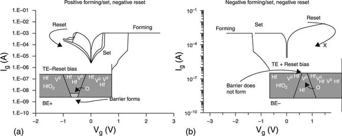
This oxygen vacancy asymmetry and preferred bi-polar biasing is demonstrated further with a RRAM device using a highly asymmetrical HfOx film formed by oxidizing the top of an exceedingly sub-stoichiometric HfOx film. The backside-SIMS profile of the oxygen concentration for this type of stack is shown in Fig. 9.22, indicating the film has high defect/vacancy concentration near the bottom TiN electrode, and stoichiometric HfO2 near the top TiN electrode. Note the defect profile for this stack (defects/vacancies near bottom electrode) is opposite to that of the engineered HfOx/OEL described above (with defects/vacancies near the OEL at the top electrode). The ramifications of this opposite defect profile in the (top) oxidized HfOx with respect to the HfOx/OEL (top ‘reduced’) stack, is that now the preferred bi-polar operational biasing (i.e. with Reset-anode against more stoichiometric side of the film) occurs with negative forming/Set and positive Reset voltages applied to top electrode.

In addition, when performing the preferred operational biasing for this highly asymmetric oxidized HfOx, not only is over 108 ac endurance cycling and 100% dc switching yield observed (Fig. 9.23), but operating with opposite the preferred bi-polar biasing with Reset-anode against the defective/vacancy-rich side of the film, resulted in zero% yield. Thus, this highly asymmetrical sub-stoichiometric film unambiguosly illustrates a relation of the operational biasing to oxygen vacancy profiles, in agreement with the described Reset mechanism of CF tip oxidation. Having Reset-anode against the defective/vacancy-rich part of the HfOx stack allows for too many available conduction paths and inefficient oxidation of the CF for HRS tunnel barrier formation. Comparing dc Reset sweeps for the two cases of Reset-anode against ‘good’ (more-stoichiometric) or ‘bad’ (more-oxygen vacancies) parts of the dielectric, indicate that even for the non-preferred bias polarity of Reset-anode against the bad vacancy rich part of the dielectric, a similar deviation in current upon nearly reaching the forming compliance can be seen (color Plate XIV). However, for the non-preferred bias of the asymmetrical stack, the current does not continue a downward trend to HRS, but begins to increase and the device ‘breaks’ (due to no compliance in Reset, and increasing bias and current leading to a large filament). Thus, the Reset case with too many defects near the Reset-anode suppresses the ability for CF oxidation and denies a competition between filament oxidation and breakdown leading to catastrophic dielectric breakdown and Reset failure. Engineering the oxygen vacancy profile to support the described Reset and Set mechanisms is required for RRAM performance optimization.

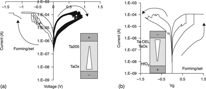
Similar inclination as the HfOx-based system for a preferred bi-polar operation, biasing and related engineered oxygen vacancy asymmetry is demonstrated for TaOx-based RRAM. Figure 9.24(a) shows dc behavior for a TaOx-based stack consisting of a deposited thin Ta-OEL followed by a deposited thick highly sub-stoichiometric TaOx, and then a thin stoichiometric Ta2O5 layer. The preferred bi-polar operation of this stack is as expected with Reset-anode against the good, or more stoichiometric, Ta2O5 side of the stack. Furthermore, a stack having near 1 nm stoichiometric HfO2 deposited and capped with thick sub-stoichiometric TaOx and then a thin Ta-OEL (Fig. 9.24(b)) demonstrates similar switching as the RRAM stack with a single thicker HfO2 with the top deposited OEL (Figs 9.19 to 9.21), where the preferred Reset-anode is opposite the vacancy-rich OEL/top electrode (and against the more stoichiometric side of the stack). The similar Reset for these different RRAM material stacks also supports the Reset mechanism of oxidizing the CF tip toward a thin (~ 1 nm) dielectric barrier,55 and since both films (Figs 9.20(a and b)) do have HfOx at the Reset-anode, they both form the similar approximate 1 nm HfO2 tunnel barrier with similar I-V characteristics.
9.4.3 Real-time monitoring of RRAM switching highlights operating mechanims
The relevant mechanisms for the bi-polar RRAM operation can be highlighted by capturing changes in the device conductivity in real time during applied Set or Reset type ac bias to the RRAM stack.6,7 For instance, in general, a dielectric barrier limiting the current in the HRS should break similarly irrespective of polarity of the applied bias; however, there is a clear difference in the HRS when pulse voltages of the same pulse width and height but opposite polarities are applied.62
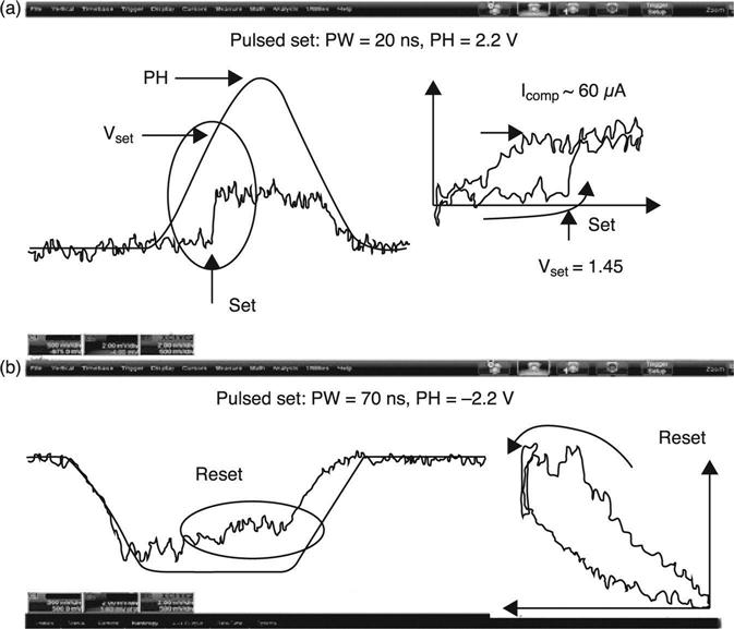
For preferred Set-type bias (Set-anode bias near the defect/vacancy-rich side) applied to the device in the HRS, a clear abrupt change to a lower resistance state occurs (Fig. 9.25(a)): the dielectric barrier abruptly breaks (when the electric field across the barrier approaches the critical hafnia breakdown field value [> 4 MV/cm subject to dielectric stoichiometry]), with the released negatively charged oxygen ions being pushed away from the barrier and toward the anode by the electric field. Due to lack of ‘available’ oxygen pushed toward the break in the dielectric barrier, and a higher oxygen vacancy concentration (from asymmetrical oxygen vacancy engineering of the fabricated TMO stack) near the anode for this Set-type bias, the reformation of the conductive filament occurs readily. For preferred Reset-type bias (Reset-anode bias opposite the defect/vacancy-rich side) applied to the device in the HRS, many continuous pulses are required before any resistance change occurs (Fig. 9.25(b)). In addition, when the resistance does change, the read current is noisy. According to the above-discussed model, higher barrier stability against the ‘preferred’ Reset-bias stress results from competition between the Hf-O bond breakage in the dielectric barrier, and the near immediate re-oxidation of the Hf atoms caused by a continued presence of the oxygen ions in their vicinity: the applied field pushes the ions against the electrode, thus preventing their fast out-diffusion from the filament region and providing ample available oxygen for filament tip oxidation.

Figure 9.26 shows oscilliscope captured switching data for a pulsed width (PW) of 20 ns for Set, and 70 ns for Reset, for fully integrated 1T1R HfOx-OEL RRAM in 100 nm × 100 nm cross-bar devices (similar RRAM stack as used in Figs 9.19 to 9.21).62 Switching for both Set and Reset between HRS and LRS in a similar ns time frame is clearly observed. In addition, for the preferred operational biasing, even at this ns time scale, the immediate and singular resistance change is observed for Set operation, and more noisy increase/decrease fluctuations in resistance are observed for Reset operation, due to the Reset bias additionally having an effective competition between oxidation of the CF tip to form a dielectric barrier, and breakdown of this developing dielectric barrier.
Optimizing RRAM switching requires an understanding of how asymmetrical oxygen vacancy profiles and filament geometry assist the nature and preference of the bipolar biasing operational schemes. The goal is creating a vacancy profile that is advantageous for dielectric barrier formation (from CF tip oxidation) during Reset, and dielectric barrier breakdown (filament re-formation) in Set operations, at conditions benefiting high speed/low power switching.
9.4.4 Performance and tunability
The reported results show that vacancy profile engineered HfOx-based RRAM can demonstrate robust low power operations, which appear to satisfy performance/endurance requirements for many applications of advanced memory systems. Key RRAM performance parameters, including LRS and HRS resistance, Set/Reset voltage and switching time, have been measured as a function of compliance current during Set (Icomp), applied voltage range and pulse speed (dV/dt) using real-time ac methodology, as well as dc characterization.6,7 For this study, fully integrated 50 nm × 50 nm cross-bar HfOx-based 1 T/1R RRAM devices with low parasitics were used. Unless noted differently, measurements were made on the same device, and trends were confirmed on multiple devices/wafers. An example of the dc I-V characteristic trends during HfOx-RRAM Set/Reset operations with increasing Set-Icomp levels is shown in color Plate XV.7
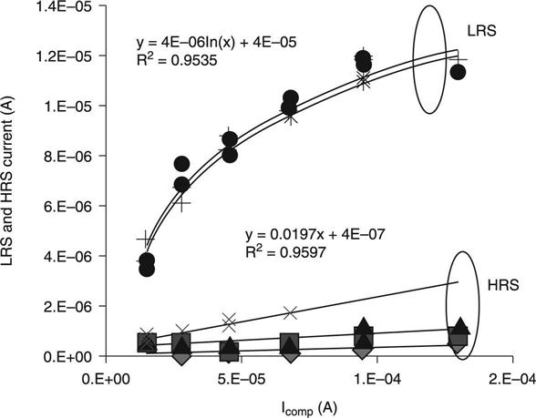
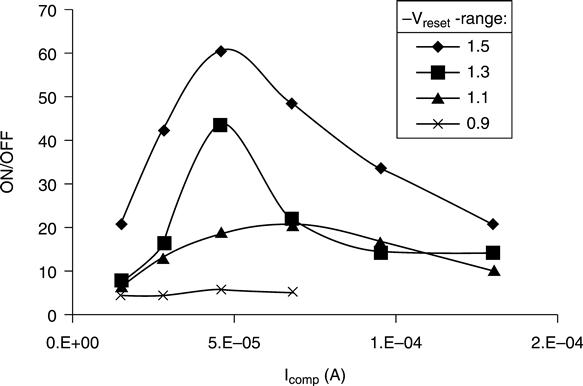
It has been demonstrated that capacitive parasitics can render the low resistance states after forming to have a strong dependence on the forming voltage VF.27 The properties of HfOx-based RRAM, when examined in devices using integrated 1T1R with low parasitics, demonstrate that the LRS is primarily controlled by the Icomp during forming operation (Fig. 9.27) for filament resistance vs forming-Icomp. Similarly, in Set operations, with the low parasitic integrated 1T1R, the operating LRS is primarily determined by Icomp during Set (see color Plate XVI for Set-LRS vs Set-Icomp for a wide range of Icomp).6,7 In addition, due to relatively low Vset values, any potential parasitic capacitance effects are small. The LRS current reveals a logarithmic dependency on Icomp in dc Set operation, while the HRS current exhibits only a weak linear increase with these Icomp limits (Fig. 9.27).6,7 These LRS and HRS resistance trends with Icomp result in the bell-shaped Ion/Ioff feature shown in Fig. 9.28.6 The smaller On/Off ratio with reduction of the Vreset-range is due to thinner oxidized portion of the filament in Reset, which leads to a lower HRS resistance. For increasing Vreset-range, a thicker and/or more robust dielectric barrier is formed having higher HRS resistance,57 which results subsequently in higher Vset required to break the ‘thicker’ formed dielectric barrier (Fig. 9.29).6

Thus, to paraphrase these dc trend observations; the magnitude of Icomp during Set is the major parameter controlling the LRS (via the filament cross-section), whereas HRS (determined by the dielectric barrier at a given filament crosssection) is mainly controlled by the Vreset-range. A more resistive HRS resulting from higher Vreset-range leads to a subsequently higher Vset.
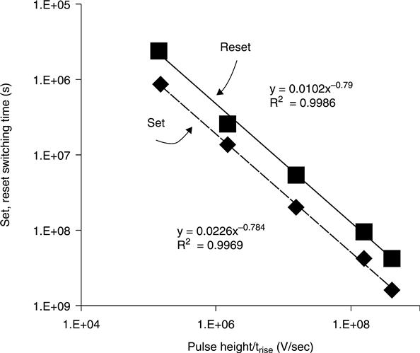
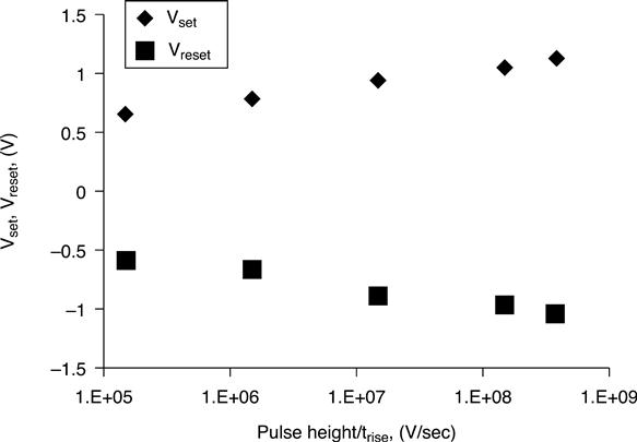
The ac operating kinetics for these devices have been examined using the real-time operation/monitoring methodology, which can measure the current through the RRAM during pulsed forming and Set/Reset switching to achieve accurate determination of switching voltage, and Set/Reset switching time.6,7 The HfOx-based RRAM devices can switch rapidly, down to the ps regime.10 It is observed in Fig. 9.30 that the faster the pulse (as defined by the pulse ramp rate: pulse voltage magnitude/pulse rise time), the faster the switching (between the LRS and HRS). However, the trade-off for increased pulse rise time (faster pulsing) is an increase in the minimum Vset and Vreset required to similarly change the device resistance state (Fig. 9.31).6
Although retention characteristics have not been discussed, reports of well-behaved retention (predicted beyond 10-year operation) above 200 °C for HfO2-based RRAM have been published.10 The promising retention behavior, is based on the structure of the conductive filament, and related structural changes, which for the case of HfOx-based RRAM involves the movement of atoms as opposed to the ‘incumbent’ charge-trap flash technologies that utilize the storage of electrons. Compared to the latter, the energy barrier of the atomic movement can be high, which impedes spontaneous structural re-arrangements, thus preserving the material’s resistive state.
In summary, operating performance, tunability and intrinsic dependencies have been established between switching voltage and HRS/LRS resistance, which in turn depends on the Icomp, and Vreset range. It is further established that HfOx-based RRAM devices integrated with a low parasitics selector (as in 1T1R) can achieve low power, high speed, and high endurance operations that appear to satisfy requirements for many memory systems.
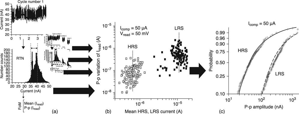
9.5 Read current instability (random telegraph noise)
The read current in RRAM is observed to exhibit stochastic digital-like changes of various amplitudes (Fig. 9.32).8,69–73 This instability, called random telegraph noise (RTN), effectively reduces a memory window limiting further scaling of operational currents. In this section, we focus on analyzing the RTN-induced read instability amplitude in a statistically significant number of cycles of individual HfOx-based RRAM cells (TiN/HfOx/Ti-OEL/TiN RRAM), which is also representative of the switching in idealized arrays of identically formed cells.

9.5.1 Statistics of read instability
The maximum variation of the read current, called Peak-to-peak (P-p) amplitude (Fig. 9.32),74 is associated with the event when all possible random changes occur simultaneously producing the maximum current fluctuation, which constitutes the worst case scenario from the standpoint of an erroneous read of the memory state. Therefore, the P-p amplitude can be used as a figure of merit (FoM) for a quantitative evaluation of the read instability in both high (HRS) and low (LRS) resistance states. The sometime observed irreversible step-like changes in the read current, which can be caused by generation/annihilation of an atomic defect contributing to the charge transport,74 are not considered here.
By establishing a functional dependency of the distribution of the collected RTN data over statistically significant number of cycles, it is possible to assess the maximum P-p amplitude, which may get potentially realized in the given device. The distribution of the P-p amplitudes (on a log-scale) is found to be fitted very well by the Gaussian probability density function (p.d.f.), yielding the most probable maximum noise amplitude and its dispersion value (Fig. 9.33). These two parameters define the entire P-p amplitude distribution in both LRS and HRS, allowing estimation of the probability of an RTN signal of any given amplitude to occur in this device. For successful reads of the resistive states, the memory window should be larger than the maximum noise amplitude. Therefore, the latter determines the minimum memory window necessary to keep the signal/noise ratio under a given limit.
This approach was employed to analyze the effect of RTN with scaling of the read current through scaling of the filament size.75 Both IHRS and ILRS (at the same read voltage) are usually smaller in devices formed under lower current compliance (Icomp) limits, which lead to smaller filaments,53 while the P-p amplitude is also found to reduce with the Icomp. The fact that the noise reduces proportionally to the memory window (color Plate XVII) is favorable for achieving lower operating currents by forming devices at lower Icomp.
9.5.2 RTN origin
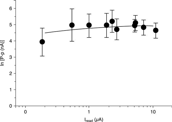
The RTN characteristics can be understood within the framework of the HRS/LRS description discussed in Section 9.3. In HRS, a current through the disrupted portion of the filament is shown to be supported by the trap-assisted-tunneling process (Fig. 9.18).25,53 Therefore, RTN of the read current in HRS is caused by the fluctuation of the number of traps contributing to TAT. As was discussed in Section 9.3, the TAT-active traps are the V+ oxygen vacancies in HfO2, which are created by the activation of the V(2 +) vacancies when they capture injected electrons.76 The process responsible for RTN is thus stochastic activation/deactivation of electron trapping/detrapping in some of the electron transporting V+ defects (Fig. 9.34). Each Reset/Set cycle results in the conductive filament being ruptured and restored, each time having a slightly different number and spatial distribution of V(2 +) defects that translate to different characteristic times of the V(2 +) → V+/V+ → V(2 +) processes and is subsequently reflected in variations of Iread and RTN signals.

The RTN model has been verified by comparing its prediction to the measured P-p dependency on the forming Icomp conditions. First, by using a single set of the earlier reported trap characteristics,25 the IHRS currents were calculated for various random spatial distributions of vacancies in the dielectric barrier in the devices formed under different Icomp conditions used to obtain the data in color Plate XVII. The fitting of the calculated IHRS, averaged over different randomly generated trap distributions, to the measured IHRS data (averaged over 200 switching cycles) yielded a number of traps (N) required to reproduce the HRS read current for each Icomp limit. Conductive filaments of larger cross-sections (i.e. formed at larger forming compliance currents) are found to contain a larger number of traps contributing to TAT transport, as expected (Fig. 9.34).
The extracted number of the traps contributing to IHRS for each Icomp was used to check the feasibility of the RTN being controlled by the fluctuation of this number due to the spontaneous activation/deactivation (V(2 +) → V+/V+ → (V2 +)) of some of these traps. The activation/deactivation rates for N randomly distributed traps were calculated using the above-discussed multi-phonon description. The Markov chain theory was then employed to calculate the probabilities, P(s), of finding a system of N vacancies in any of the 2N states, s = {1,2,…,2N}, when each vacancy is either active (V+) or inactive (V(2 +)) based on the above-mentioned activation rates. Using these probabilities, calculated separately for devices formed at each given Icomp, the dispersion of the theoretically simulated IHRS current fluctuations, with respect to its average value < IHRS>, can be evaluated:
[9.9]
Here σ is averaged over the various random trap distributions employed to simulate IHRS at each Icomp limit. This current fluctuation, σ, should correlate to the mean value of the P-p distribution measured in devices formed under a given Icomp condition. Indeed, each cycle potentially realizes one of the possible distributions of N vacancies, and for each of these distributions, the most likely current fluctuations (= P-p value in a given cycle) are determined by the vacancies (at configuration s) with the higher activation/deactivation probabilities (P(s)). In the example in Fig. 9.35, the 2σ range, which represents about 98% of the possible IHRS current fluctuations in any given Set/Reset cycle, resulted in an excellent agreement with the experimental (P-p) values obtained from 200 consecutive Set/Reset cycles. This agreement confirms that the HRS RTN can be associated with the traps in the oxide barrier in the filament.
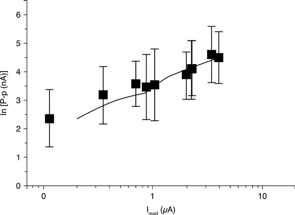
In contrast to the HRS case, the traps responsible for RTN in LRS may reside outside of the filament (Fig. 9.36) and, therefore, do not directly support the electron current through the RRAM cell. To describe the dependency of the noise amplitude on Iread, the Iread fluctuations were modeled by assuming that they are associated with a change in a partial Coulomb-blockade of the electron flux through the conductive filament caused by a change of a charge state of the nearby defect after it captured an electron. The CF section affected by the Coulomb blockade is located within a few Debye lengths from the charged trap. Theoretical values of RTN amplitudes for the CF of different sizes (which correspond to certain Iread values shown at the x-axis in Fig. 9.37) were calculated as P-p = Iread-c-Iread, where Iread and Iread-c are the simulated CF currents before and after the electron trapping at the adjacent defect. Iread is obtained by numerically solving Poisson and current continuity equations within the approximation of a uniform charge flow in the CF. Results in Fig. 9.37 show that the LRS P-p amplitude begins to scale with Iread only at its smaller values, when the trap effective blocking distance is becoming comparable with the entire filament cross-section. Note that a reduction of P-p(Iread) may also be associated with a change in the filament composition when it was formed at low Icomp (as manifested by a non-Ohmic conductivity, indicating a transition in the charge transport to the TAT regime).

The HRS and LRS trends of the P-p amplitude vs the read current magnitude reflect on the difference between the transport mechanisms in these states. The RTN can be attributed to the activation and deactivation of the electron traps in or near the filament and the effect of these processes on the electron transport through the RRAM cell.
9.6 Conclusion
Detailed operational and intrinsic switching characteristics for hafnia-based RRAM have been presented, including performance and tunability along with materials/vacancy engineering ramifications. The entire set of reported experimental data and material structure modeling and transport simulation results are consistent with the physical picture of the hafnia-based RRAM operations, as caused by oxidation/reduction processes in the conducting filament formed in the dielectric. The outcome of the filament formation process – an oxygen-deficient region (which constitutes a conductive filament) surrounded by the interstitial oxygen ions expelled from the filament region – establishes initial structural conditions for the subsequent Reset and Set operations. Kinetics of these redox processes can be considered by accounting for oxygen ions diffusion driven by the local electric fields and temperatures in the dielectric surrounding the filament. A microscopic description of these processes, the framework of which is presented here, directly links the device electrical and material characteristics, thus enabling improving device performance through optimization of the material compositional profile and operation conditions.
By nature of this approach, the resulting mechanism is material-specific, meaning that it explicitly includes dependencies on dielectric morphology (crystallinity and grain boundaries density), its stoichiometric profile (oxygen vacancy distribution), parameters of the electron-phonon coupling of the defects supporting electron transport in this material (e.g. ionization and relaxation energies of positively charged oxygen vacancies at GBs), processes of the oxygen-vacancy pair generation (metal-oxygen bond breakage), and diffusion of the released oxygen ions (hopping via substitutional oxygen sites). Ideally with any model there are no ‘fitting parameters’, however, it is important to realize the values of all parameters used in the simulations described are obtained outside the model, either from physical characterization data or material structure modeling, although there is always some uncertainty in even these parameter values.
At any given moment during the device operation, the processes of ion hopping and ion-vacancy pair generation/recombination at each location in the device are determined by the ion/vacancy distribution in the entire active device region, since it affects the local electric fields and temperatures. Due to essentially non-local characteristics of these processes and their probabilistic nature, an analytical compact description for the physical changes associated with the device switching is not feasible. Developing a simplified compact model, which would retain all essential properties of the comprehensive Monte Carlo description, presents a challenging but highly valuable goal. Alternative approaches allowing a compact description are phenomenological models, which are usually focused on specific features of the switching phenomenon (e.g. dependency of Reset time on the applied voltage), and utilize values of the employed parameters that are extracted by fitting the modeling results to the experimental data. These models can be helpful in explaining certain observations in a given material stack; however, they are generally less sensitive to the specifics of the material characteristics and therefore may not be as useful in driving fabrication process improvement as is the atomistic model described in this chapter.
Using the developed models and resulting understanding of the primarily driving forces for RRAM switching and their ramifications towards material properties, materials engineering of the HfOx-based RRAM was employed to optimize device performance. Based on the modeling results, the operating conditions leading to lower switching and device-to-device variability were identified. It is demonstrated that a sub-stoichiometric dielectric film with an asymmetrical vacancy profile is advantageous for effective dielectric barrier formation during Reset and dielectric barrier breakdown in Set operations, which are the processes controlling the switching in the bi-polar operated HfOx-based memory cells. The highly scalable and robust (> 300 billion cycle endurance) devices, which can operate at the ~ ns time scale at low power (~ pJ), fabricated using materials already common to the integrated circuits industry, exhibit a performance considered to meet a variety of NVM applications. Through continued refinement of developed models and materials engineering, it is expected that these RRAM devices will be successfully implemented for high volume manufacturing of commercial products.
9.7 Acknowledgements
The authors would like to thank the SEMATECH FEP memory team for their valuable discussions and contributions, and the CNSE Engineers and Fabrication line for efforts to help fabricate the RRAM devices.