Nanowire phase change memory (PCM) technologies: principles, fabrication and characterization techniques
M. Longo, National Research Council, Italy
Abstract:
This chapter reviews the various strategies for scaling down phase change materials to improve device performance. It reviews the advantages of phase change nanowires (PC-NWs), top-down and bottom-up fabrication processes and characterisation techniques; technological aspects are also considered. Special focus is placed on the self-assembly of NWs by the vapour-liquid-solid mechanisms, including metalorganic chemical vapour deposition. The compositional and structural analysis of NWs is reviewed.
Key words
nanowires; 1D structures; phase change memory; chalcogenide materials; nanoscaling; power consumption
6.1 Introduction
Interest in phase change memory (PCM) devices as future high performing, non-volatile and non-charge based memory devices is increasing. They offer high-speed operation, endurance and downscaling, even beyond lithographic limits (Bez 2009; Lacaita and Wouters 2008; Raoux et al. 2008; Terao et al. 2009; Welnic and Wuttig 2008). The first PCM devices were commercialized in 2010 by Micron (a 128 Mbit vehicle, http://news.micron.com/releasedetail. cfm?ReleaseID = 466859) and by Samsung (a 512 Mbit device), and currently some mobile phones are equipped with PCM devices.
The information in a PCM device is stored in the different structural phases of the active material, typically chalchogenide compounds such as Ge2Sb2Te5 (GST). Suitably different values for the electrical resistivity correspond to these phases (even by 3–4 orders of magnitude) and can be used to assign binary codes. Reversible structural changes are induced in the compound by proper energy transfer, in the form of ns current pulses that induce Joule heating. A critical aspect is related to the crystalline to amorphous transition (reset operation), for which the material has to be melted and then rapidly quenched. Melting temperatures as high as around 600 °C are required for this process in the case of GST, with the result that relatively high reset currents (fractions of mA), and therefore high power (fractions of mW), are required in PCM devices (Burr et al. 2010), in comparison with mature Flash memory technology. However, crystallization temperatures are lower (~ 160 °C for GST), so that the amorphous to crystalline transition requires less energy. Therefore, although PCM devices are promising in terms of their fabrication costs, important issues for future development of PCM devices are the increase of the storage capacity per cell and the reduction of power consumption and costs.
6.2 Strategies for improving the PCM performance
Storage capacity and power reduction of PCMs can be basically achieved by acting on the phase change material and/or on the programming volume size, meaning scaling down the memory cells.
6.2.1 Modifying phase change materials
Firstly, alloys are required that can compromise between the high crystallization rate and the stability of the amorphous phase. Typical PCMs have a 10-year data retention; they keep the information correctly stored for that entire time period, at temperatures of at least 105 °C (Redaelli et al. 2005). The ability to retain data and maintain the memory behaviour at the nanoscale is determined by the stability of the amorphous phase change material against spontaneous recrystallization and its dependence on both composition and interfaces. For example, variations of the composition within the largely employed Ge-Sb-Te system are known to have an impact on the speed/retention trade-off. The crystallization temperature can be increased by increasing the content of GeTe within the (GeTe)x(Sb2Te3)y sub-system, thus improving the stability of the amorphous phase, although this entails some drawbacks for the crystallization speed. It has been reported that there are great improvements to the data retention when nitrogen doping around 10% is employed in GeTe, yielding data retention of 10 years at 241 °C (Peng et al. 2011). However, such a trade-off has not been clearly assessed yet. Currently, GST is used in PCMs, due to its fast crystallization dynamics and its high stability at operating temperatures. Memories based on using GST have shown 10 years retention for temperatures up to 110 °C (Pirovano et al. 2003), which is sufficient for several applications, including mobile phone cards.
For automotive applications, the 10-year retention is required at a temperature of 125 °C (Morikawa et al. 2007). A higher retention temperature corresponds to a higher stability of the amorphous phase, and therefore to a higher crystallization temperature. For this application, GST has a high melting temperature (TM ~ 620 °C), but too low a crystallization temperature (TX ~ 160 °C), and insufficient multi-bit storage capability. ‘In-based’ chalcogenide materials, namely those belonging to the In-Ge-Te and In-Sb-Te systems, display higher thermal stability: In-Ge-Te (IGT) has a very high crystallization temperature (TC ~ 276 °C) and a 10-year retention at 170 °C (Morikawa et al. 2007). In3Sb1Te2 (IST) has an even higher crystallization temperature (TC ~ 280 °C) (Maeda et al. 1988). Recently, In-based chalcogenide materials are increasingly being considered for PCM application and some reports of In-based PCMs can be found in the literature (Daly-Flynn and Strand 2003; Kim et al. 2009, 2011; Morikawa et al. 2007).
6.2.2 Reducing volume size
A very effective method of power reduction reduces the size of the chalcogenide-based memory cells to the nanoscale (~ 100 nm). Lowering the active material volumes that are to be programmed allows for reduced power consumption and at the same time increases the cell density. Of course, this needs to be done by assuring the conservation of the basic material characteristics, even for very small dimensions. The scalability of PCM cells has been demonstrated down to 1.8 nm for GeTe nanoparticles, and Caldwell et al. (2012) have obtained writing currents as low as 1.4 μA, 1000 times lower than in ordinary PCM devices, by using carbon nanotube electrodes, with good prospects for high volume manufacturability and reliability.
Actually, different scaling rules are related to the PCM cells (Lacaita and Wouters 2008), so that the scaling of the active material/bottom electrode contact area (Ha et al. 2003), cell confinement in trenches/pores (Pirovano et al. 2008) and 3D cross-bar architectures (Sasago et al. 2009) are being explored for their potential in power consumption limitation. The best programming energy reduction and fast switching have been obtained in Interfacial Phase Change memory (IPCM) devices by the use of ultra thin GeTe/Sb2Te3 superlattices (Simpson et al. 2011). In the Interfacial PCM, the switching energy is reduced, because the movement of the atoms is limited to a single dimension. The phase change would not occur by conventional melting, and therefore would require much less energy. The electrical energy required to set the interfacial phase-change memory cell was reported to be as low as 11 pJ, whereas for conventional GST cells the same authors reported 90 pJ (Simpson et al. 2011).
Most of the GST thin films used in current PCM applications are obtained by physical deposition, such as sputtering, which is limited by its low deposition conformality, i.e. it is unsuited to provide uniform filling of structured substrates, especially for vertical, high aspect ratio ones. In order to fabricate ultrascaled memory cells, more conformal techniques are needed to uniformly deposit GST inside structured substrates with trenches tens of nanometers wide. Among the growth methods that can provide highly conformal deposition, atomic layer deposition (ALD) and metal organic chemical vapour deposition (MOCVD) are being explored. Scaled PCM devices have already been realized by MOCVD and mixed ALD/CVD processes (Choi et al 2009; Fallica et al 2013; Lee et al. 2007).
An alternative method for reducing programming volumes and contact size areas is to employ phase change nanomaterials, synthesized either by top-down or bottom-up approaches. Some different approaches to achieve this are:
• the use of metal sidewall pattern technology (Lv et al. 2006);
• Sb-doped Te-rich nanotubes synthesized by the vapour transport method (Jung et al. 2011);
• sputtered GST in carbon nanotubes (Xiong et al. 2009);
• GST nano-pillars fabricated by nano-imprint lithography (Bae et al. 2009);
• GST nano-rings created by focused laser beam followed by differential chemical etching (Chu et al. 2011);
• phase change nanodot arrays by the lift-off technique on a self-assembled di-block copolymer template (Zhang et al. 2008);
• nano PCM cell element obtained by using a Focused Ion Beam (Liu et al. 2005);
• colloidal GeTe nanocrystals (Caldwell et al. 2010);
• metal chalcogenide arrays created by using Block Copolymer-Derived Nanoreactors (Milliron et al. 2007).
6.3 The use of nanowires
The use of 1D phase change structures, such as nanowires (NWs), makes it possible to fully exploit the scaling properties of the PCM device. The phase change NW growth and its diameter, composition and crystallinity can be controlled. In this way, a NW can form a nano PCM cell itself. If dense arrays of NWs are obtainable, a further novel highly performing device could be formed: a NW phase change memory cell, with a relatively low manufacturing cost. The energy required to induce the phase transition is lowered, not only because of the good structural properties of these nanostructures (which can be defect-free when the NWs are self-assembled) and the high geometrical scaling, but also due to other aspects related to size effects (Chapter 7).
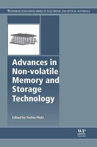
The idea of a NW-PCM device is very simple, based on the transformation of the active chalcogenide layer in a planar cell into a 1D cell. A small volume in the region close to the bottom electrode heater is crystallized and re-amorphized during the switching cycles of a planar PCM cell. The 1D cell is formed by a nanowire, whose metallic contacts at both tips form the top and bottom electrodes, respectively. A nanocell is therefore obtained in which the NW is a self-heating resistor. A portion of it undergoes a phase transition from amorphous to crystalline, as the current flows through it. A proper dielectric material is needed to passivate the NW, not only to insulate it, but also to protect it from evaporating during the phase transitions. Figure 6.1 displays the schemes of a planar PCM cell and a NW-based PCM cell.
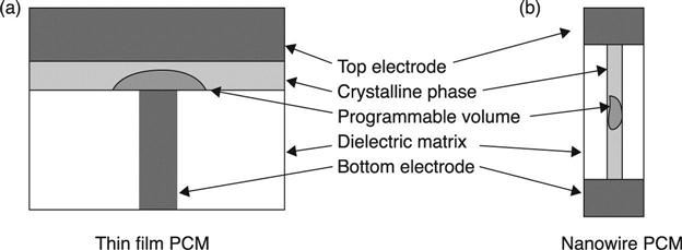
The alloys used for phase change nanowires are essentially the same as those used for planar PCM cells. They belong to the IV, V and VI groups of the periodic table and aim at high speed transitions, a large resistance window between the amorphous and crystalline phases, thermal stability of the amorphous phase (for data retention) and a high number of transitions before material degradation (cyclability). GeTe, Sb2Te3 and the alloys of the pseudobinary GeTe-Sb2Te3 tie line (in particular the stable phases Ge2Sb2Te5, Ge1Sb2Te4 and Ge1Sb4Te7), are the main alloys that have been investigated, along with In2Se3, Ge-Sb, Bi2Te3, InSb and In3Sb1Te2. The next section will illustrate examples of the most commonly used materials for phase change nanowires and their corresponding synthesis techniques. In Fig. 6.2, the different alloys used for phase change optical and electronic memories are shown. In the case of optical data storage, different material reflectivity of the amorphous and crystalline states is looked at, instead of electrical resistivity.
6.4 Fabrication of phase change nanowires (PC-NWs): top-down approaches
In the case of NWs based on III-V and nitride compounds, it is possible to obtain such structures either via the ‘top-down’, or the ‘bottom-up’ approaches. The top-down approach involves patterning processes. It mainly employs lithographic techniques, based on ultraviolet (UV), X-ray and electron beams, or reactive ion etching (RIE), so that the NWs are obtained by properly removing material until the desired structures are exposed. This is the most compatible method with the current CMOS technology.
The bottom-up approach is characterized by the use of the basic constituent blocks (often the elements themselves), which are built up to form complex NW structures, using chemical reactions and/or self-assembly mechanisms on nanostructured or chemically active surfaces. The NW size, morphology and growth can thus be controlled in a single-step process. Moreover, structures such as core-shell NWs can be synthesized, which are not possible when employing top-down technologies.
Both the top-down and bottom-up approaches present positive and negative aspects. In terms of the top-down approach, the resolution of the chip-compatible lithographic tools is limited and the fabricated nanostructures may present some structural damages or defects. Equally, the defect-free NWs obtained by the bottom-up approach cannot be located at desired positions or interfaced in a device. Future applications will need to consider using a combination of top-down and bottom-up techniques. For example, an ordered array of phase change NWs could be obtained by allowing their self-assembly through selective area deposition on favourable surfaces areas, by using nano-patterning.
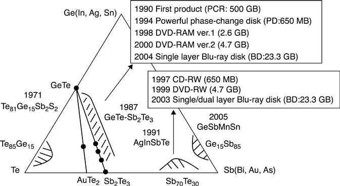
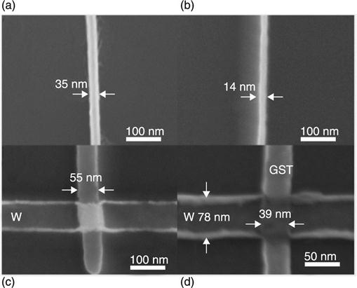
The use of PCM cells based on a single Sb-Te nanostrip, comparable to a NW, was first reported in 2005. These have been obtained by top-down fabrication, in particular by electron beam lithography (EBL) and RIE (Fig. 6.3). In this case, the reset current resulted as a function of the strip cross-section, but it was clearly advantageous that no heater integration was required. Analogously, the bridge cell concept was reported, in which a Ge15Sb85 nanowire was deposited on top of TiN electrodes by EBL coupled to Ion milling (Fig. 6.4), yielding a cross-sectional area of 60 nm2. In this case, a minimum 90 μA reset current was obtained. Ma et al. (2011) reported a so-called ‘self-aligned process’ to obtain phase change NWs (Fig. 6.5). These are self-confined in properly processed electrode nano-gaps which, after EBL, lift-off and inductively coupled plasma (ICP), form lateral PCM devices (Chen et al. 2006). The experimental set-up and the tested device are illustrated in Fig. 6.5.

6.5 Fabrication of phase change nanowires (PC-NWs): bottom-up approaches
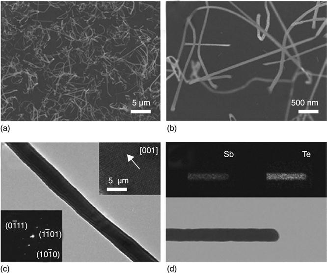
The bottom-up fabrication of phase change nanowires is generally based on a deposition process, coupled to self-assembly mechanisms. Bottom-up NWs are typically single crystalline, defect-free structures and thus ideal for studying size-dependent properties of the constituent materials. Physical deposition processes have been used, such as in the case of the Sb2Te3 NWs shown in Fig. 6.6. A 200 nm Al-Ge-Sb-Te thin layer (AGST, Al = 6.5–22.6 at.%) was deposited at RT by DC magnetron sputtering on a glass and on a Si(100) wafer by co-sputtering. SbTe NWs, 100 nm in width, were extruded spontaneously on the surface of thin AGST films for thermal annealing at around 300 °C and above 12.4 at.% Al content. The hypothesis was that the ‘thermal stress-induced growth’, namely the thermal mismatch between the substrate and the AGST layer inducing mass flow along grain boundaries upon thermal annealing which forms the NWs, is the dominating mechanism. Notably, this approach does not require the use of metal catalysts; on the other hand, many NWs appeared as kinked or curved.
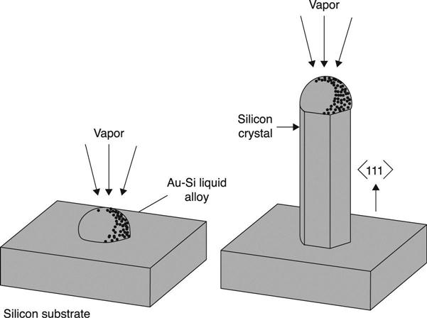
The most diffused technique for defect-free NW self-assembly makes use of chemical vapour deposition (CVD), coupled with vapour-solid (VS) and/or vapour-liquid-solid (VLS) mechanisms (Wagner and Ellis 1964). For the VLS mechanism, a metal catalyst is required to form a eutectic alloy at the substrate surface with the reactant vapours. The eutectic temperature is lower than the each element’s melting temperature, so that the alloy melts into a liquid droplet. Under supersaturation conditions, the droplet forms a site for the NW, which starts growing epitaxially at the droplet base, with atoms collecting at and then leaving the feeding droplet at the NW tip. The NW diameter is generally related to the catalyst size (Mohammad 2009; Shwartz and Tersoff 2009). This mechanism is shown schematically in Fig. 6.7.
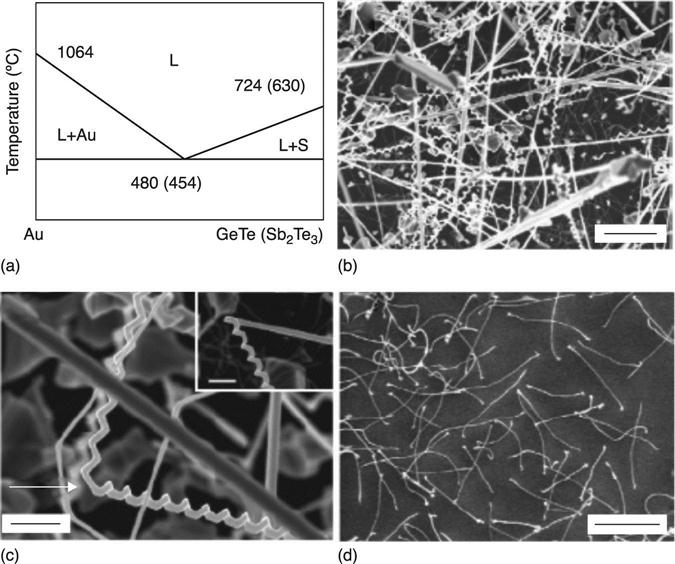
The phase diagram for Au (the most used catalyst) and GeTe-Sb2Te3 in Fig. 6.8(a) from Meister et al. (2006) shows that it is possible to reach the eutectic point at temperatures as low as 454 °C in the VLS deposition of Sb-Te (ST) NWs. This work showed how it is possible to grow Sb2Te3 and GeTe (GT) NWs using a VLS mechanism with different morphologies: from straight to helical to curly, even co-existing (Fig. 6.8 (c–d)).
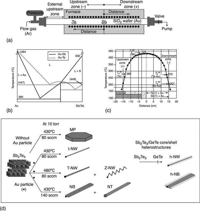
This mechanism is actually widely employed for phase change NW self assembly. This is shown in Fig. 6.9(a) (Lee et al. 2008), which depicts the typical scheme of a horizontal furnace that uses chemical vapour transport methods for the synthesis of NWs. By tuning the temperature profile in the furnace and the position of the sources (in this case Te and Sb), it is possible to ensure that they thermally evaporate at higher temperatures and then allow the Sb-Te NW self-assembly by VLS at a lower temperature (Fig. 6.9(b)). Different morphologies for phase change Sb2Te3 NWs could be chosen by changing the furnace temperature profile (Fig. 6.9(c)), the location of the reactants and the carrier gas flow, from straight to zigzag NWs, nanobelts and nanotubes (Fig. 6.9(d)).
 , melting temperature at 10 Torr;
  , eutectic temperature with Au at 10 Torr; and (d) morphologies of Sb2Te3 nanostructures controlled by the growth temperature and the Ar flow rate: MP, microplate; t-NW, thin NW; T-NW, thick NW; Z-NW, zigzag NW; NB, nanobelt; NT, nanotube; h-NW, core/shell NW heterostructure; h-NB, core/shell NB heterostructure. Reprinted with permission from Lee et al. (2008), copyright (2008), American Chemical Society.
In general, the growth conditions deeply influence the NW length and diameter, especially the growth temperature time and reactant concentration, as in the case of GeTe NWs. Complete control of the resulting NW is not always straightforward as it depends on the deposition method, conditions and the complex reactions that may take place (S.W. Jung et al. 2009). Once the reactant concentration is fixed, the growth temperature in the vapour transport methods can influence the composition of the NWs, as demonstrated by Philipose et al. (2010) for InSb NWs and by Longo et al. (2012) for Ge1Sb2Te 4 NWs.
Many studies have reported the synthesis of phase change NWs by vapour transport methods in horizontal tube furnaces. These include single crystal GST (Jung et al. 2006, 2011; Lee et al. 2007, 2008), Ge-Sb (Jung et al. 2009; Sun et al. 2008), Sb2Te3 (Meister et al. 2006), GeTe (Jennings et al. 2009), In2Se3 NWs (Baek et al. 2013; Yu et al. 2007), Sb2Te3/GeTe (Lee et al. 2008) and InSb NWs (Philipose et al. 2010). Although controlling the composition of the NW was not straightforward in vapour transport techniques, it was finally achieved in GST NWs (Jung et al. 2013), producing peculiar superlattice structures in Ge8Sb2Te11, Ge3Sb2Te6, Ge3Sb8Te6 and Ge2Sb7Te4. The VLS method was also adopted to synthesize doped NWs, analogously to the case of phase change layers. Zhang et al. (2013) have investigated Bi-doped GeTe NWs, with a Bi content of around 3 at.%, in which the crystallization time is strongly reduced by a factor of 20 with respect to undoped GeTe NWs.
The self-assembly approach is fundamental for the realization of core-shell NW structures. These were demonstrated by Lee et al. (2008), who first grew Sb2Te3 core NWs by using VLS and vapour transport and then uniformly coated in situ, the core NW using a GeTe shell, through a vapour-solid growth. The results are shown in Plate I (see colour section between pages 268 and 269).
Such structures might not seem to have special applications, but this is not the case. They made it possible to design novel multilevel PCM devices, in which further information can be stored beyond the set (0) and set (1) binary codes. The possibility of obtaining multilevel PCM was already explored in thin films by Rozenberg et al. (2004). The drawbacks related to poor control of the crystalline and amorphous states, a narrow programming window and unsatisfactory reproducibility. A multi-layer phase change material stack, formed by Nitrogen-doped GST and GST layers sandwiching a Ta2O5 barrier layer, was reported by Gyanathan and Yeo (2011) to exhibit a resistance window of one order of magnitude.
The GST/GeTe CS-NWs by Jung et al. (2008) (colour Plate II) demonstrated that the way to remove such limitations is to couple different phase change materials, which have different electrical and thermal properties. The deposition was performed by VLS growth of the GST core NW, followed by the conformal deposition of the GeTe shell by vapour-solid growth. This kind of structure can yield multilevel programming, due to the introduction of intermediate resistive states.
The vapor transport growth is limited by factors including low flexibility, difficult compositional tuning and industrial transfer. Other possibilities for improving this are offered by advanced chemical deposition techniques, such as the Metal Organic Chemical Vapor Deposition (MOCVD) technique. This provides good control of the material composition, high purity, industrial scalability on 12″ substrates and relatively high deposition rates. In MOCVD, the vapour phase transport is achieved using metalorganic compounds (precursors) and/or hydrides of the atomic species to be deposited. The deposition occurs through the pyrolysis (endothermic dissociation) of the precursors, which makes the atomic species available when under thermodynamic super-saturation conditions. The technique is highly flexible in terms of the choice of reactants and the deposition parameters and allows large area deposition, thus potentially enabling large-scale NW assembly.
Notably, only one paper has been published on the self-assembly of GeTe, Ge-doped Sb-Te and Ge1Sb2Te4 NWs using the MOCVD coupled with the VLS technique (Longo et al. 2011, 2012, 2013). The only current report on the MOCVD synthesis of IST NWs was based on overpressure deposition (Ahn et al. 2010). Single crystal GeTe NWs, with a length up to 4 μm, were obtained using the MOCVD technique (Longo et al. 2011). The effect of the catalyst size was studied and longer NWs obtained by using 10 nm islands, whereas 50 nm islands induced NW self-assembly with a higher diameter and more dispersed length. The NW aspect ratio was in the range of 10 to 16.
The same synthesis mechanism was found in Ge1Sb2Te4 NWs by MOCVD and VLS (Longo et al. 2012) (Fig. 6.10). However, in this case, the length distribution was centred at around 400 nm. Since they were deposited on SiO2, NWs showed different orientations with respect to the substrate. Furthermore, background crystals were formed where larger Au islands did not induce NW formation. Notably, this is the only report of Ge1Sb2Te4 NWs, which is independent of the deposition technique. Both GeTe and Ge1Sb2Te4 NWs could be grown at 400 °C, 50 °C below the lowest eutectic point of the phase diagram (Meister et al. 2006), indicating the effect of their size, namely that a sub-eutectic growth was possible.

Sb2Se3/Sb2S3 NWs were synthetized by pulsed VLS and CVD techniques by Yang et al. (2009). The molecular precursors were alternatively delivered to the Au nanocatalyst area in the form of pulses, to prevent pre-reactions and ensure better deposition control, in an analogous method to atomic layer deposition (ALD). No catalyst was used for the MOCVD synthesis of phase change In-Sb-Te NWs on the planar TiAlN/SiO2/Si substrates displayed in Fig. 6.11 (Ahn et al. 2010), so that even lower temperatures of 250 °C could be used. Here the driving mechanism was the protrusion under high supersaturation of InTe, caused by relatively high concentration of the reactants in the growth chamber, to which Sb was incorporated, forming IST NWs.
Lee et al. (2009) have reported on the liquid phase synthesis of orthorhombic GeTe NWs. Their assembly was induced by the presence of dispersed Bismuth seeds, demonstrating the potential for this method in terms of low production costs, low deposition temperature (below 300 °C) and high throughput. The NWs are shown in Fig. 6.12. Due to the absence of the Bi seeds at the NW tips, Ostwald ripening was proposed as the growth mechanism, rather than Solution-Liquid-Solid (SLS). The NW diameter ranged from 50 to 100 nm and their length was around 2 μm. Finally, Sb2Se3 NWs were deposited by microwave activated solvothermal reaction and reported by Metha et al. (2010).
6.6 Fabrication of phase change nanowires (PC-NWs): other techniques
6.6.1 Self-aligned nanotube-nanowire PCMs
Xiong et al. (2013) introduced a nanofabrication method called the self-aligned nanotube-nanowire PCM, using the aid of carbon nanotube (CNT) electrodes. This method does not require lithography to self-align the NWs and the CNTs. The nanogap in the CNTs is created by inducing electrical breakdown. The 10 nm of GST are sputtered in the PMMA nanotrench (previously induced by Joule heating). When the remaining PMMA has been removed, a tiny GST NW results, perfectly aligned with the CNT, which can be used as electrodes (Fig. 6.13)
A process that did not require lithography was also developed by Fu et al. (2013). They prepared GST NWs using an SiN x spacer as an etch mask, which formed a NW that was fully confined in a metal nano-gap. Such a device showed very low currents (16 μA) and set voltage (80 mV).
6.6.2 Template-based deposition
Further growth methods have been employed to self-assembly phase change NWs, in particular the template-based deposition (electrochemical deposition). This is a relatively simple method to fabricate low-dimensional structures. It uses an ionic solution containing the elements to be deposited on the surface of a conductive template by electrolysis. Anodized aluminium oxide (AAO) membranes containing nanopores are used to form the NWs. The NWs can be electrodeposited within the nanopores. By this method, arrays of Bi2Te3 NWs were deposited with diameters of around 25, 30 and 75 nm (Sander et al. 2003) (Fig. 6.14). Bi2Te3 NWs were also deposited into 70 nm pores of AAO membranes at a 10 mV voltage, using an electrolyte of HNO3, Bi2O3 and TeO2 (Han et al. 2011). To analyse single NWs, the AAO membrane could be dissolved in NaOH. In order to obtain a PCM cell device formed by NW arrays in the membrane, Au/Ti and Pt electrodes were deposited at the base and top of the NWs for electrical analysis. Notably, Bi-Te NWs with different compositions from Bi2Te3 did not exhibit the phase change behaviour.

Sb-Te NWs with variable compositions and aspect ratios were also electrodeposited into AAO membranes and amorphous Sb37Te63 NWs with an average diameter of 80 nm and length of 1.2 μm were grown by electro-deposition on homemade AAO templates with a good vertical alignment (Ihalawela et al. 2012).
6.7 Characterization of PC-NWs
The typical front-end characterization to check the NW formation is performed by SEM. This can also give an immediate indication of the possible VLS or VS mechanisms. The structure of the NWs is basically determined by their fabrication process. In the case of the top-down approach, NWs can be formed by either amorphous or crystalline material, depending on the starting layer. The attention is focused on the NW morphological properties, rather than the structure. The majority of phase change NWs are actually synthesized by bottom-up processes, often leading to crystalline NWs. In this case the NW composition and structure is carefully analysed, since the synthesis method can lead to significantly different structural and compositional properties, and therefore to different phase change behaviour. Moreover, the crystalline structures of the NWs may be different from those of the equivalent layers or bulk-like materials, because of their size.
A critical parameter is the synthesis temperature, which influences the crystalline phase of the NW when it is higher than the crystallization temperature of the involved material. It is useful to consider the case of GST, which is characterised by two transition temperatures:
1. the amorphous → face centred cubic metastable phase (fcc) transition around 150–170 °C; and
2. the fcc → stable hexagonal close packed (hcp) transition, around 260–300 °C, depending on the rate of temperature elevation (Kato et al. (2005).
Normally, the first transition is the one exploited in PCM devices. In the case of the largely diffused VLS mechanism, the NW synthesis temperature is higher than 300 °C, meaning that the GST NWs are expected to exhibit hexagonal crystal phases. Analogous issues can be examined once it is considered that GeTe has a crystallization temperature of 145 °C (Yamada et al. 1991) and Sb2Te3 has 77 °C (Damodara Das et al. 1987).
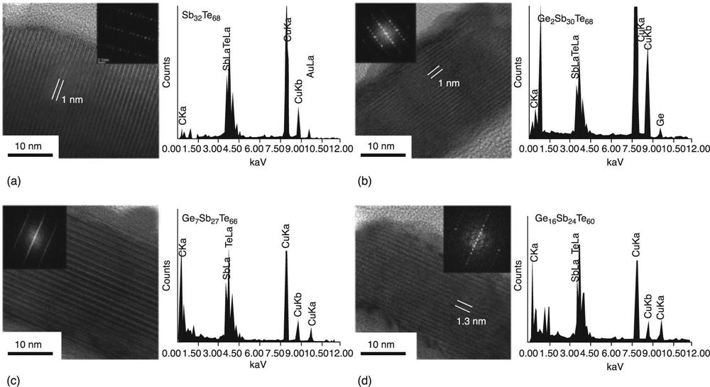
The study of the structural and compositional analysis of phase change nanowires is mainly based on high resolution transmission electron microscopy (HR-TEM), energy dispersive spectroscopy (EDS) and selected area electron diffraction (SAED) measurements that allow a local area analysis on single nanowires. Other techniques can be of use, such as X-ray fluorescence (XRF) and X-ray diffraction (XRD). However, XRD and XRF can only collect information over relatively large areas, which can be a limitation when non-uniformity in the NW structure or when other synthesis products are present, such as undesired background crystals. This is the case for GeTe NWs grown by MOCVD on SiO2 substrates (Longo et al. 2011). Although the VLS mechanism is clear from the presence of the Au tip, different NW orientations and background crystals can be observed by SEM when using Au nano-islands within average sizes of 10 nm (1L) and 20 nm (2L) as metal catalysts (Plate III in colour section between pages 268 and 269).
Total reflection XRF (TXRF) gave an overall composition of Ge0.46Te0.54 for the grown material, including the presence of the Au XRF peak. However, the XRD analysis indicated a compatibility of the recorded NW spectra with both rhombohedral and cubic GeTe structures. More reliable information came from the local area analysis, performed by TEM (see Fig. 6.15, related to a 50 nm wide NW), which showed a dark Au seed containing around 10% of GeTe. Notably, the VLS mechanism occurred in a sub-eutectic condition at 400 °C. Moreover, size effects induced the NW metastable cubic phase then normally expected at 446 °C (Mohammad et al. 2009). The GeTe NWs appeared to be single-crystal and defect-free and to grow along the [110] direction; the EDX analysis confirmed the stoichiometric composition. Another case in which cubic GeTe NWs orientated along the [110] direction were obtained, is reported by X. Sun et al. (2007). In other cases, rhombohedral GeTe NWs were observed to grow along the [220] direction (Lee et al. 2006), along the [–111] direction (Meister et al. 2008), along the [202] direction (Jennings et al. 2009) and along the [220], [003] and [202] directions (Yu et al. 2006). It is worth noting that in one case Bi-seed assisted GeTe NWs, synthetized by liquid phase growth, obtained orthorhombic NWs at very low temperatures (< 300 °C).

A peculiar oxidation effect was observed in GeTe NWs grown by VLS. Sun et al. (2007) found a 1 ~ 3 nm amorphous GeO2.TeO2 outer layer, after exposure to oxygen. This effect of oxidation was also observed by CNR-IMEM, Parma, Italy, in MOCVD-grown GeTe NWs. It was related to ageing, as the oxide layer thickness increases with the time exposure to air (Fig. 6.16). The Moiré fringes in Fig. 6.16 are the result of overlapping of the inner GeTe crystalline region of the NWs and of nanocrystals embedded in the amorphous layer. The nanocrystals, visible along the NW axis in the figure, were accurately identified to be composed of Te and the amorphous layer is mainly formed of GeO2. On the basis of these results, it can be concluded that oxidation tends to occur on Ge, with the Te excess aggregating in crystal clusters.

The Fourier transform (FT) of the HR image in the inset in Plate IV(a) (in the colour section between pages 268 and 269) displays the spatial frequencies caused either by the inner crystalline region or the Te particles. In colour Plate IV(b), the distribution of the spatial frequencies is mapped in a false colour image. This was obtained by performing the inverse FT (FT− 1) process for each frequency at a time and then by summing up all the obtained images. The intensities produced by the inner crystalline region and the outer Te clusters were very well separated. The ageing process is sketched out in colour Plate IV(c), where the dashed lines represent the initial wire walls.
Most of the work on the structural analysis of single crystalline Ge2Sb2Te5 NWs has been done by the group of R. Agarwal at Penn University of Pennsylvania, USA. They have worked on demonstrating the hexagonal hcp structure and the [001] growth direction (Lee et al. 2007). In another report, two dominant growth directions were identified, namely the [110] and [001] of the hcp structure (Lee et al. 2008). The only reported work related to the (MOCVD) synthesis and structural characterization of the stable phase for single crystal Ge1Sb2Te4 NWs was by Longo et al. (2012). The homogeneity of the alloy was evidenced by the uniform EDX mapping and profiles. The rhombohedral phase and growth directions were found to correspond to the [1–1 0 14] and [1 0–1 0] directions of the hexagonal structure, corresponding to the [1 0 0] and [1 1 2] growth directions of the rock-salt cubic structure (Fig. 6.17).

The atomic arrangement of the Ge-Sb-Te compounds is a matter for debate. Many different configurations have been proposed. Rotunno et al. (2013) have made progress with regard to the atomic arrangement of the rhombohedral structures in the stable phases of Ge2Sb2Te5 and Ge2Sb2Te5 NWs. They have identified the stacking sequence in their crystal structure through the comparison of experimental High Angle Annular Dark Field Scanning Transmission Electron Microscopy (HAADF-STEM) results and STEM simulations. Different sets of theoretical models, proposing possible stacking sequences, were chosen for comparison. Figure 6.18 shows the three models for the Ge2Sb2Te5 structure proposed by Kooi and De Hosson (2002), Matsunaga et al. (2004) and Petrov et al. (1968). Matsunaga et al. (2004) introduce the possibility of disorder in the Ge/Sb site occupation, since Ge and Sb are allowed to share the same lattice site in precise rates. ‘ν’ is referred to as the ordered vacancy layer. However, its possibility had been ruled out by theoretical works.
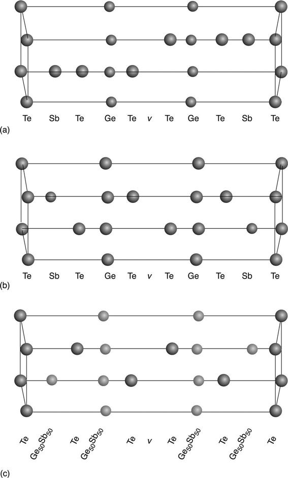
Figure 6.19 displays the experimental HAADF-STEM image from a Ge2Sb2Te5 NW and the simulations obtained from the models of Fig. 6.18. The darkest lines, separated by approximately 1.7 nm, are the vacancy layers. On the right, the corresponding line profile intensities are shown.
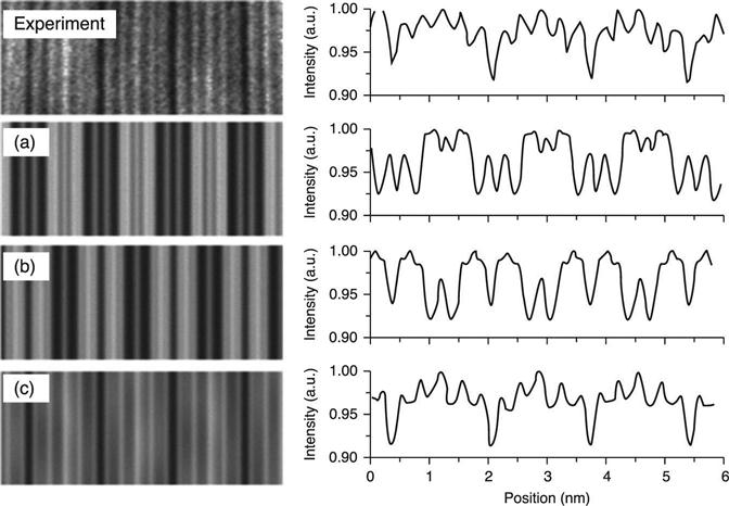
The highest cross-correlation coefficient, 0.866 (where 1 signifies coincidence), was obtained by the Matsunaga model, confirming that the structure in which Ge and Sb randomly share the same lattice sites does occur. Analogous conclusions were drawn in the case of the rhombohedral Ge1Sb2Te4 NW structure. This was found to crystallize with mixed occupation in the Ge/Sb planes, according to a similar model, also from Matsunaga, despite the adverse theoretical predictions (Matsunaga and Yamada 2004).
Jung et al. (2013) grew alternative Ge-Sb-Te NWs by chemical vapour transport. They controlled the composition of GeTe and increased the Sb content so that the value for x (calculated by: x = [Sb]/([Ge] + [Sb])) was varied between 0 and 0.8, in turn by varying the deposition temperature and the elemental sources ratio. Figure 6.20 shows the main results for the nanostructures. The interesting outcome was that the increase of the Sb content, substituting Ge, lowered the transition temperature from the rhombohedral to the cubic phase and introduced a phase evolution yielding polymorphism. In particular, the latter resulted in rhombohedral/cubic phase co-existence, zigzag NWs and superlattice structures, whose properties are summarized in Table 6.1. Pure rhombohedral structures were again obtained when the Sb content was above 0.7, supporting the expectation that the Sb content increase lowers the transition temperature from the cubic to the rhombohedral phase.
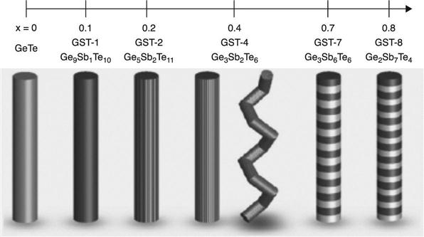
Table 6.1
Properties of rhombohedral/cubic phase co-existence, zig-zag NWs and superlattice structures
| No. | Diametera (nm) | xb | Composition | Crystal structurec | Growth direction | Periodd (nm) | No. of layerse | ρf (mΩ · cm) |
| GeTe | 100 | 0 | GeTe | R | [0111]R | 8.5 | ||
| GST-1 | 100 | 0.1 | Ge9Sb1Te10 | R and C | [110]C | 3.5s | ||
| GST-2 | 150 | 0.2 | Ge8Sb2Te11 | C | [110]C | 3.8 | 21(1) | 4.0 |
| GST-4 | 200 | 0.4 | Ge3Sb2Te6 | C and R | [110]C | 2.2 | 11(1) | 9.0 |
| GST-7 | 400 | 0.7 | Ge3Sb8Te6 | R | [0001]R | 3.4 | 17(0) | 2.0 |
| GST-8 | 400 | 0.8 | Ge2Sb7Te4 | R | [0001]R | 2.7 | 13(0) | 2.0 |

aAverage diameter
bx = [Sb]/([Ge] + [Sb])
cR = rhombohedral, C = cubic (fcc)
daverage length of slabs in superlattice structures
eaverage number of atomic layers in each superlattice slab (number in parentheses is the number of vacancy layers per slab)
faverage value of resistivity of 3–5 NW electrodes.
Reprinted with permission from Jung et al. (2013), copyright (2013), American Chemical Society.
Meister et al. (2006) reported uniform, single crystalline Sb2Te3 NWs, growing in a rhombohedral structure. Rhombohedral Sb2Te3 NWs were also obtained by Lee et al. (2008), growing along the [110] direction. The case of Ge-doped SbTe NWs, reported by Longo et al. (2013), should be noted. In this case the Ge content was varied (xGe, ranging in the 1–13% interval). For xGe < 5%, the NWs keep the Sb2Te3 structure, while for 5% < xGe < 13%, the NWs exhibit a mixed disordered structure and finally for xGe > 14%, the NWs crystallize as Ge1Sb2Te4 (Fig. 6.21).
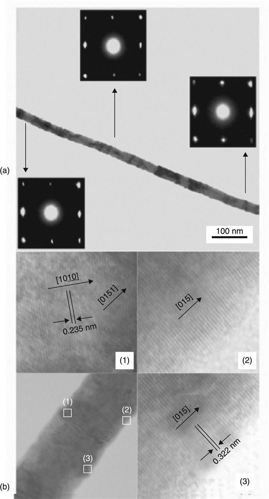
Han et al. (2011) reported that Bi2Te3 NWs obtained by electro-deposition on an aluminium membrane at room temperature had a rhombohedral crystalline structure. Similar NWs were deposited by pulsed electro-deposition with a diameter of 40 nm, equal to the pore size. These exhibited the preferred [015] direction (Fig. 6.22).
Ge-Sb phase change NWs without Te have been studied by Jung et al. (2009) and are of interest for their good data retention and fast switching properties. In particular, the two eutectic compositions of Ge-rich GeSb and Sb-rich Ge-Sb, with Sb ≥ 86%, can be achieved. For Sb-rich NWs, the expected structure was that of pure Sb, since they form a solid solution of Ge in Sb, with the Sb content varying between 0.86 and 0.90%. However, the structure determined by HR-TEM was that of hexagonal Sb, with growth direction along [012], where some stacking faults were also found, attributed to temperature accelerated growth kinetics. In the case of Ge-rich NWs, a tetragonal structure was obtained for single crystalline GeSb NWs growing along the [001] direction and exhibiting rectangular cross-sections, as observed by SEM.
Karthik et al. (2011) noted a threshold switching and negative resistance differential for Sb2SexS1 − x NWs, with diameter of approximately 30 to 150 nm, synthetized by a microwave-stimulated solvo-thermal synthesis technique. The structure of the single crystal NWs was orthorhombic, with the growth direction aligned along the high electron mobility one, namely [010].
Finally, the case of In-based NWs should be noted. Ahn et al. (2010) have obtained uniform, single crystal In3Sb1Te2 NWs with length 1 to 2 μm and diameter 50 to 70 nm. These NWs exhibited the expected fcc lattice structure. Sun et al. (2006) have shown that the single crystal In2Se3 NWs, with diameter of 40 to 80 nm and length up to 100 μm, exhibited the β-phase of the hexagonal lattice structure, with a growth direction along [110].
6.8 Conclusion
Different methods are being explored to obtain phase change nanowires to realize highly scaled memory devices. Although some technological obstacles have to be overcome, the chemical vapour deposition self assembly is one of the most studied, since it offers the possibility to realize peculiar NW geometries, compositional control and defect-free nanostructures.