Nanowire phase change memory (PCM) technologies: properties and performance
M. Longo, National Research Council, Italy
Abstract:
This chapter reviews key properties of nanowire (NW) phase change materials and how they affect device performance and reliability. Crystallization kinetics, phase transitions, thermal and electrical properties, as well as the properties of core-shell structures, are discussed. Size effects are considered, particularly in relation to scaling parameters, reduction of programming energy and drift resistance, since such effects can provide useful and sometimes unexpected properties with respect to other phase change memory (PCM) devices. A comparative analysis among high performing NW devices in terms of threshold voltage, programming currents and cyclability gives an idea of the strong potential of NWs when compared to conventional PCM devices.
Key words
nanowires; 1D structures; phase change memory; chalcogenide materials; functional analysis; nanoscaling; power consumption
7.1 Introduction
Scaling down phase change memory (PCM) cells from thin films to nanowires (NWs) requires solutions specific to each of the reliability problems introduced by the reduced length scale. As often occurs at the nanoscale, new physical effects, negligible at the larger length scale, have to be taken into account. This chapter reviews the main properties of nanowire phase change materials and how they affect device performance and reliability. It examines crystallization kinetics, phase transitions, and thermal and electrical properties, as well as the properties of core-shell structures.
7.2 Melting temperature and crystallization kinetics
One important mechanism in the phase change process is given by the crystalline → amorphous transition. In a NW we can introduce the melting temperature (or melting point) Tm, causing the disappearance of the associated electron diffraction patterns. As in the case of III-V semiconductor NWs, the downscaling in chalcogenide NWs implies a melting point depression. This has significant advantages for the amorphization (reset) currents, since the energy required to melt the material is reduced, provided that conventional melt-fast quenching is the actual mechanism occurring in NW amorphization. A reduction of the melting point in NWs is theoretically expected and can be expressed as a function of the NW diameter (D) by the formula (Li 2012):
[7.1]
where Svib(∞) is the bulk vibrational melting entropy; Tm(∞) is the bulk melting point; R is the ideal gas constant; and D0 is the critical radius at which almost all atoms of the particle are located on its surface.
Lee et al. (2008) performed in-situ TEM experiments to detect the diffraction pattern on single 80 nm wide GeTe and GST NWs. They discovered a 38% reduction of Tm for GST NWs and a 44% reduction of Tm for GeTe NWs. Analogous results collected from some other reports are summarized in Table 7.1.
Table 7.1
Effect of melting temperature reduction in different nanowires compared to their equivalent bulk materials
| Material | Tm bulk (°C) | Tm nanowire (°C) | Reference |
| GeTe | 725 | 410 | Lee et al. (2008) |
| 390 | Sun et al. (2007) | ||
| In2Se3 | 890 | 680 | Sun et al. (2006) |
| 722.5 | Jin et al. (2013) | ||
| Ge2Sb2Te5 | 616 | 375 | Lee et al. (2008) |
| Ge | 930 | 650 | Wu and Yang (2001) |

The phase transition modes of NWs also depend on material crystallization kinetics, in particular on the crystallization mechanism, related to the amorphous → crystalline state transition. For example, in bulk-like materials belonging to the GeTe-Sb2Te3 tie line, especially regarding the three stable phases Ge1Sb2Te4, Ge1Sb4Te7 and Ge2Sb2Te5, nucleation is the dominant mechanism over growth. It therefore results in a high crystallization temperature and low crystallization speed for alloys close to the GeTe composition, but in opposite properties in the case of alloys close to Sb2Te3. In materials such as Sb-rich Ge-Sb, Ge-doped Sb70Te30 or In-doped Sb70Te30, the growth of crystalline material from the amorphous regions dominates over nucleation. This gives high crystallization speeds, thermal stability and lower threshold voltages, but lower cyclability (Lacatita and Wouters 2008; van Pieterson et al. 2003).
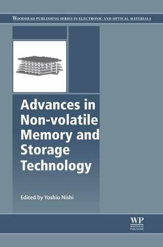
An important effect of their size observed in phase change NWs is related to the reduction of the writing (set) currents with NW dimensions. Lee et al. (2008) demonstrated this effect (Fig. 7.1) for PCM devices based on GeTe and Ge2Sb2Te5 NWs. Scaling down from 200 to 30 nm-thick NWs implied a current reduction from 3.70 to 0.43 mA for GeTe and from 1.31 to 0.15 mA for Ge2Sb2Te5 NWs. The power consumption was similarly reduced from approximately 6 mW to 0.63 mW for Ge2Sb2Te5 NWs. These effects could be interpreted as both being related to the increased heat localization and reduced melting temperature in diameter scaled NWs.
It is worth noting that the current and power reduction depends on material composition, which becomes a critical parameter in the switching behaviour of nano PCM cells. Yim et al. (2009) studied both the melting temperature reduction and sublimation effects in GeTe NWs coated with SiO2 layers. Their hypothesis was that the presence of the Au catalyst might affect the reduction of the melting temperature in a sort of reverse VLS mechanism. Hence they evaluated the vaporization coefficient of the NWs as α = 10− 3, which did not appear to depend on the NW diameter. Furthermore, they considered the sublimation of the remaining GeTe particles in the final stage of the NW sublimation without the Au seed and found that α is increased by up to 2 × 10− 2 when the GeTe nanoparticle is reduced to sufficiently small dimensions. This suggests an interesting parameter to consider in the evaluation of nanoscaled phase change devices.
The recrystallization of the amorphized state is instantaneously induced, as in the PCM operation mode, by heating the material using current pulses to a temperature above its crystallization temperature, but below its melting temperature, long enough to allow the structural rearrangement into the crystalline phase. Recrystallization kinetics influence the data retention capability of phase change NWs. Given that the crystalline state is the thermodynamically favoured phase over the amorphous one, there exists a time after which the amorphous phase is spontaneously transformed into the crystalline one at a given (even low) temperature. This essentially determines the thermal stability and thus the data retention time for a phase change NW. The recrystallization time, or data retention time, is defined as the time required by an amorphized phase change device to lose its stored information without any applied current pulse. This time can be calculated by studying the temporal evolution of the NW resistance, starting from the amorphized state and maintaining a fixed temperature within the system.
Lee et al. (2007) have examined the recrystallization times of GST NWs with different diameters (or thickness), by looking at amorphous → crystalline transformations occurring at 160 °C (Fig. 7.2(a)). The recrystallization time can be determined by the time at which the steep resistance drop occurs and it is evident that smaller NWs exhibited reduced crystallization times. Recrystallization is a thermally activated process, and thus related to an activation energy, Ea. The Arrhenius plots of recrystallization times as a function of 1/kT (k = Boltzman constant, T = absolute temperature) show a straight line, whose slope provides the Ea value for different NW diameters (Fig. 7.2(b)). Size also clearly had an effect, such that reducing the NW size implied reduced Ea values. However, all NWs are indefinitely stable at room temperature, with a data retention time of the order of approximately 4.8 × 10⁵ years for 30-nm NW-based devices.

A difficult consideration is the determination of the smallest NW size that can be favourably exploited to contemporarily obtain low programming currents and sufficient data retention. It must be taken into account that the operation mode of non-volatile memories can be required at higher temperatures, such as in automotive applications. Lee et al. (2007) reported that the data retention time changes from approximately 1800 years (Ea = 2.34 eV) for a 200 nm thick NW-based device operating at 80 °C, to approximately 3 years (Ea = 1.98 eV) for a 30-nm thick GST NW-based device at 80 °C.
The Ea data of Fig. 7.2(b) are plotted in Fig. 7.2(c) as a function of the NW thickness. By extrapolating the 20 nm thickness, a 1-year retention at 80 °C = 1.92 (Ea = 1.92 eV) was obtained, in turn corresponding to approximately 1.22 × 10⁵ years at room temperature. Such results reflect the importance of size effects in NWs for high performing PCM devices. This is particularly true of homogeneous and defect-free self-assembled structures, where the very low presence of compositional changes and structural or surface damage has little influence on the recrystallization process.
Li (2012) has derived some analytical equations, which do not require free parameters, to describe the behaviour of the crystallization activation energy Ea(D) and the nucleation rate N(D) in the amorphous phase for PCM nanomaterials, as a function of the characteristic dimension D, which corresponds to the diameter in the case of NWs. The model proposed was based on the theory of heterogeneous nucleation, in which surfaces, interfaces and defects catalyse the phase transition by lowering the energy barrier and increasing the transformation rate. This was found to fit well when compared with the experimental results in the case of Ge2Sb2Te5 NWs. Fig 7.3 shows a plot of the Ea(D) theoretical and experimental values. The corresponding decrease in Ea with the decrease in NW size was ascribed to the high surface-to-volume ratio in the NWs with low diameter, where surface atoms play an important role.

 (Lee et al. 2007) and
  (Lee et al. 2008) are experimental results. Reprinted from Li et al. (2012), copyright (2012), with permission from Elsevier.
The model is also useful for predicting the behaviour of the experimental N(D) values (Fig. 7.4). These increase as NW size decreases by 7 orders of magnitude from a 190 nm-thick to a 20 nm-thick NW. The dashed line results represent where the surface-to-volume effect was not considered. It predicts the trend, but is more distant from the experimental data. The N(D) size effect was attributed to both the increasing surface-to-volume effect and to the Ea(D) decrease.

 denotes the experimental results (Lee et al. 2008). Reprinted from Li et al. (2012), copyright (2012), with permission from Elsevier.
Khonic et al. (2000) showed that the Ea value is proportional to the crystallization temperature Tc, finding that Ea = CTc, where C is a size-independent constant. The reduction in Ea with the NW size reduction also indirectly indicates that the latter induces a thermal stability reduction. The opposite behaviour was observed in phase change films and nanoparticles with size < 10 nm. Caldwell et al. (2010) reported an increase in the crystallization temperature of GeTe nanoparticles from 320 °C (diameter = 3.4 nm) to 400 °C (diameter = 1.8 nm), at least 150 °C higher than the corresponding bulk value (170 °C). The enhanced amorphous phase stability of such nanoparticles was attributed to surface effects and to a lower surface energy of the amorphous phase than the crystalline one. Raoux et al. (2008) reported an increase in Tc in GeTe thin films deposited on SiO2 and capped in situ by 10 nm SiO2 and a decrease in melting temperature, Tm, with respect to the bulk values (Fig. 7.5).

It should be noted that data relating to the crystallization temperature of embedded phase change, ultra thin GST films with typical dimensions below 10 nm, can be affected by the presence of the matrix or cladding layers, inducing compressive stress capable of increasing the crystallization temperature (Simpson et al. 2010). Therefore the size effects of encapsulated chalcogenide nanostructures may exhibit different trends.
PCM devices are affected by a drift in the resistance and threshold voltage in time. The threshold voltage is the typical minimum voltage at which the structural phase change is induced, recalled more specifically in Section 7.5. Some ascribe this effect to compressive stress relaxation of the solidified amorphous phase (Karpov et al. 2007) and some to an intrinsic structural relaxation, reducing the defects of the amorphous phase after phase transition (Boniardi and Ielmini 2011). Mitra et al. (2010) investigated amorphous phase change GST NWs and found that, when the NWs have exposed free surfaces, their drift coefficients are extremely low in comparison to those of thin film devices. The drift of amorphous phase resistance, R, as a function of time, t, can be written as
[7.2]
The NWs exhibited a size-dependent resistance drift up to the thinnest 45 nm NW (Fig. 7.6). This size effect was again attributed to the high surface to volume ratio and exposed surfaces in the NWs. In fact, the presence of 300 nm dielectric films of SiO2 or Si3N4, embedding the NWs, induced stress effects which make the drift coefficients similar to those of thin film PCMs. The conclusion was that the built-in stress relaxation induced by the amorphization process is the major factor responsible for resistance drift.

Nanowire-like line cells have been proposed by Yoon et al. (2008). These are based on patterned nanoscale self-heating channels of Ge18Sb2Te5. The voltage necessary for cell reset was decreased from 4.2 V to 2.6 V, as the channel length was reduced from 500 to 100 nm, demonstrating the remarkable scaling effect on the power consumption. In summary, the list below gives the size effects that can be observed in phase change NWs:
7.3 Phase transition mechanisms
Surprising discoveries have been made by studying the structural transformations of phase change NWs in situ, during their phase transitions. Furthermore, this gives a rare opportunity to observe the phase change mechanisms, since similar studies in current PCM devices are difficult. This is because the active phase change material is confined by many layers of different materials, making it impossible to observe the device during operation, since its cross-section would be needed. Meister et al. (2008) have studied the structural transformations during the phase change in GeTe NW-based devices, with NW diameters in the range of 60 to 200 nm. Single Pt electrodes were placed on electron transparent silicon nitride membranes to allow direct in situ TEM observation. To switch them back and forth, the NWs were encapsulated in a 20 nm SiO2 sputtered layer. Figure 7.7 illustrates the results of the real-time TEM observation of phase transition under a voltage scan, correlating the structural and electrical analysis. Figure 7.7(a and b) shows the transformation towards the highly resistive state, starting from the deposited crystalline NW (with a two-point resistance of 3.7 kΩ). As the resistance was increased by the applied current, the surprising formation of nanovoids close to the contact regions was observed. The current maintained a preferential channel, due to the small shell of GeTe remaining on the SiO2 nanotube walls. The final resistance value was 42 kΩ, with a void length of about 1 μm. The reverse transition mechanisms also produced surprising results (Fig. 7.7(c and d)). Starting from a state of high resistance due to large voids in the NW, the voltage scan induced movement of the material, until the molten phase began, so that the shell tube could be refilled, resulting in removing the voids and restoring the initial NW resistance.

Void formation was therefore assumed to be the mechanism accounting for the very large measured resistance window, which was of the order of 107 between the on and off states. Notably, the molten material filling the voids was even observed to come from regions outside the contact areas. Structural transformations were observed in small regions of the NW, often located close to the contacts (due to the heat concentration for high contact resistance) or at necks in the NW, caused by switching. Rather than electro-migration, the possible dominant mechanism causing the motion of liquid GeTe was identified as the expansion due to material melting and overpressure in the SiO2 shell due to Te evaporation.
Jung et al. (2011) performed in situ HR-TEM observations of reversible phase transitions in proper PCM devices based on single GST NWs. They applied 50 ns voltage pulses with increasing amplitude and examined both the structural and electrical properties. A ‘notch’ structure was achieved for the NW suspended along the observation trench, in order to obtain a ‘hot spot’ in which the phase change was locally forced to occur, so that TEM analysis could be focused there. As well as full crystallization and full amorphization of the NWs, intermediate amorphous to crystalline transformations and vice versa were studied. Intermediate resistance states were reached by gradually increasing the voltage pulses. The case of HR-TEM analysis performed on partially recrystallized NWs should be noted, in which randomly oriented crystalline grains of approximately 5 to 7 nm were detected in the hot spot region, thus confirming a recrystallization mechanism dominated by nucleation.
The same group (Nam et al. 2012) have also examined the phase change transitions from crystalline to amorphous states in a similar single crystalline GST NW device, through in situ HR-TEM in real time. As in the previous case, GST NW-based PCM devices were suspended on proper 2 μm trenches. This allowed the TEM analysis under the application of a few 100 ns voltage pulses with increasing amplitude. After a time interval between pulses, which was sufficient to allow for device thermalization, the device resistance was measured. The first surprising result was that the NW resistance exhibited, while still in the crystalline state, a small decrease (‘resistance dip’) just before amorphization, after which an abrupt increase by two orders of magnitude occurred. This effect was observed in all NWs. Simultaneous HR-TEM observations with the appearance of the resistance dip allowed the identification of the presence of line defects in the form of dislocations. Such defects were characterized by a Burgers vector of ½ <11–20>, meaning that the dislocation loops are in the (10-10) prismatic plane of the hcp GST NW, growing along the [10-10] direction. Dislocations were observed to move aligned to hole (majority) carriers, and therefore under the influence of bias polarity. At the bottom of the resistance dip, the dislocations were stopped because of heavy accumulation, until amorphization took place. Amorphization was accompanied by a sharp resistance increase, with a bright line featuring the small amorphized region and a ‘cloud’ of dislocations left behind it. Further experiments were performed using the ‘notch’ structure and real-time HR-TEM observations during the crystalline → amorphous transition, in order to better localize the amorphized region. Analogous results were obtained (Fig. 7.8)

Starting from the fully crystalline NW, as it was grown in the notch zone (Fig. 7.8(a)), an initial dark region in the middle of the notch could be observed in Bright Field (BF) TEM images. This indicated the presence of strain (Fig. 7.8(b)). A contrast change was then observed, suggesting a motion from the positive to the negative electrode (Fig. 7.8(c)), followed by the sudden appearance of a bright line replacing the dark one (Fig. 7.8(d)). Dark Field (DF) TEM analysis clearly showed the presence of a cloud of dense dislocations (Fig. 7.8(e)), generated by the heat shocks of the voltage pulses in the monocrystalline NW, in which a vacancy condensation process occurs. The presence of electrical wind forces caused the dislocation motion. Thus, further vacancies were ‘consumed’, reducing the carrier scattering and decreasing the NW resistivity.
The generation, oriented motion and jamming of dislocations appeared to be the basis of the observed process in the studied GST NWs. However, the authors could not exclude the possibility that a form of transient melting occurs in the highly dislocated region before the resistance increase for amorphization.
7.4 Thermal properties
The phase transition between the reversible amorphous and the crystalline phase in PCM-NWs is based on the Joule heating effect induced by proper electrical pulses. Furthermore, we have shown that only a portion of the NW is involved in the structural change. The dynamics of the PCM cell are strongly related to heat dissipation. Therefore the thermal conduction properties in phase change NWs and the surrounding environment are important for understanding the device operation and reliability. The thermal analysis of nanostructured phase change systems, such as nanowires and related size effects, has not yet been explored in detail.
A molecular dynamics (MD) study conducted by Volz and Chen (1999) has demonstrated that the thermal conductivity of semiconductor NWs can be sensibly lowered with respect to bulk values (up to two orders of magnitude in the case of Si NWs), mainly due to phonon boundary scattering. It is therefore expected that in chalcogenide NWs a similar effect takes place, but also with advantages for heat localization and thus more efficient use of the transferred energy for phase switch. Heat localization in NWs caused by the Joule effect can be described in terms of the heat transport equation as (Piccione et al. 2013)
[7.3]
where k is the thermal conductivity of the NW; ρ is the electrical resistivity of the NW; r is the radius of the NW; and J is the current density = I/πr2. The writing current is given by
[7.4]
where ΔT = temperature variation between the transition temperature and room temperature. This equation shows the high impact of the NW size on the writing current. Reducing thermal conductivity lowers the writing currents, along with the decrease of the maximum temperature that is reached in the ‘hot spot’ of the NW.
A compact model was presented by Chen and Pop (2009), in order to examine the temperature distribution in cylindrical PCM-GST NWs. This model solves the heat diffusion equation, taking into account the effect of thermal boundary resistance (TBR) at the interfaces formed by the contact area between the NW and the TiN electrodes, as well as the NW sidewalls and the SiO2 embedding matrix (Chen and Pop 2009; Zuev et al. 2010). The model analyses the programming current dependence on geometric properties. We focus here on the dependence of programming current on the material properties (Fig. 7.9). It is interesting to note that, if the thermal conductivity of the materials is lowered, the programming current is reduced, due to better thermal confinement. Similar results were obtained for thin film-based PCM devices (Reifenberg et al. 2008). The model also agreed well with the finite elements (FE) simulation. Better thermal confinement was obtained by higher TBR values, with the effect of reducing the programming current by up to a factor 3. Finally, Fig. 7.9 shows how the increase of the GST electrical resistivity lowers the programming current, since it is intrinsically related to the thermal conductivity.

Jin et al. (2013) have studied the size dependence of the thermal resistance in In2Se3-based phase change NW PCM devices. The NWs had a diameter in the range of 60 to 200 nm and were encapsulated in a 400 nm thick SiO2 layer. The thermal resistance as a function of the NW diameter was investigated on the basis of the programming power, Pprog, measurement and the transition temperatures TC (Ts for crystallization and Tr for amorphization). By integrating the Fourier equation along the heat flux direction, the following relation was established:
[7.5]
where RTh is the NW thermal resistance and T298K is the thermal chuck temperature. The Wiedemann-Franz law was then applied:
[7.6]
where k is the thermal conductivity, σ is the electrical conductivity and L is the Lorentz number = 2.44 × 10− 8 W Ω K− 2. By using this, it was possible to correlate the electrical resistance (Re) and thermal resistance (RTh) of the amorphous (A) and crystalline (C) phases:
[7.7]
The results produced by the above calculation are shown in Fig. 7.10, for the thermal resistance and power consumption of the NWs as a function of the NW diameter.

Notably, the thermal resistance (and the related power consumption) exhibited a size dependence and a tendency to increase (and power consumption to decrease) when the NW diameter was lowered in amorphous and crystalline In2Sb3 NWs. In this case, the thermal resistance ratio between the NW and bulk phase was around 105 for the amorphous and around 10 for the crystalline phase.
In PCM operation, undesired ‘proximity disturbance’ effects are related to ‘thermal cross-talk’, which is the probability that the heat generated by a programmed cell can be propagated to a non-programmed adjacent cell. This has the effect of destroying the correct information and storing incorrect data encoding (Lacaita 2006). The problem can also affect NW-based PCM devices. An analytical model for isotropic downscaling of phase change NW size by a factor of 1/k (k > 1) showed that the thermal crosstalk effect is reduced in NWs. The operation speed is increased by a factor k2 and the programming current is reduced by at least a factor k3, demonstrating a further advantage of phase change NWs (Liu et al. 2011). We can summarize the effects of employing phase change NWs, in comparison with their corresponding bulk materials, in the following points:
The combination of the resulting transition temperature reduction (Section 7.2), reduced thermal conductivity and reduced volume to be programmed, makes the phase change NW a very efficient, low power consuming PCM cell.
7.5 Electrical properties
The configuration used to measure the electrical properties of phase change NWs is given by the NWs contacted through proper electrodes as single nanocells, often horizontally placed on an insulating substrate (typically SiO2). Metallization is usually brought about by using Focused Ion Beam (FIB) techniques, coupled with nanolithography to achieve a whole circuit, up to the macro pads. The single NW can be exposed to air, with the effect that oxidation and material evaporation rapidly degrade the nanocell and very few switching cycles are possible. In order to avoid this problem, the NW can be encapsulated in a proper dielectric material. Ideally, a regular array of vertical NWs buried in a dielectric matrix is obtained, which allows the deposition of the contacts at the NW ends, thus yielding collective information on a large number of nanocells (Han et al. 2011).
The electrical characterization of phase change NWs uses the study of the electrically-triggered transition of the material from the amorphous (RESET, high resistance) to the crystalline (SET, low resistance) phase and vice-versa. The pulsed I/V (current vs voltage) technique is widely employed, in a similar way as it is used in conventional PCM devices. The resulting measurement can be used to determine the threshold voltage of the device, Vth. This parameter is very important from a technological point of view, because it represents the minimum voltage required for the operation of the nanowire PCM device (Lacatta and Wonters 2008).
The amorphization of the nanowire devices (RESET) is achieved by an intense, short voltage pulse, which is believed to rapidly melt and quench a portion of the nonowire. Crystallization (SET) is achieved by a less intense, but longer voltage pulse, which triggers a more complex process. Firstly, the increase of the electric field across the amorphous region causes the density of charge carriers to increase, due to inelastic scattering. As a result, the resistance of the amorphous chalcogenide decreases, which means that there is sufficient current flow to heat the material above the crystallization temperature by the Joule effect (Pirovano et al. 2004).
The electrical analysis for NW-based PCM devices is intended to determine the same performance indicators as are used for PCM cells, as listed below (essentially depending on the phase change material properties):
• set and reset currents: reset current is the highest current needed to allow the cell operation, and is thus directly related to the cell power consumption;
• electrical resistance: of the cell in the high conductivity (set) and low conductivity (reset) states;
• programming window: namely the resistance gap between the set and reset state. A programming window of at least two orders of magnitude is required for the proper operation of the device, to prevent ambiguities in the cell status data reading;
• the number of switching cycles: capable of keeping the width of the programming window constant, also defined as ‘endurance’;
• the threshold voltage: required for amorphization;
• the data retention time: related to the retention of the amorphous phase (RESET) state (as explained previously); the conventional requirement for non-volatile storage is a retention > 10 years at 85 °C.
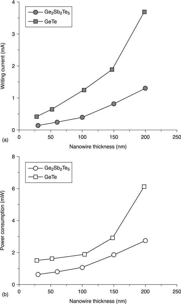
In order to program a NW cell, appropriate values for the voltage pulses have to be selected by considering the programming curve, which is the plot of the cell resistance (R) value as a function of the voltage pulse amplitude. This analysis provides the set (Vset) and reset (Vreset) voltage values (generally a few V), once the duration of the pulses has been selected (on the scale of hundreds of ns, necessary to transfer enough energy for crystallization). In Fig. 7.11 (Lee et al. 2008), the pulsed I-V (a) characteristics under a voltage sweeping and R-I programming curves (b) are reported for GeTe and GST NW devices (NW thickness = 100 nm). The NWs deposited were single crystalline and the corresponding I-V curve in Fig. 7.11(a) shows a linear dependence. In the amorphous to crystalline transition under increasing voltage pulses, the Vth was evident at 0.8 V for GeTe and 1.2 V for GST, after which the crystallization of the two materials was gradually completed.
Subsequently, the system returned to its initial situation and another cycle could be performed, indicating the reversibility of this process. The R-I programming curve in Fig. 7.11(b) showed how the current pulses of different amplitude could selectively induce either the crystallization or the amorphization of the phase change material. This in turn determines a crystalline state resistance at approximately 1.5 kΩ for GeTe and approximately 17 kΩ for GST and an amorphous state resistance of 3.8 MΩ for GeTe and 1.58 MΩ for GST. A minimum current amplitude of approximately 1.2 mA for 100 ns was necessary to start the amorphization of GeTe NWs, as opposed to that required for GST of 0.24 mA for 300 ns. GST NWs therefore created memory devices with a higher threshold voltage, but a lower current consumption needed to achieve crystallization, when compared with GeTe NW-based devices. However, GeTe NW devices provided a larger programming window.
Resistance-voltage (R-V) curves were used to evaluate the operating voltage for a PCM cell based on In2Se3 NWs, with and without an SiO2 passivating layer of 400 nm. Results for this have been reported by Baek et al. (2013). By applying increasing voltage pulses, while maintaining pulse duration in all experiments (100 μs for set and 200 ns for reset), the results shown in Fig. 7.12 were obtained.

In the presence of a SiO2 passivating layer,the values of Vset decreased from 6 to 3.8 V and Vreset from 8 to 4.8 V, when the programming window was approximately 2.5 × 10⁵. This showed a 40% reduction in the programming voltage, and a 27% reduction in the programming power. This effect was attributed to the reduced heat loss from the passivated NWs to the surroundings.
Longo et al. (2012) have analysed a Ge1Sb2Te4 NW-based PCM device, for which the SEM image is shown in Fig. 7.12. The single NW (80 nm thick, 1 μm long) was contacted using FIB-Pt contacts touching the aluminium pads to pick up the signal. In Fig. 7.12(b), the I-V characteristics are shown for the device. The NW was deposited as crystalline, with approximately 6 kΩ resistance. A threshold switching value of 1.35 V was recorded for amorphization, lower than in thin film devices based on Ge1Sb2Te4 (1.41 V). The amorphized NW state exhibited a resistance of approximately 450 kΩ and thus a programming window of about 102, which is smaller than in Ge2Sb2Te5 NWs. The corresponding values from a 60 nm GST NW (Longo et al. 2012) are also shown in Fig. 7.13, as a comparison. The device could only be reversibly switched 9 times, which is much fewer than the 105 write/rewrite cycles reported in Lee et al. (2007) for GST NWs. However, the Ge1Sb2Te4 NWs were not embedded and so were exposed to air during cycling, meaning that oxidation and evaporation quickly degraded the test device during operation. With regard to cycling switching, it is also interesting to consider the results obtained by Fallica et al. (2011) for a PCM device based on a single GeTe NW (60 nm thick, 2 μm long). The device resistance behaviour in Fig. 7.14 shows that the GeTe nanowire as deposited was initially in the cubic phase, a conclusion also supported by structural analysis using HR-TEM. The initial resistance was around 60 kΩ. After the first pulse, the resistance increased to 90 MΩ, indicating the NW amorphization. Crystallization pulses brought the wire into the (more conductive) rhombohedral phase and the corresponding resistance dropped to 10 kΩ. It was not possible to revert back to the cubic phase. As the NW was not passivated, after ten switching cycles no more phase changes were observed.


Jung et al. (2009) have reported on memory switching in Ge-Sb NWs with two different eutectic compositions: (i) Sb-rich Ge-Sb (Sb > 86 at%); and (ii) Ge-rich GeSb. Electrical analysis was performed by examining their I-V, R-V and cyclability curves. For 80 nm thick Sb-rich Ge-Sb NWs, the switching behaviour could be obtained with a Vth of approximately 4 V. However, after the first crystallization sweep, the initial resistance value of approximately 36 kΩ was not recovered, but set to higher values. Similar results were obtained for NWs up to 120 nm in thickness, indicating that electrical reversibility was not complete. TEM results suggested that the partial irreversibility was due to phase separation of Ge under thermal annealing. Analogous electrical measurements performed on Ge-rich Ge-Sb NWs did not show any switching behaviour.
The effect of Bi-doping (~ 3 at.%) on the electrical properties of GeTe NWs has been studied by Zhang et al. (2013). This constitutes one of a very few examples of NW-doping. The analysis of the I-V characteristics showed an increase in the set and reset resistances of around two orders of magnitude and the programming currents were decreased with respect to the undoped material. Furthermore, the crystallization time was reduced by a factor of 20.
Finally, an extremely low reset current in very small GST NWs, 40 nm wide and approximately 10 nm long, was accomplished in a nanogap aligned to CNT electrodes, with a contact area of a few nm2. A 10 nm passivating layer of SiO2 was also deposited. The I-V and R-I curves in Plate V (see colour section between pp. 268 and 269) show that the threshold switches between the reset state at 2.5 GΩ resistivity and the set state at 1.3 MΩ. After the first amorphization, the threshold voltage value fell by 20 to 30%, until it was stabilized at lower values of approximately 3.2 V, after 100 switches. The set current was approximately 0.4 μA and the reset current approximately 1.9 μA, which constitute the smallest values ever reached. The programming window was approximately 2 × 10³ and around 1500 switching cycles were demonstrated. Since early attempts, NW devices have shown a power reduction of 1 to 2 orders of magnitude, when compared to conventional thin film PCMs (Lee et al. 2008). Table 7.2 summarizes the main electrical properties of phase change NW-based PCM devices, compared with equivalent devices based on planar and confined cells. The potentialities of the NWs in terms of the programming window and programming currents can be seen.
Table 7.2
Comparison of the main electrical switch properties in chalcogenide NW and planar/confined PCM devices. NA = Not Available
| Material and NW diameter (D) | Set resistance (Ω) | Reset resistance (Ω) | Switching cycles | Programming current | Threshold voltage (V) | Reference |
| GeTe NW, D = 60 nm | 104 | 108 | 10 | NA | 0.7 | Fallica et al. (2011) |
| GeTe NW, D = 100 nm | 2 × 10³ | ~ 4 × 10⁶ | NA | ~ 0.5 mA for set, | 0.8 | Lee et al. (2008) |
| ~ 1.5 mA for reset* | ||||||
| GST NW, D = 100 nm | ≈ 104 | ~ 2 × 10⁶ | NA | ~ 0.24 mA for set, | 1.2 | Lee et al. (2008) |
| ≈ 104 | 1.8 × 10⁶ | > 105 | ~ 0.45 mA for reset* | 1.8 | Lee et al. (2007) | |
| GST NW, D = 60 nm | 0.25 mA for set | |||||
| Ge1Sb2Te4 NWs, D = 80 nm | 1.4 × 10⁴ | 4.5 × 10⁵ | 9 | NA | 1.35 | Longo et al. (2012) |
| Ge0.2Sb3Te6.8 NWs, 50 nm | 1.4 × 10⁴ | 9.10 × 10⁶ | A few | NA | NA | Longo et al. (2013) |
| GST NW, in a nanogap aligned to CNT, D = 40 nm + SiO2 passivation | ~ 1 × 10⁶ | ~ 7 × 10⁹ | > 103 | 0.1 μA for set, 1.6 μA for reset | 3.2 | Xiong et al. (2013) |
| In2Se3 NWs, D = 100–350 nm No NW passivation |
6.57 × 10⁴ | 1.5 × 10¹⁰ | > 10 | NA | NA | Baek et al. (2013) |
| In2Se3 NWs, D = 100–350 nm + SiO2 passivation | 3.25 × 10⁴ | 8.3 × 10⁹ | > 20 | NA | NA | Baek et al. (2013) |
| Sb2Te3 NWs, D = 99 nm | ~ 28.9 × 10³ | ~ 28 × 106 | 10 | NA | 0.75 | Lee et al. (2008) |
| Bi2Te3 NW, array | ~ 2.3 × 10³ | ~ 2 × 10⁷ | ≈ 50 | NA | 1.2 | Han et al. (2011) |
| Bi2Te3 NW, single | 0.6 × 10³ | 7.5 × 10⁶ | NA | NA | ≈ 0.35 | Han et al. (2011) |
| Ge-Sb NWs, D = 70–100 nm | ~ 1 × 10⁵ | ~ 4 × 10⁶ | 200 | 0.24 mA for set | 4 | Jung et al. (2009) |
| In3Sb1Te2, D = 70 nm | ~ 1 × 10⁸ | 5 × 10⁹ | NA | NA | 1.6 | Ahn et al. (2010) |
| Sb2Te line memory cell | ~ 1 × 10⁴ | ~ 5 × 10⁶ | 107 | 280 μA | NA | Jedema et al. (2008) |
| Doped Ge-Sb bridge cell | ~ 3 × 10⁴ | ~ 4 × 10⁵ | > 104 | 60 μA for set 90 μA for reset |
~ 1 | Chen et al. (2006) |
| GST NW by electron beam lithography - width 39 nm | ~ 1 × 10⁴ | ~ 1 × 10⁷ | NA | 2 μA for set | 1.81 | Ma et al. (2011) |
| GST planar cell | ~ 5 × 10³ | ~ 1 × 10⁶ | 1012 | ~ 100 μA for set, ~ 700 μA for reset | 0.6 | Lacaita and Wouters (2008) |
| 7.5 nm dash-type confined PCM cell | Programming window circa 1 order of magnitude | 2 × 10¹⁰ | 160 μA for reset | 0.65 | In et al. (2008) | |
| Lateral PCM/CNT | ~ 2 × 10⁶ | ~ 5 × 10⁷ | 200 | 1 μA for set, 5 μA for reset | 3.5 | Xiaong et al. (2011) |
| GeTe cross-point PCM with CNT electrodes | ~ 2 × 10⁶ | ~ 2 × 10⁷ | > 100 | 1.4 μA for reset | 5–13 | Caldwell et al. (2012) |
| 45 nm Microtrench GST PCM cell (Numonyx) | ~ 1 × 10⁴ | 2 × 10⁶ | > 108 | 200 μA for reset | NA | Servalli (2009) |
| Cross spacer | 1 × 10⁴ | 2 × 10⁵ | > 106 | 230 μA | NA | Chen et al. (2007) |
| Interfacial PCM | ~ 1 × 10⁴ | ~ 1.5 × 10⁶ | > 107 | ~ 0.2 mA for set, ~ 0.6 mA for reset | NA | Simpson et al. (2011) |

*Estimated values.
7.6 Properties of core-shell structures
In the case of designing multilevel cell (MLC) storage, which would considerably increase data storage density, double layers of GST and Sb2Te3 were considered (Rao et al. 2007). Endurance was measured for up to 105 programming cycles. Due to the very close melting temperatures of the two alloys, severe inter-diffusion occurs during the reset process. This limits the stability of the middle resistance level. Improved performances were reached by intercalating a TiN layer between Sb2Te3 and GST (Rao et al. 2009). Higher endurance was therefore possible. However, due to the low thermal conductivity of TiN, more heat was dissipated within the cell, and higher reset voltages were required so that increased power consumption was necessary. Multilevel data storage was also investigated using the In3SbTe2 compound, which provided four different resistance levels, enabled by the distinct crystallization of the binary InSb and InTe compounds (Kim et al. 2011). Multilevel data storage based on core-shell NWs has been investigated in a highly original study by Jung et al. (2008), by using a GST (core) and GeTe (shell). Three different resistance levels were resolved in the R-I characteristics, with two slightly different middle resistance states, corresponding to the core chalcogenide material in the amorphous phase and the shell material in the crystalline phase or vice versa, although information relating to their endurance is not available. It must be noted that this kind of structure, obtained by self-assembly CVD technique, cannot be obtained through lithography based processes.
Programming could be performed by acting on the crystalline/amorphous phases of the involved materials in order to exploit low programming volumes, high cell density and defect-free nanostructures. Multilevel data ‘0’, ‘1’ and ‘2’ encoding was achieved by introducing different offsets of phase transitions, in a core-shell/shell-core sequence. This made it possible to obtain at least an intermediate, mixed resistive state, between the high and low resistive states of the core and shell materials (Figs 7.15(a,b)). Finally, it is worth noting that only a few patents have been submitted for the use of chalcogenide-based NWs for memory applications (Elmegreen et al. 2011; Yoon et al. 2011; Wong et al. 2011). None of these directly deals with the use of core-shell NWs.


7.7 Conclusion
Given the possibility that even core-shell structures can be implemented and that proper combinations of Ge-based and In-based NWs can be employed, the performances shown in Table 7.3 can reasonably be expected for future phase change NW-based PCM devices. Moreover, the estimation of a cost reduction by a factor of 2 with respect to the current PCM devices could in fact be attained, if the MLC core-shell NW option is achieved.
Table 7.3
Expected performances for future NW-PCM devices
| Property | PCM state-of-the-art | NW-based PCM |
| Power consumption | 50 pJ/bit | 5 × reduction |
| Scalability | 45 nm demonstrated | 10 nm litho node |
| Density | 20 Gbits/sq.in. | 5 Tbits/sq.in. |
| Programming time | 100 ns | 80 ns |
| Stability | 10 years at 85 °C | 10 years at 85 °C |
| Endurance | > 106 | > 106 |
Phase change NWs are fundamental to exploring future non-volatile memory devices. They can be employed in highly scalable, low-power, high speed and high density devices. Furthermore, their size-dependent properties can be used, coupled with the control of their compositional and structural properties. This should bring the PCM technology well beyond the limitations of current Flash devices, which rely on charge trapping.
At the same time, phase change NWs pose important challenges with regard to their technological implementation into PCM devices. Many approaches are being considered, both involving top-down and bottom-up or indeed mixed techniques and also employing carbon nanotubes. While lithography-based methods can result in compatibility with CMOS technology, bottom-up methods can lead to dense and defect-free NWs, with the further benefit of providing an ideal means to study intrinsic nanostructure properties and size effects. It is likely that a mix of the above approaches will be necessary in future. As for the mass production target, the MOCVD technology for the synthesis of phase change NWs should be highlighted. It is characterized by high process control and large area deposition, thus allowing the potential for relatively easy industrial transfer.
7.8 Acknowledgement
The author would like to acknowledge the fruitful scientific discussions with R. Fallica of IMM-CNR, Laboratorio MDM, Agrate Brianza, Italy.