Phase change memory (PCM) materials and devices
S. Raoux and T.J. Ibm, Watson Research Center, USA
Abstract:
This chapter first discusses the unique properties of phase change materials including the structure of the amorphous and crystalline phases as well as their optical, electrical and scaling properties. Then the principles of phase change memory (PCM) are described, including device characteristics, cell concepts and design, advanced prototype devices and scaling and process integration. We include a review on materials engineering for PCM and shows how materials can be optimized for various PCM applications. Finally, an outlook is given and new applications of phase change materials, such as such as logic and neuromorphic computing, are discussed.
Key words
phase change materials; phase change memory; material design; device fabrication; process integration
5.1 Introduction
Ovshinsky (1968) described two kinds of switching mechanisms observed in chalcogenide alloys, threshold switching and memory switching. Threshold switching is the sudden drop in resistance of an amorphous chalcogenide alloy (composed of 48 at.% Te, 30 at.% As, 12 at.% Si and 10 at.% Ge) when it is located between two electrodes and a certain applied voltage is surpassed. This resistance drop, which is an electronic effect, is reversible if the voltage is removed fast enough and the alloy returns to a high resistance, amorphous state. Memory switching, in contrast, is the reduction in resistance that remains after the voltage is removed. This was observed in a different alloy with the As fraction reduced to 5 at.% and is caused by a change in the phase of the chalcogenide from the highly resistive amorphous phase to the conductive crystalline phase induced by Joule heating. However, it is possible to return from such a crystalline, conductive state to the amorphous, resistive phase by melting and very rapid cooling (melt-quenching), and this reversible switching between the two phases is the base of phase change memory (PCM).
It was also discovered soon after that such a phase change can be produced not only by Joule heating but also by laser heating, and that the two phases are characterized by a large difference in optical properties (Feinleib 1971). This is the base of rewritable optical storage using phase change materials and a detailed description of this technology can be found in Meinders et al. (2006), Shi (2009), Tominaga (2009) and Yamada (2009).
Early phase change alloys were characterized by relatively long crystallization times and it took the breakthrough discovery by Yamada et al. (1987) of fast switching alloys on the pseudo-binary line between GeTe and Sb2Te3, most notably Ge2Sb2Te5, to develop the highly successful rewritable optical storage technology, and to renew the interest in PCM.
This chapter will first introduce phase change materials with their unique combination of properties, then describe aspects of PCM, including device characteristics and materials engineering for PCM, and finally indicate new potential applications of phase change materials, not in memory but in logic and neuromorphic computing.
5.2 Phase change materials: structure and crystallization kinetics
5.2.1 Structure of amorphous and crystalline phase change materials
Phase change materials are materials that exist in an amorphous phase and in a crystalline phase. In this sense, almost any material is a phase change material. However, to be a technologically useful, phase change material (and this is how the term ‘phase change material’ is applied in the literature) needs to fulfill a number of properties that depend on the specific application. Since the first commercial application of phase change materials was in the rewritable optical data storage phase, change materials were optimized with respect to their optical properties such as strong optical contrast at the required wavelength. For PCM, other material properties are important and a different material optimization is required. Table 5.1 summarizes the relevant phase change material properties and how they influence PCM performance (Wuttig and Raoux 2012).
Table 5.1
Phase change material properties and their effect on PCM performance
| Material property | Desired value | PCM performance |
| Melting temperature | Low | Reset current will be lower for low melting point materials |
| Crystallization temperature | Relatively high | Data retention is improved |
| Thermal conductivity | Low | Better heat confinement, reduced switching currents |
| Activation energy for crystallization | High | Improved archival lifetime, data retention |
| Resistance (crystalline) | Relatively high | Reduced reset current, improved cyclabiliy |
| Resistance (amorphous) | Relatively high | Increased on/off ratio, improved cyclabiliy |
| Resistance levels | Stable | Multilevel operation possible |
| Crystallization speed | High | Data-rate increased |
| Threshold field | Depends on cell size | Will need to be increased for smaller cells to avoid cell switching with reading pulse |
| Chemical stability | High | Increased cycle numbers without elemental segregation |
| Mass density | Little change between phases | Reduced void formation |
Source: Reprinted with permission from Wuttig and Raoux (2012). Copyright © 2012 WILEY-VCH Verlag GmbH & Co. KGaA, Weinheim.
Fast crystallizing phase change materials with large optical and electrical contrast are found to have resonant bonding characteristics in the crystalline phase and covalent bonding in the amorphous phase. For resonant bonding to occur in inorganic solids, ionicity needs to be relatively low and hybridization of the s- and p-valence electrons needs to be relatively weak (Shportko et al. 2008). These conditions are fulfilled for many tellurides, for example GeTe and Sb2Te3. Fast crystallizing phase change materials are also characterized by a highly symmetrical, cubic or rock-salt crystalline structure, such as the metastable crystalline phase of Ge2Sb2Te5.
Phase change materials possess a large amount of vacancies, and for some materials the vacancy concentration can reach 20% (Yamada and Matsunaga 2000). By using density-functional theory, it was shown that the most stable crystalline phase in Ge-Sb-Te alloys can be obtained for distorted rock-salt like structures with large vacancy concentrations (Wuttig et al. 2007). Energetically unfavorable anti-bonding Ge-Te and Sb-Te states are annihilated by vacancy formation and this contributes to a higher stability of the crystalline phase with high vacancy concentrations. Many phase change materials of the Ge-Sb-Te system, such as Ge1Sb4Te7, Ge1Sb2Te4, Ge2Sb2Te5 and Ge3Sb2Te6, exhibit in addition to the amorphous-crystalline phase transition a metal-insulator transition upon further annealing (Siegrist et al. 2011). If these initially amorphous alloys are heated, they show a negative temperature coefficient of resistivity as expected for an insulator. When the crystallization temperature is reached, the resistivity is suddenly decreased, caused by the amorphous-crystalline phase transition. However, the crystalline phase still shows a negative temperature coefficient of resistivity. Only upon further annealing to higher temperatures, when a critical resistivity of about 2 to 3 mΩ cm is reached, the behavior changes from non-metallic (negative temperature coefficient of resistivity) to metallic behavior (positive temperature coefficient of resistivity). This metal-insulator transition has recently been explained using density functional theory, indicating the ordering of vacancies being responsible for the metal-insulator transition (Zhang et al. 2012).
5.2.2 Crystallization kinetics
The crystallization of the amorphous phase change material is the process that determines the data rate in PCM. Relatively long crystallization times of early phase change alloys prevented PCM technology from being viable from the 1970s to the 1990s. The understanding of the crystallization process is thus of great importance to the development of novel phase change materials. The classical theory of crystallization involves two processes, namely crystal nucleation and crystal growth. Nucleation is called homogeneous nucleation if it occurs in the interior of the amorphous phase. However, nucleation can occur at impurities or at interfaces, and in this case is called heterogeneous nucleation, where atoms are attached or detached from a crystalline cluster by thermodynamic fluctuations. The equilibrium size distribution of clusters is determined by Boltzmann statistics and is given by (Landau and Lifschitz 1969)
[5.1]
where Nequ(r) is the number of clusters of radius r at equilibrium, N0 is the total number of atoms in the amorphous phase, ΔGcluster(r) is the reversible work for crystal cluster formation, kB is the Boltzmann constant, and T is the absolute temperature. ΔGcluster(r) is determined by the interplay of the Gibbs free energy difference between the amorphous and the crystalline phase per unit volume, ΔGac, and the energy term resulting from the creation of an interface between the crystalline cluster and the amorphous phase. It can be expressed as (Christian 1975)
[5.2]
where σ is the interfacial free energy. Figure 5.1 depicts the reversible work for crystal cluster formation, ΔGcluster(r), as a function of cluster radius. It has a maximum at the so-called critical cluster radius rc given by
[5.3]

and the reversible work for critical crystal cluster formation ΔGc(rc) is
[5.4]
Clusters that are smaller than rc are energetically unfavorable and decay, and clusters that are larger than rc grow due to a gain in free energy ΔGc(rc) and can be considered the activation energy for crystallization. For heterogeneous nucleation at an interface, for example on a substrate, Eq. 5.4 is modified by a geometry factor that depends on the wetting angle between the crystal nucleus and the substrate (Vollmer 1929). Which type of nucleation dominates is determined by the relative values of crystal-substrate, crystal-amorphous and amorphous-substrate interfacial energies. In phase change alloys, the crystallization is diffusion-limited (compared to the collision-dominated process for nucleation from a gas phase) and the steady-state nucleation rate Iss can be estimated by
[5.5]
where η is the numerical value of the liquid shear viscosity in units of poise (1 poise = 0.1 Pa s). A detailed description of phase change materials crystallization kinetics can be found in Kalb (2009).
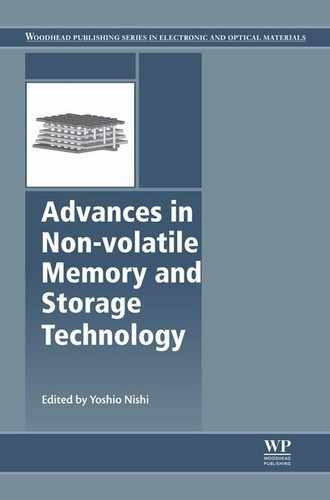
In phase change materials, crystal growth occurs at the amorphous-crystalline interface of supercritical nuclei by atomic rearrangements. Regarding the relative role of nucleation and growth, phase change materials are often categorized into nucleation-dominated and growth-dominated materials. Figure 5.2 shows atomic force microscopy (AFM) images of two different amorphous phase change materials, Ge2Sb2Te5 and Ge:Sb = 15:85 (in at.%), after exposure to laser pulses attempting crystallization. Since the crystalline phase has a higher mass density than the amorphous phase for these materials, crystalline areas appear dark (lower). It can be clearly seen that for Ge2Sb2Te5, many small crystals are formed within the laser spot, indicative of a high nucleation rate, and these crystals then grow slowly (nucleation-dominated material). However, for Ge:Sb = 15:85, only one nucleation site occurs for each laser spot from which the crystal then grows rapidly (growth-dominated material). Nucleation rate and growth velocity show temperature-dependent maxima between the crystallization temperature Tx and the melting temperature Tm, with the maximum for the growth velocity typically at a higher temperature than the maximum for Iss. Therefore, the same material can appear to have nucleation-dominated crystallization at lower temperature and growth-dominated crystallization at higher temperature. Evidence for this was observed, for example, in In- and Ag-doped Sb2Te3 (Raoux et al. 2008a; Raoux 2009).
Nucleation rates and crystal growth velocities are strong functions of temperature and span many orders of magnitude (Santala et al. 2013). This enables PCM technology because the same material can be stable in the amorphous phase at room temperatures for decades or even years, but it can crystallize within nanoseconds at elevated temperatures. A difference in response time of 1017 was estimated by Yamada (2009). This underlines again the unique combination of properties of phase change materials.
5.3 Properties of phase change materials
5.3.1 Optical and electrical properties of phase change materials
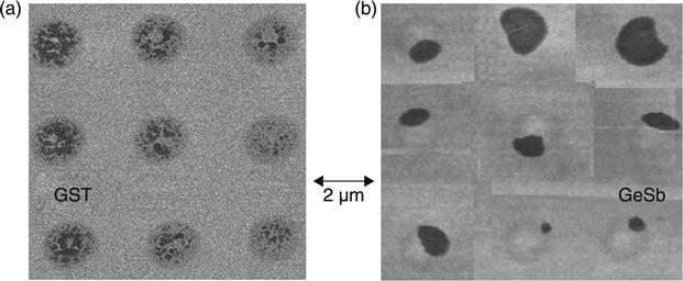
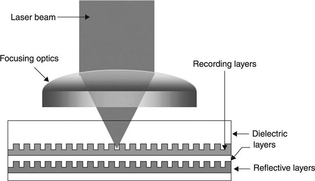
The first technological application of phase change materials in rewritable optical storage discs is based on the different optical properties of the amorphous and crystalline phases. Optical discs consist of a substrate, one or more recording layers of phase change material sandwiched between dielectric layers (typically ZnS-SiO2) for mechanical protection, and a reflective layer. Figure 5.3 shows a schematic of such a disc. The crenellated shape of the recording layers helps to isolate adjacent tracks. Optical recording requires strong optical contrast at the wavelength used. Figure 5.4 shows the optical constants n, k and the absorption coefficient α as a function of wavelength λ for Ge2Sb2Te5 (Lee et al. 2005; Lee and Bishop 2009). Also indicated are the wavelengths at which rewritable CDs, DVDs and Blu-ray discs operate. It is clear that the optical constants change significantly with wavelength, and storage material optimization is required for each wavelength. The third-generation product, the Blu-ray disc operating at 405 nm laser wavelength, utilizes a phase change material much closer to GeTe on the GeTe-Sb2Te3 pseudo-binary line compared to alloys used in rewritable CDs, which required good optical contrast and large absorption in the infrared (780 nm).


Often static laser testers are used to evaluate the optical properties of phase change materials. Such a tester in many cases consists of two lasers, one pulsed high power laser to heat the sample and induce phase transformations, and one low power laser to measure reflectivity. Various experiments can be performed with such a test to characterize a phase change material with fast turn around time and without the need for fabricating PCM devices. The easiest experiment exposes a thin film of phase change material to pump laser pulses of variable power and duration, and measures reflectivity before and after the pump pulse. Crystallization occurs for laser power and duration above a certain threshold when the crystallization temperature is reached in the laser spot, and is evidenced by an increase in reflectivity. The crystallized areas will appear as bright spots in an optical microscope image.
Most phase change materials have a higher reflectivity in the crystalline phase compared to the amorphous phase, but there are some exceptions, for example GaSb (Cheng et al. 2011a) or GeCu2Te3 (Saito et al. 2013). By determining the pump laser pulse length required for crystallization, we can measure crystallization speed. In another experiment, the phase change material is first crystallized either by annealing in a furnace, by depositing the film above its crystallization temperature, or by scanning the pulse laser over the sample, which can create a crystalline area at the correct pump laser power.
When such a crystalline film of phase change material is exposed to pump laser pulses of variable power and duration, the laser pulse produces dark marks in the bright film, a negative optical contrast indicating successful melt-quenching of the crystalline film to create amorphous marks. The ultimate test for the technological usefulness of a material is the re-crystallization of amorphous marks in the crystalline film, because in optical discs the data is stored as amorphous marks in crystalline film. In this case we are confronted with different crystallization dynamics compared to crystallization of a blanket amorphous film, because nucleation is not required and crystallization proceeds often, mainly by crystal growth from the amorphous-crystalline interface. Re-crystallization time is measured in a dual-pulse experiment. First, identical melt-quenched marks are produced in a crystalline film, and subsequent, second laser pulses of variable power and duration in the same location are used to attempt re-crystallization. It is successful when the dark, melt-quenched spots disappear and the second laser pulse leads to erasure. It was found that re-crystallization times measured in this fashion are a much better indicator for crystallization times in PCM devices (Raoux et al. 2012), because most cell designs lead to amorphous phase change material interfacing with crystalline phase change material. Crystallization times of as-deposited films can be orders of magnitude longer than re-crystallization times of melt-quenched dots (Raoux et al. 2008a).
The electrical properties of phase change materials are of course crucial for PCM applications. The electrical conductivity in the amorphous phase below the threshold field can be described using a Pool-Frenckel model of electron transport through traps (Ielmini and Zhang 2007). The total current I can be calculated as
[5.6]
where q is the electron charge, A is the area of contact of the active volume in the PCM cell, NT is the total concentration of traps contributing to the electron current, Δz is the average trap distance, τ0 is the characteristic attempt-to-escape time of the electron, EC is the mobility edge at the conduction band, EF is the Fermi energy, V is the applied voltage, and ua is the thickness of the amorphous layer. This is calculated assuming that the electrons have to overcome a potential barrier lowered by an applied voltage V and by taking forward and reverse current into account (Ielmini and Zhang 2007). Agreement between calculation and experimental data is very good, as Figure 5.5 shows.

Figure 5.6 shows the current-voltage (I-V) characteristics of a PCM cell from Ielmini et al. (2007). The PCM cell is initially in the high resistance (reset) state when amorphous phase change material blocks the current path. When an increasing voltage is applied, the current rises slowly according to Eq. 5.6. However, when a certain voltage is reached (1.2 V in this case), the resistance suddenly drops and a large current can flow. This is the so-called threshold switching mentioned in Section 5.1, and without this effect PCM would not be possible. Through this threshold switching effect, now a large current flows and the phase change material can be heated by Joule heating above its crystallization temperature. The low resistance after threshold switching is a transient effect, and if the voltage is removed very shortly after threshold switching and there is not enough time to heat the amorphous material above the crystallization temperature, the PCM cell returns to the high resistance state.

Physically speaking, a certain threshold field is required for threshold switching to occur (Krebs et al. 2009), which translates into a threshold voltage depending on the cell design and the size of the amorphous area. The threshold switching can be modelled assuming tunnelling from deep states close to EF to shallow states close to EC if a certain field is surpassed leading to a much increased electron mobility (Ielmini and Zhang 2007). This model agrees well with PCM device data. The high current that can flow due to threshold switching now leads to memory switching if the current pulse is high and long enough so that crystallization occurs. Memory switching is caused by the transition of the material from the amorphous to the crystalline state, and when the current is switched off the cell stays in the low resistance (set) state. Amorphous phase change material shows a drift in resistance R, which can be described by
[5.7]
where R0 and t0 are constants, t is the time after the programming pulse or after film deposition, and ν is the so-called drift exponent, which for typical phase change materials such as Ge2Sb2Te5 is on the order of ν = 0.1 (Boniardi et al. 2009). The reason for this resistance drift is still debated, but structural relaxation of the amorphous phase affecting the concentration of localized states in the band gap is the likely cause for this effect (Ielmini et al. 2008; Lavizzari et al. 2009). However, other mechanisms, such as stress release (Mitra et al. 2010) or relaxation of atomic structural disorder described in terms of random double-well potentials (Karpov et al. 2007), are also discussed.
The conductivity in the crystalline phase can be described as a p-type semiconductor with small activation energy for conduction, so a drift-diffusion model is adequate to model the I-V characteristics of crystalline phase change materials.
5.3.2 Scaling properties of phase change materials
Scaling properties are an essential feature of every memory technology. The storage density of optical storage is determined by the diffraction limit, which is proportional to (NA/λ)2 where NA is the numerical aperture. Table 5.2 summarizes the relevant parameters for the three generations of optical storage media based on phase change materials. At the bit size of even the third generation, optical disc technology scaling properties of the phase change material itself do not play an important role. Bit size was demonstrated to be important for dimensions smaller than 100 nm (Satoh et al. 2006), indicating that data retention was greatly reduced when bit sizes are in the few nm range. However, the film thickness of latest products, in particular dual and multilayer discs where the upper storage layer(s) need to be semi-transparent to allow data storage in the lower layer(s), becomes an important factor for scaling. At these small film thicknesses in the few nm range, crystallization properties such as crystallization time, crystallization temperature, resistivity of the film and optical constants can depend strongly on phase change film thickness and also on the interface between the storage layer and adjacent layers (Yamada et al. 2009).
Table 5.2
Relevant parameters for the three generations of optical storage media based on phase change materials.
| Storage format | λ (nm) | NA | Track pitch (nm) | Bit size (nm) |
| CD | 780 | 0.45 | 1600 | 300 |
| DVD | 650 | 0.6 | 740 | 133 |
| Blu-ray disc | 405 | 0.85 | 320 | 120 |

λ, wavelength of the laser; NA, numerical aperture of the optical system.
Depending on the material, crystallization times can increase or decrease with film thickness, in some cases there is an optimum film thickness for fastest crystallization (Cheng et al. 2010a; Zhou 2001). The influence of interfaces also becomes important for very thin films, and both an increase and decrease of the crystallization times can be realized by tailoring interfaces (Cheng et al. 2009). For example, introducing a thin SiC layer between the phase change storage layer and the protective ZnS-SiO2 layer in optical recording was found to reduce the crystallization time from 40 ns to 25 ns (Zhou and Jacobs 1999). A strong influence of interfaces on crystallization temperatures was also observed, which can vary by 200 °C for very thin films of the same material (Ge:Sb = 15:85 in this case) depending on interfaces (Raoux et al. 2009).
The ultimate limits of PCM technology are reached when the phase change materials cease being phase change materials, i.e. they no longer exist in the amorphous and crystalline phase with reasonable stability (Raoux 2011). To explore this limit, GeTe phase change nanoparticles were synthesized by solution based chemistry (Caldwell et al. 2010). These nanoparticles were amorphous as synthesized and varied in size, with the smallest nanoparticles being about 1.8 nm in diameter. Figure 5.7(a) shows a transmission electron microscope image of these smallest amorphous GeTe nanoparticles (the size bar is 10 nm). Using time resolved X-ray diffraction, it was demonstrated that even the smallest nanoparticles were stable in the amorphous phase and underwent a phase transition to the crystalline state at a size-dependent crystallization temperature, with an increase in crystallization temperature as particle size was reduced. Figure 5.7(b) plots the Crystallization temperature Tx as a function of particle diameter d. For comparison, the crystallization temperature of bulk GeTe is about 180 °C, so the particle crystallization temperature is substantially higher. This is ideal scaling behavior, as increased crystallization temperature is an indicator for high stability of the amorphous phase. So in the range of 1 to 2 nm, the ultimate limit of PCM technology will be reached. This is remarkable, because this is comparable to only a very few lattice constants, which are typically 0.6 nm for many phase change materials.

5.4 Phase change memory (PCM): principles and modeling
5.4.1 Principles of PCM
Phase change memory (PCM) utilizes the orders of magnitude large difference between the resistivity of the amorphous and the crystalline phase in phase change materials (Burr et al. 2010; Wong et al. 2010). The phase change material in a PCM cell is located between two electrodes, and electrical currents are applied to switch the material (or at least a fraction of it that blocks the current path) repeatedly between the two phases. Figure 5.8(a) shows a schematic drawing of a mushroom cell owing its name to the shape of the switching volume above the so-called heater. The heater makes a small area contact to the phase change materials and the electrical current that flows through it concentrates the heat just above the heater in the phase change material. After PCM fabrication on fully integrated wafers, the phase change material is typically in the crystalline state because some back-end-of-line fabrication steps include high temperature processes, typically heating to 400 °C for 30 min. The as-fabricated cells are therefore in a low resistance state. A short and high voltage pulse (Fig. 5.8(b)) is applied to heat the material in the mushroom-shaped volume above the heater by Joule heating over its melting temperature, and then quench it rapidly so that it solidifies in the amorphous phase. By this so-called reset operation, the cell is switched to the high resistance state. To switch back to the low resistance, crystalline state, a lower and longer pulse is applied (Fig. 5.8(b)). This pulse needs to deliver a higher voltage than the threshold voltage, so that first threshold switching can occur, followed by memory switching caused by Joule heating (set operation). An even lower voltage pulse is applied to read the state (resistance) of the cell (Fig. 5.8(b)).

Each memory cell is connected to an access device, which delivers these electrical pulses. The high reset current required to melt the phase change material is one of the most challenging issues for PCM. In many integrated wafer cell designs, the access device is a transistor that is much larger than the actual PCM cell. Metal-oxide-semiconductor field-effect transistors (MOSFETs) (Lai 2003) and bipolar junction transistors (BJTs) (Pellizzer et al. 2006) have been described as cell selector or access devices. A typical memory cell array with MOSFETs as selection devices is arranged in bit lines connected to the phase change element and word lines connected to the gates of the MOSFETs, and each cell can be individually addressed (Fig. 5.9). If MOSFETs or BTJs are used, the storage density is determined by the size of the access device, not the memory cell itself. Extensive research efforts are devoted to find ways to reduce the reset current, which include scaling the switching volume to smaller dimension, reducing heat loss to the electrodes and the surroundings of the phase change material, changing resistances of the phase change material itself, changing electrode materials, and often a combination of these measures.

The memory storage density can be measured as the number of bits per feature squared, where the feature, F, is the smallest lithographical feature size. In a cross-point array structure (Fig. 5.9), the highest possible storage density can be achieved if the memory cell and access device are 1F in size plus the space of 1F between adjacent cells, therefore the smallest possible footprint is 4F2. This is very challenging in PCM technology. A relatively small footprint of 5.8F2 was achieved by using a pn-diode as access device (Oh et al. 2006).
5.4.2 PCM device characteristics modeling
For optimized PCM cell design and material selection, PCM device modeling is very attractive. However, because so many factors influence PCM device performance, it is also rather complex and various methods have been applied, including solving analytical equations (Ielmini and Zhang 2007; Rajendran at al. 2008) and applying finite-element (Russo et al. 2008) and finite-difference techniques (Kim et al. 2007). Modeling is mainly directed towards determining the temperature profile produced by a given injected current, simulating the current produced by a given applied voltage, and modeling of the threshold switching effect of the crystalline phase transformation and of the resistance drift. It can be very helpful for basic understanding of the PCM operation as well as new cell designs with improved switching properties, in particular reduced reset current.
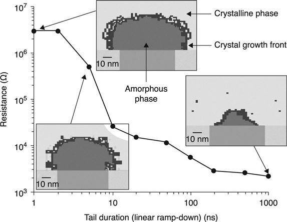
Solving simultaneously the heat diffusion equation and Laplace’s equation, to determine the temperature and voltage distributions as a function of time for a given current, can give important information about the efficiency of various cell designs, but it requires knowledge of temperature-dependent values for several material parameters such as thermal conductivity and electrical resistivity. Figure 5.10 shows a calculation of the temperature profile for various cell designs with fixed contact diameter, Φ, given by the lithographic technique, a variable length of the heater, Lh, and a variable thickness of the phase material, Lc (Russso et al. 2008). Such a calculation can determine at which Lh and Lc the current to reach the melting temperature is minimized, and helps cell designers to optimize PCM design and performance. Thermoelectric modeling also allows simulating the phase transitions from the amorphous to the crystalline and from the crystalline to the amorphous phase. Figure 5.11 shows as an example of the simulated shape of the amorphous area in a mushroom cell as a function of programming pulse shape, in particular the duration of the pulse tail assuming a linear ramp down (Nirschl et al. 2007). Short tail duration of the reset pulse leads to fast cooling and the amorphous volume is relatively large, while reset pulses with longer tails lead to partial re-crystallization at the amorphous-crystalline interface, producing smaller amorphous volumes and in consequence lower resistance of the PCM cell.

As mentioned in Section 5.3.1 and Fig. 5.5, the sub-threshold current in the amorphous phase is well described by Eq. 5.6. A refinement of the model, the distributed Pool-Frenkel model, can account for additional effects observed in PCM devices, such as the thickness dependence of resistance and activation energy (Fugazza et al. 2009). Figure 5.12(b) depicts the concept of a distribution of energy barriers in the distributed Pool-Frenkel model compared to the original assumption of one certain height of energy barrier in Fig. 5.12(a). Such a distribution of energy barriers leads to percolation effects for very thin amorphous phase change materials, thus modeling the observed reduced resistances and activation energies (Fugazza et al. 2009).

The Pool-Frenkel model can also be applied to calculate the observed resistance drift in the amorphous phase (Ielmini et al. 2007). In this model, resistance drift to higher values with time corresponds to an increase in the average distance between the traps, Δz, caused by defect annihilation and structural relaxation. This results in an increase in EC, which consequently also leads to an increase in resistance, activation energy and threshold voltage, as was observed in experiments.
For a complete modeling of the PCM operation threshold, switching also needs to be understood. Even though some aspects of the physics underlying threshold switching are still under debate, a model was developed by Ielmini and Zhang (2007) that can calculate the I-V characteristics during threshold switching in good agreement with experiments. This model is based on the assumption that at high fields above the threshold field, electrons gain substantial energy enabling them to move from low-energy states close to EF to high energy trap states close to EC, resulting in a large increase in mobility for the electrons and a large increase in current.
As mentioned in Section 5.3.1, the crystalline phase change material behaves like a p-type semiconductor. The non-linearities observed at high currents in PCM devices (Fig. 5.6) can be ascribed to thermal effects, because crystalline phase change materials, before they undergo the metal-insulator transition mentioned in Section 5.2.1, have a negative temperature coefficient of resistivity.
5.5 PCM device design and engineering
5.5.1 PCM cell concepts and designs
The mushroom cell schematically depicted in Fig. 5.8(a) was an early design (Lai and Lowrey 2001), which allowed for relative ease of fabrication, was robust in its switching properties, and enabled extensive phase change materials research. The fabrication involves the formation of the heater, which is produced by filling a small via. Such a via can have sub-lithographic dimensions if, for example, a so-called keyhole transfer process is applied that can result in vias with diameters as small as 30 nm or even less (Raoux et al. 2008b). After the via is filled by the heater material, which is often TiN, a chemical-mechanical polishing is applied to planarize the wafer followed by phase change materials deposition and patterning of the top electrode. It was realized early on that the reset current of the mushroom cell can be efficiently reduced by reducing the heater contact area (Lai 2003). Reset current in such a cell can be further reduced by using a thinner phase change material (Hwang et al. 2003).
To reduce reset currents, other cell designs were developed. The edge-contact-type cell demonstrated small reset current (200 μA), but required a relatively large footprint because of the lateral layout of the cell (Ha et al. 2003). Extensive development was performed with the so-called μTrench and self-aligned μTrench cell design, where one dimension of the phase change material-electrode contact area is given by the film thickness and can thus be very small yet well controlled (Pellizzer et al. 2004, 2006; Pirovano et al. 2005, 2007; Servalli 2009). Small reset currents of 400 μA have been achieved by this cell design.
From thermoelectric simulations, it is clear that heat loss to the electrodes can be reduced when the phase change materials are confined in a very small volume. This led to the development of the pore cell (Breitwisch et al. 2007) and the confined cell (Lee et al. 2007a). The confined cell was shown to have a reset current, which is almost half of that compared to the conventional mushroom cell, and reset currents as low as 45 μA were reported (Lee et al. 2007a). Such a cell design requires the filling of sub-lithographic vias with relatively high aspect ratios with phase change material, so novel deposition techniques such as chemical vapor deposition (CVD) or atomic layer deposition (ALD) are required, compared to the established sputter deposition technique that can be used for the fabrication of mushroom cells. Materials issues will be discussed in more detail in the next section.
Besides optimizing the shape, volume and confinement of the phase change material optimization of the bottom electrode also leads to improved device performance. Instead of using solid contacts, ring shaped contacts with reduced contact area were developed (Ahn et al. 2005; Song et al. 2006). Since the contact area is not defined by the via diameter (given by the lithographic process), but by the ring thickness determined by deposition of the contact material (which can be very well controlled), such a ring contact fabrication process shows much improved process variation. A summary of the technology characteristics of the cell designs mentioned above can be found in Table 5.3.
Table 5.3
Characteristics of various PCM cell designs
| Reference | Structure | TN (nm) | Ireset (μA) | Schematic view |
| Pellizzer et al. 2006 | Mushroom | 90 | 700 |  |
| Ha et al. 2003 | Edge | 240 | 200 |  |
| Pirovano et al. 2005, | μTrench | 180 | 450 |  |
| Pellizzer et al. 2006 | 90 | 400 | ||
| Pirovano et al. 2007 | Self-aligned μTrench | 90 | 300 |  |
| Breitwisch et al. 2007 | Pore | 180 | 250 |  |
| Lee et al. 2007 | Confined | 45 | 260 | 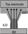 |
| Song et al. 2006 | Ring-shaped contact | 100 | 450 | 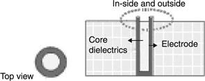 |
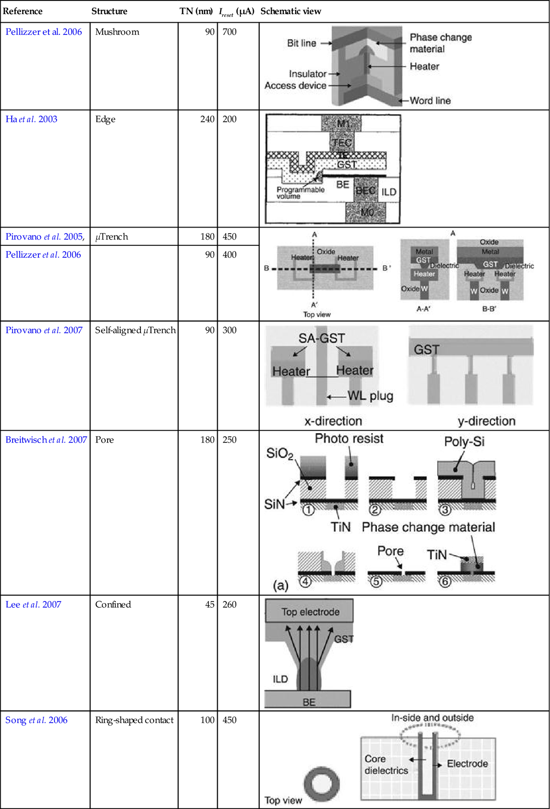
TN is the technology node, Ireset is the reset current.
Source: Adapted and reprinted with permission from Wong et al. (2010). Copyright 2010, IEEE.
5.5.2 Materials engineering for PCM
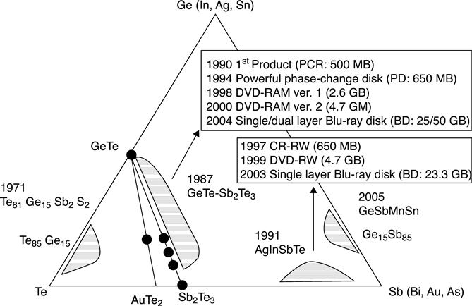
The breakthrough success of optical storage based on phase change materials came with the discovery of fast switching materials along the pseudo-binary line between GeTe and Sb2Te3, most notably Ge2Sb2Te5 (Yamada et al. 1987). Figure 5.13 summarizes the important materials used in optical storage, together with the products and years of introduction (Raoux 2009; Wuttig and Yamada 2007). Besides Ge-Sb-Te based materials, Ag- and In-doped Sb-Te alloys were also applied. This success in optical storage initiated renewed interest in PCM, and first PCM devices were fabricated that also used Ge2Sb2Te5 as the phase change material. Ge2Sb2Te5 is a phase change material that is very well suited for use in rewritable CDs operating in the infrared at 780 nm. It has strong optical contrast at 780 nm and a reasonably high crystallization temperature of around 150 °C (Friedrich et al. 2000), so that the amorphous phase is stable at the operating temperature of CDs. However, it was found that the optical contrast is much reduced at DVD and Blu-ray disc wavelengths (Fig. 5.4), and in Blu-ray discs, alloys are used that are much closer to GeTe on the pseudo-binary line between GeTe and Sb2Te3.
A similar material optimization process is taking place with respect to PCM and it can be expected that the optimum phase change material will be both application specific and also technological node specific. For example, for current PCM cell designs the threshold voltage is on the order of 1 V, while typical reading voltages are on the order of 0.2 to 0.4 V. When PCM cells are scaled to much lower physical dimensions, the threshold voltage will be reduced because it is determined by the material-specific threshold field and the dimension of the amorphous region. In such a case, the reading voltage would cause actually programming of the cell, and for these very small PCM cells materials, a much increased threshold field will be required (Krebs et al. 2009; Raoux et al. 2011a).
Table 5.1 indicates the importance of several phase change material properties. In some aspects, Ge2Sb2Te5 is a good candidate for PCM, for example it has a relatively low melting point, very low thermal conductivity, and relatively high resistance in the amorphous and the crystalline phase, but in other aspects it does not perform very well. The crystallization temperature is low for certain PCM applications such as embedded memory or automotive applications, the crystallization times are too long and cycle numbers are not sufficient for other potential PCM applications such as dynamic random access memory (DRAM) replacement. Also the large change in mass density upon phase change of about 5 to 10% (Detemple et al. 2001) can be detrimental to device performance, because it leads to void formation, which is one major failure mechanisms of PCM cells. Therefore extensive materials research has been performed to find phase change materials that are better suited for PCM.
Doping of Ge2Sb2Te5 has been widely used to modify the crystallization properties and optimize them for PCM. The term ‘doping’ in the phase change materials community is used somewhat loosely; alloying would be the more accurate term, because the ‘dopant’ concentration is typically in the several atomic % range. Often the dopant also accumulates at grain boundaries and leads to reduced crystal size of the phase change material, which can be beneficial because it increases the resistance of the crystalline phase while fine grain size at the same time reduces cell-to-cell variations. Various dopants that have been applied to study thin films of phase change materials, which include N (Dimitrov et al. 2002; Jeong et al. 2000; Privitera et al. 2004; Raoux et al. 2011a), O (Dimitrov et al. 2002; Privitera et al. 2004), SiO2 (Lee et al. 2006a; Ryu et al. 2008) and Bi (Wang et al. 2004; Watabe et al. 2004). PCM cells with doped Ge2Sb2Te5 have also been fabricated and studied where the dopants include N (Horii et al. 2003), Si (Qiao et al. 2006) and Sn (Chen et al. 2003).
Devices with other phase change materials other than Ge2Sb2Te5, such as GeTe (Bruns et al. 2009; Fantini et al. 2009; Perniola et al. 2010), C-doped GeTe (Beneventi et al. 2010), N-doped Sb2Te3 (Kim et al. 2008), SiO2-doped Ge4Sb1Te5 (Czubatyj et al. 2010), In-Ge-Te (Morikawa et al. 2007), Ge-Sb (Chen et al. 2006), GaSb (Krebs et al. 2012), Ag- and In-doped Sb2Te (Krebs et al. 2009), and even pure Sb (Krebs et al. 2009) have been fabricated and tested.
Most of the mentioned dopants improved device performance by increasing crystallization temperatures, improving data retention times, and reducing grain size and reset current. Unfortunately, dopants that increase crystallization temperatures often, at the same time, reduce crystallization speed (Shelby and Raoux 2009). Dopants can also increase the cycle numbers substantially by reducing grain size and void formation (Chen et al. 2009). Extensive ab initio calculations based on the density functional theory for the effect of Si, N and O doping in Ge2Sb2Te5 agree well with experiments and can explain the increased resistance caused by N and O doping, the increased amorphous stability of doped Ge2Sb2Te5, and the reduced crystallization speed (Cho et al. 2011).
Large efforts are devoted to find phase change materials that retain data in the amorphous phase at elevated temperatures. Embedded memory applications require data retention at 80 °C for 10 years, various automotive applications may require operation at 85 to 120 °C, and for pre-coded chips that need to pass the solder-bonding process data, need to be retained at temperatures even as high as 250 to 260 °C for several seconds. By modifying Ge-Sb-Te materials, not along the GeTe-Sb2Te3 line but along the isoelectronic line for alloys of the composition Ge:Sb:Te = 1:x:1 with variable x between 1 and 6, materials were found that showed very promising high temperature data retention behavior (Cheng et al. 2010b; Raoux et al. 2011b). Alloys with small x were found to have very high crystallization temperatures, as high as 250 °C compared to 150 °C for Ge 2Sb2Te5.
Further improvement regarding high temperature data retention was achieved by adding additional Ge to the Ge:Sb:Te = 2:1:2 alloy (Cheng et al. 2011b) and chips were fabricated that showed high cycle numbers and excellent high temperature data retention. Even though adding Ge to a Ge-Sb-Te alloy increases the crystallization temperature, and in return improves data retention at high temperatures, it has a negative effect on the resistance drift as it increases the drift exponent (Li et al. 2011). This can be attributed to a larger number of gap states in Ge-rich alloys, as calculated by ab initio molecular dynamics calculations.
Doping with nitrogen increased the crystallization temperature of the N-Ge-Sb-Te alloys even further, by up to around 420 °C (Cheng et al. 2012). These alloys demonstrated excellent data retention at high temperatures at the chip level. Predicted data retention for ten years was reported at 85 °C for N-doped Ge2Sb2Te5 (Kim et al. 2010) and 100 °C for O-doped Ge2Sb2Te5 (Oh et al. 2006), while these N-Ge-Sb-Te alloys result in predicted data retention for ten years at 120 °C. This makes them very attractive for high temperature applications.
Another important material optimization factor is the set time (crystallization time). For possible DRAM replacement application, PCM cells need to switch on to the nanosecond timescale. By selecting the phase change material, crystallization times can vary by orders of magnitude (Raoux et al. 2008a). Materials that show very fast switching in laser testing experiments include the Ge:Sb:Te = 1 × 1 alloys with large x, such as Ge:Sb:Te = 1:6:1 (Cheng et al. 2010b). Fortunately, the scaling behavior for PCM cells is in favor of fast switching and smaller PCM cells have shorter crystallization times, which can be on the 1 ns timescale (Bruns et al. 2009; Loke et al. 2011; Wang et al. 2009). Ultrafast switching in 500 ps for both set and reset operation was recently demonstrated using a special programming scheme (Loke et al. 2012).
Regarding materials optimization, we also need to consider deposition methods. Sputter deposition has been the traditional method because it is a reliable and reproducible, very well established process that can be scaled up to large wafer sizes. However, it limits the cell design to phase change fabrication processes that do not require the filling of small vias, because sputter deposition is neither very directional nor conformal. Therefore, other deposition methods have been explored. Among those, chemical vapor deposition (CVD) and atomic layer deposition (ALD) are the most developed. Both methods show very good via filling capabilities. CVD was shown to fill vias of high aspect ratio and with constant material composition through the depth of the via (Lee et al. 2007a). Ultrascaled devices with the phase change material dimension being only 7.5 nm wide were perfectly filled with phase change material using CVD (Im et al. 2008; Oh et al. 2009). Figure 5.14 shows transmission electron microscope (TEM) images of this so-called dash-type confined cell structure.

ALD is an ideal deposition method for device fabrication, because it shows excellent conformality, uniformity and precise thickness control. However, ALD of phase change materials was initially problematic, because it required the development of precursor materials for Ge, Sb and Te. A breakthrough for ALD of phase change materials occurred when it was found that alkyl silyl compounds of Te and Se react efficiently with Ge and Sb chlorides (Pore et al. 2009). Since then, ALD of phase change materials has been rapidly developed and a large variety of materials have been deposited (Fig. 5.15) and characterized (Pore et al. 2011). Excellent conformality and via filling capabilities were also demonstrated (Ritala et al. 2009, 2012).

5.5.3 Advanced PCM prototype devices and scaling
Since the introduction of PCM technology, one of the most important questions has been what the scaling limits are for this technology. In Section 5.3.2, the scaling limits of the phase change materials were discussed. Here advanced PCM devices and ultrascaled prototypes will be described. One of the first attempts to test the scaling limits was the fabrication of very small line devices with a width of about 50 nm (Lankhorst et al. 2005). These devices could be switched repeatedly and showed all the properties of larger PCM cells. The limits of PCM cell size were further pushed to smaller dimensions by Chen et al. (2006) with a similar cell design, the bridge cell. Ge-Sb, with the eutectic composition of 15:85 atm.%, was the phase change material used and the cross-sectional dimension of the smallest bridge were 20 nm wide, fabricated by electron beam lithography, and 3 nm in height, given by the film thickness. Electrical testing proved that even the smallest devices were fully functional. These devices could be switched in times as short at 40 ns with a small reset current of 90 μA.
Another approach to fabricate ultrascaled PCM cells uses phase change nanowires grown by the vapor-liquid-solid (VLS) technique using Au nanoparticles as the catalyst (Sun et al. 2007). PCM devices were fabricated by transferring the as-deposited nanowires onto SiO2 substrates and contacting the phase change nanowires with Pt pads deposited by a focused ion beam (Jung et al. 2006; Lee et al. 2006a, 2007b). The nanowire material included GeTe and Ge2Sb2Te5 phase change materials. These PCM devices could also repeatedly be switched for cycle numbers of up to 106.
As mentioned in the previous section, CVD has allowed the fabrication of very small dash-type confined cells with one cell dimension given by a film thickness as small as 7.5 nm (Im et al. 2008; Oh et al. 2009) (Fig. 5.14). With these devices, even multiple-level storage could be demonstrated by having up to three parallel confined cells connected to the same top and bottom electrode (Oh et al. 2009).
Some of the very smallest PCM devices were fabricated using carbon nanotubes as the electrodes (Xiong et al. 2011, 2012, 2013). The most advanced devices use a single-wall or small (diameter ~ 5 nm) multi-wall carbon nanotube covered with photoresist. To fabricate PCM cells, a current is required to flow through the carbon nanotube, which is contacted by Pd pads, leading to evaporation of the photoresist caused by Joule heating and thus forming a narrow self-aligned trench around the nanotube. Subsequently, a small gap (20–150 nm) is created in the nanotube by applying a high electrical pulse that causes electrical breakdown. Phase change material is then sputtered and the photoresist lifted off. The device dimensions are determined by the diameter of the nanotube and the size of the gap in the nanotube. Even these ultrascaled devices show typical PCM switching behavior and ultra-low reset currents of approximately 1.9 μA. All the prototype device research indicates a very favorable scaling behavior for PCM technology.
5.5.4 PCM process integration
The ultimate goal of PCM technology development is the fabrication of highly functional, low cost, reliable, reproducible, large (megabits to gigabits) memory chips, which are compatible with existing CMOS (Complementary Metal-Oxide-Semiconductor) fabrication processes. Fabrication cost is determined by many factors, but chips which require fewer process steps are favorable because the additional process steps increase costs and also the probability of defects. In addition, smaller chips with higher storage density also keep costs low, because the number of chips per wafer is increased.
The requirements for memory devices depend on the application and vary in programming and read speed, the number of cycles the memory needs to be written (endurance), the data retention, the memory size, and additional external factors such as the robustness with respect to extreme temperatures, shock or radiation. A memory design needs to take all these factors into consideration and optimize the array design for a specific application.
Figure 5.9 demonstrates the basic layout of a PCM cell array. The memory cell is essentially a programmable resistor connected to the access device, which provides the electrical pulses for programming and reading, and isolates the memory cell from neighboring cells so they are not disturbed when the memory cell is programmed or read. As mentioned before, the access device can be a metal-oxide-semiconductor field-effect transistor (MOSFETs) (Lai 2003), a bipolar junction transistor (BJTs) (Pellizzer et al. 2006) or a diode (Oh et al. 2006). The access device needs to deliver enough current for the reset operation, and this is one of the major requirements that dictate many aspects of access device selection. There are trade-offs between the options where BJTs and diodes can typically deliver larger currents, but MOSFETs provide better isolation. The different access devices have also very different footprints, with diodes having the smallest 5.8F2 have been demonstrated where F is the minimum lithograph feature size of the given technology node (Oh et al. 2006)), while MOSFET access devices typically lead to much larger cell size of MOSFET plus PCM occupying 25F2.
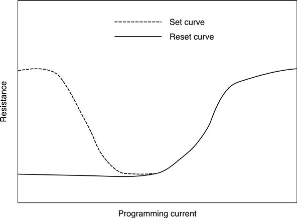
Different PCM cell designs have been already described in Section 5.5.1. The PCM cells and access devices need to be designed together, so that optimum memory array performance is guaranteed. There are multiple ways to characterize a memory array. The IV-curve of a PCM cell is shown in Fig. 5.6, and from such a measurement the threshold voltage can be detected. The programming curve of a PCM cell is shown schematically in Fig. 5.16. If the cell is initially in the set state (low resistance state) and electrical pulses of increasing programming current are applied, the phase change material starts to melt and quench during cooling in the amorphous state and leading to increased resistance. Eventually all of the material that switches phase has been melt-quenched by the current pulse and the resistance saturates at the full reset value. If the cell is initially in the reset state (high resistance), increasing the applied current pulses starts to heat the amorphous material above the crystallization temperature, the material crystallizes and the resistance drops until it reaches the fully set state of low resistance. For higher current pulses, the cell is reset again. Cell arrays show a distribution of the set and reset state resistances due to process variation, cell-to-cell variations and the programming conditions. Figure 5.17 shows resistance distributions for varying programming pulse widths (Kang et al. 2007). A wide window between the set and rest resistance distribution is desirable for reliable programming and good data retention.

The programming characteristic of PCM lends itself to the potential storage of multiple levels per cell. Figures 5.11 and 5.16 show that PCM cells can be switched to intermediate resistance states. This effect was utilized to program up to 16 distinct and separated resistance levels in a PCM 10 × 10 cell array test structure using a write-verify programming scheme (Nirschl et al. 2007). Such a utilization of PCM cells is very attractive, because it can increase storage density substantially. However, it is complicated by the resistance drift mentioned in Section 5.3.1. However, special novel measurement metrics compared to the resistance metric can be applied, which are robust to resistance drift. In addition, new modulation coding techniques have been developed that allow multilevel storage in PCM and data retention over extended periods of time (Pozidis et al. 2011).
5.6 Conclusion and future trends
The ability to set a PCM cell in various resistance states does not only enable multilevel memory storage, butt also opens the opportunity of phase change devices to other applications such as logic and neuromorphic computing. It was shown that computation can be performed using phase change thin films and a laser tester, or using PCM cells by applying multiple small laser or electrical pulses. Each pulse alone was not enough to switch the film or cell, respectively, but the accumulation of pulses switched the film or cell at a given threshold number of pulses, which depends on the conditions of the small pulses (Wright et al. 2011, 2012). Operations such as addition, subtraction, multiplication and division were demonstrated, as well as logic operations such as AND and OR. Other novel application include the use of phase change cells as synapses in neuromorphic computing (Jackson et al. 2013; Jo et al. 2010; Kuzum et al. 2011; Rajendran et al. 2013). Change in synaptic strength is assumed to be the learning mechanism in biological synapses. Synaptic plasticity allows that the connection strength between neurons is modified, depending on the activities in the presynaptic and postsynaptic neurons (spike-timing dependent plasticity (Bi and Poo 1998)). Neuromorphic or brain-inspired computing requires hardware components that function like brain components, and a PCM cell is a potential candidate for fulfilling synaptic functions. PCM cell switching, that mimics spike-timing dependent plasticity, has been indeed implemented in PCM cells using a special programming scheme (Jackson et al. 2013; Kuzum et al. 2011). Scalable CMOS integration schemes for implementing neuromorphic computing have also been proposed(Rajendran et al. 2013).
Intense research efforts over the last decades have led to a much better understanding of the phase change processes in phase change material. This enables the design of new and improved phase change materials, not only by trial and error, but also by predicting properties of phase change materials based on simulations. The technology has been developed in parallel, PCM chips with very attractive functionality are now fabricated and first PCM products are on the market. Because of the excellent scaling capabilities of PCM, it can be expected that it will play an increasing role for future technology nodes. Besides memory applications, phase change materials may also find new applications in fields such as logic and neuromorphic computing.