
9.8 Compensation devices at fundamental and harmonic frequencies
One of the main responsibilities of a utility system is to supply electric power in the form of sinusoidal voltages and currents with appropriate magnitudes and frequency for the customers at the points of common coupling (PCC). Design and analysis of system equipment and user apparatus are based on sinusoidal current and voltage waveforms with nominal or rated magnitudes and frequency. Although the generated voltages of synchronous machines in power plants are nearly sinusoidal, some undesired and/or unpredictable conditions – such as lightning and short-circuit faults – and nonlinear loads cause steady-state and/or transient voltage and current disturbances. For example, electric arc furnaces cause voltage fluctuations, power electronic converters generate current harmonics and distort voltage waveforms, and short-circuit faults result in voltage sags and swells. On the other hand, most customer loads such as computers, microcontrollers, programmable logic controllers (PLCs), and hospital equipment are sensitive and unprotected to power quality disturbances and their proper operation depends on the quality of the voltage that is delivered to them.
To optimize the performance and stability of power systems and to overcome power quality problems, many techniques and devices have been proposed and implemented. Conventional devices used for voltage regulation, power factor correction, and power quality improvement include shunt or series power capacitors, phase shifters, and passive or active filters (Sections 9.1 to 9.7). Advanced technical solutions are flexible AC transmission system (FACTS) devices [18,19] to improve voltage regulation, as well as steady-state and instantaneous active and reactive power control at fundamental frequency. Other approaches are based on custom power devices [20,21] that offer a variety of options including series and shunt active (P) and reactive (Q) power compensation to improve power quality, voltage regulation, as well as steady-state and dynamic performances at fundamental and harmonic frequencies.
The concept of hybrid active filtering with shunt and series branches was introduced by Akagi and colleagues [22–24]. The most complete configuration of hybrid filters is the unified power quality conditioner (UPQC), which is also known as the universal active filter [25–30]. UPQC is a multifunction power conditioner that can be used to compensate various voltage disturbances of the power supply, to correct voltage fluctuation, and to prevent the harmonic load current from entering the power system. It is a custom power device designed to mitigate the disturbances that affect the performance of sensitive and/or critical loads. UPQC has shunt and series compensation capabilities for (voltage and current) harmonics, reactive power, voltage disturbances (including sags, swells, flicker, etc.), and power-flow control. Normally, a UPQC consists of two voltage-source converters with a common DC link designed in single-phase, three-phase three-wire, or three-phase four-wire configurations. One converter is connected in series through a transformer between the source and the critical load at the PCC and operates as a voltage-source inverter (VSI). The other converter is connected in shunt at the PCC through a transformer and operates as a current-source inverter (CSI). The active series converter compensates for voltage supply disturbances (e.g., including harmonics, imbalances, negative and zero-sequence components, sags, swells, and flickers), performs harmonic isolation, and damps harmonic oscillations. The active shunt converter compensates for load current waveform distortions (e.g., caused by harmonics, imbalances, and neutral current) and reactive power, and performs the DC link voltage regulation.
UPQC is specifically designed to protect the critical load at the point of installation connected to distorted distribution systems by correcting any of the following shortcomings:
• harmonic distortions (of source voltage and load current) at the utility–consumer PCC,
• voltage disturbances (sags, swells, flickers, imbalances, and instability),
• voltage regulation,
• reactive power flow at fundamental and harmonic frequencies,
• neutral and negative-sequence currents, and
• harmonic isolation (e.g., between a subtransmission and a distribution system).
Therefore, UPQC has the capability of improving power quality at the point of installation of power distribution systems. This includes compensation of voltage-based disturbances across the sensitive load (such as voltage harmonics, voltage imbalances, voltage flickers, sags, and swells) and current-based distortions of the system (such as current harmonics, reactive power, and neutral current). However, UPQC is not capable of improving the power quality of the entire system.
The main compensation devices for power quality improvement are introduced, and in Section 9.9 the UQPC structure and operation are discussed. Section 9.10 discusses the control system of the UPQC. Sections 9.11 and 9.12 provide detailed analyses and discussions of two main approaches for implementing UPQC control systems including the Park (dq0) transformation and the instantaneous real and reactive power approach. Section 9.13 explores UPQC performance through six application examples.
Over the past several decades the transmission and distribution of electric power has become extremely complicated and subject to very tight operational and power quality specifications: the loads are increasing, power transfer grows, and the power system becomes increasingly more difficult to operate and less secure with respect to major disturbances and outages. The full potential of transmission interconnections may not be utilized due to:
• large power flow with inadequate control pooling,
• excessive reactive power in various part of the power system, and
• large dynamic power swings between different parts of the system.
The main problems with interconnected transmission lines are:
• at no-load or light-load condition the voltage increases at receiving ends resulting in reduced stability,
• at loaded conditions the voltage drop increases resulting in the decrease of transmittable power,
• voltage collapse and voltage instability,
• power and power angle variation due to small disturbances, and
• transient instability due to sudden and severe power variations or oscillations.
As the length of a line increases these problems become more pronounced. The ultimate solution is the instantaneous control of the bus voltage (V), the active power (P), the reactive power (Q), and the total harmonic voltage distortion (THDv).
9.8.1 Conventional Compensation Devices
The conventional approaches for voltage regulation and power compensation at fundamental frequency are relatively simple and inexpensive. They include:
• shunt compensators (capacitors, reactors),
• series compensators (series capacitors), and
• phase shifters.
These devices are mechanically controlled at low speed and there are wear-and-tear problems resulting in greater operating margins and redundancies. If conventional compensation devices are employed, the system is not fully controlled and optimized from a dynamic and steady-state point of view.
Conventional devices used for power quality improvement are passive and active power filters, as discussed in Sections 9.1 to 9.7. Passive filters are simple and inexpensive. However, they have fixed (tuned) frequencies and will not perform properly under changing system configurations and/or variable (nonlinear) load conditions. Active filters eliminate harmonics at the point of installation without considering the power quality status of the entire system. In addition, they do not solve the stability problem, and are not generally capable of optimizing the performance (e.g., voltage regulation, reactive power compensation) of power systems.
9.8.2 Flexible AC Transmission Systems (FACTS)
In order to meet stringent specifications and the established contractual obligations set out in supply agreements, various technologies have been used. Among the newly developed technical solutions are FACTS, which were introduced by GyuGyi [18,19]. They offer a variety of options including series and shunt compensation of power at fundamental frequency to achieve instantaneous and individual or simultaneous control of V, P, and Q. FACTS devices are designed to improve the reliability and the quality of power transmission. However, they do not consider the quality of power that is delivered to customers. This section briefly introduces different types of FACTS controllers [19].
Shunt FACTS Controllers
Three types of shunt FACTS controllers are employed to inject compensation current into the system. An injected current in phase quadrature with the phase voltage results in Q control; other phase relations provide simultaneous control of P and Q.
• Variable impedance shunt FACTS controllers are also called static VAr generators (SVGs) or static VAr compensators (SVCs). They are thyristor-controlled reactors and/or thyristor-switched capacitors and consist of the following types:
• Thyristor-controlled reactors (TCRs) and thyristor-switched reactors (TSRs),
• Thyristor-switched capacitor (TSC),
• Fixed capacitor, thyristor-controlled reactor (FC-TCR), and
• Thyristor-switched capacitor, thyristor-controlled reactor (TSC-TCR).
• Switching converter SVG shunt FACTS controllers are switching converter based controllable synchronous voltage sources and consist of the following type:
• Static synchronous compensator (STATCOM).
• Hybrid SVG and switching converter shunt FACTS controllers are switching type SVGs with fixed (or controllable) capacitors and/or reactors. They include:
• STATCOM with fixed capacitors (STATCOM & FC),
• STATCOM with fixed reactors (STATCOM & FR), and
• STATCOM with TSC and TCR units (STATCOM & TSC-TCR).
Series FACTS Controllers
There are two basic types of series compensation:
• Variable impedance series FACTS controllers use thyristor-switches to provide series variable reactive impedances. They include:
• Gate turn-off (GTO) thyristor-controlled series capacitor (GCSC),
• Thyristor-switched series capacitor (TSSC), and
• Thyristor-controlled series capacitor (TCSC).
• Switching converter series FACTS controllers use switching converters to provide variable series voltage sources. They include
Combined Shunt–Series FACTS Controllers
These controllers may consist of a number of shunt, a number of series, or a combination of shunt and series FACTS devices. Three popular combined shunt–series FACTS controllers are
• Unified power flow controller (UPFC) has one converter in series and the other in shunt with the transmission line,
• Interline power flow controller (IPFC) has both converters in series with usually a different line, and
• Back-to-back STATCOM has both converters in shunt, each connected to a different power system.
FACTS Controllers with Storage
Any of the converter-based FACTS devices can generally accommodate storage such as capacitors, batteries, and superconducting coils. These controllers are more effective for controlling system dynamics due to their ability to dynamically provide/extract real power P to/from a system.
Development of FACTS Controllers
The first generation of FACTS (e.g., SVC, TSSC, TCSC, thyristor controlled phase shifters, etc) use thyristor controlled switches as control devices. The second generation (e.g., STATCOM, SSSC, UPFC, IPFC, etc) are converter-based devices and use switching static converters as fast controllable voltage and current sources.
The application of FACTS devices is increasing as their advantages become more evident to power system engineers and researchers. FACTS controllers are primarily designed to operate at fundamental power frequency under sinusoidal conditions and do not necessarily improve the quality of electric power. In fact, most FACTS controllers use switching devices that inject current and voltage harmonics into power systems. Corrective approaches (e.g., sinusoidal PWM techniques) have been proposed to minimize their limitations.
9.8.3 Custom Power Devices
The introduction of power electronic loads has raised much concern about power quality problems caused by harmonics, distortions, interruptions, and surges. Equipment such as large industrial drives (e.g., cycloconverters) generate significantly high voltage and current (inter-, sub-) harmonics and create extensive voltage fluctuation. This is more evident in power systems that make use of long transmission lines with limited reactive capacities.
The application of harmonic filters and SVCs to radial transmission systems can offer partial solution to high THD levels and voltage fluctuations. Yet, the lack of dynamic capabilities of these devices limits them to bulk correction. In addition, they might be effective in one application but fail to correct other power quality issues.
The concept of custom power was introduced by Hingorani [20] as the solution to V, P, and Q compensation and power quality problems at the expense of high cost and network complexity. As FACTS controllers improve the reliability and quality of power transmission – by simultaneously enhancing both power transfer capacity and stability – custom power devices enhance the quality and reliability of power delivered to the customer. With a custom power device, a customer (e.g., a sensitive load) will be able to receive a prespecified quality of electric power with a combination of specifications including but not limited to:
• magnitude and duration of over- and under-voltages with specified limits,
• low harmonic distortion in the supply, load voltages, and currents,
• small phase imbalance,
• low flicker in the supply voltage,
• control of power interruptions, and
• control of supply voltage frequency within specified limits.
Custom power devices are classified based on their power electronic controllers, which can be either of the network-reconfiguration type or of the compensation type. The network-reconfiguration devices –also called switchgear – include the solid-state and/or static versions of current limiting, current breaking, and current transferring components. The compensation-type custom power devices either compensate a load (e.g., correct its power factor, imbalance) or improve the quality of the supply voltage (e.g., eliminate its harmonics). They are either connected in shunt or in series or a combination of both. Custom power devices are classified as follows [21]:
• Network-reconfiguration custom power devices include:
• Solid-state current limiter (SSCL),
• Solid-state breaker (SSB), and
• Solid-state transfer switch (SSTS).
• Compensation-custom power devices include:
• Distribution STATCOM (DSTATCOM),
• Dynamic voltage restorer/regulator (DVR), and
• UPQC
Custom power devices are designed to improve the quality of power at their point of installation of the power distribution systems. They are not primarily designed to improve the power quality of the entire system.
9.8.4 Active Power Line Conditioner (APLC)
The APLC is a converter-based compensation device designed to improve the power quality of the entire distribution system by injecting corrective harmonic currents at selected (sensitive) buses. It is usually necessary to use more than one APLC unit to improve the power quality of the entire distribution system. Therefore, APLC units can be considered as a group of shunt active filters; their placement, sizing, and compensation levels (e.g., orders, magnitudes, and phases of injected current harmonics) are optimally designed to improve the power quality of the entire distribution system. The number of required APLC units depends on the severity of distortion, the nature of the distribution system, and types of nonlinear loads, as well as the required quality of electric power (e.g., as specified by IEEE-519). At present, the design of APLCs does not consider transient distortions and stability issues.
9.8.5 Remarks Regarding Compensation Devices
In the absence of saturation and nonlinearity, power system voltage and current waveforms are sinusoidal and FACTS controllers are employed to solve the associated steady-state, transient, and stability problems. Custom power devices are designed to improve the steady-state and transient problems of distorted distribution systems at the point of installation. Power filters and APLCs mitigate power quality problems at a given location and throughout the power system, respectively. However, at present, none of them are designed to simultaneously consider stability and power quality issues. This is highly related to the fact that in conventional centralized power systems, power quality problems are limited to the low- and medium-voltage distribution systems, whereas stability issues are mainly occurring in high-voltage transmission systems. With the introduction of distributed generation (DG) and the fast growing rate of renewable energy sources in today’s power system, there will be an overlap between stability and power quality issues. More attention and further research is required to analyze and examine stability issues in decentralized distorted networks, as well as isolated and DG power systems.
9.9 Unified power quality conditioner (UPQC)
Unified power quality conditioners are viable compensation devices that are used to ensure that delivered power meets all required standards and specifications at the point of installation. The ideal UPQC can be represented as the combination of a voltage-source converter (injecting series voltage vc), a current-source converter (injecting shunt current ic), and a common DC link (connected to a DC capacitor). There are two possible ways of connecting the unit to the terminal voltage (vt) at PCC:
• Right-shunt UPQC (Fig. 9.30a), where the shunt compensator (ic) is placed at the right side of the series compensator (vc).

• Left-shunt UPQC (Fig. 9.30b), where the shunt compensator (ic) is placed at the left side of vc.
These two structures have similar features; however, the overall characteristics of the right-shunt UPQC are superior (e.g., operation at zero power injection/absorption mode, achieving unity power factor at load terminals, and full reactive power compensation). In this chapter, a right-shunt UPQC configuration is assumed and analyzed. References [21] and [26] present detailed analysis of the left-shunt structure.
9.9.1 UPQC Structure
The detailed structure of the right-shunt UPQC is shown in Fig. 9.31. Assuming a three-phase, four-wire configuration with an unbalanced and distorted system voltage (vs) and nonsinusoidal load current (iL), the UPQC shall perform the following functions:

• convert the feeder (system) current is to balanced sinusoids through the shunt compensator,
• convert the load voltage vL to balanced sinusoids through the series compensator,
• ensure zero real power injection (and/or absorption) by the compensators, and
• supply reactive power to the load (Q compensation).
UPQC employs two converters that are connected to a common DC link with an energy storage capacitor. The main components of a UPQC are series and shunt power converters, DC capacitors, low-pass and high-pass passive filters, and series and shunt transformers:
• Series converter is a voltage-source converter connected in series with the AC line and acts as a voltage source to mitigate voltage distortions. It eliminates supply voltage flickers or imbalance from the load terminal voltage and forces the shunt branch to absorb current harmonics generated by the nonlinear load. Control of the series converter output voltage is usually performed using pulse-width modulation (PWM). The gate pulses are generated by the comparison of a fundamental voltage reference signal with a high-frequency triangular waveform.
• Shunt converter is a voltage-source converter connected in shunt with the same AC line and acts as a current source to cancel current distortions, to compensate reactive current of the load, and to improve the power factor. It also performs the DC-link voltage regulation, resulting in a significant reduction of the DC capacitor rating. The output current of the shunt converter is adjusted (e.g., using a dynamic hysteresis band) by controlling the status of semiconductor switches such that output current follows the reference signal and remains in a predetermined hysteresis band.
• Midpoint-to-ground DC capacitor bank is divided into two groups, which are connected in series. The neutrals of the secondary transformers are directly connected to the DC link midpoint. As the connection of both three-phase transformers is Y/Y0, the zero-sequence voltage appears in the primary winding of the series-connected transformer in order to compensate for the zero-sequence voltage of the supply system. No zero-sequence current flows in the primary side of both transformers. It ensures the system current to be balanced even when the voltage disturbance occurs.
• Low-pass filter is used to attenuate high-frequency components at the output of the series converter that are generated by high-frequency switching.
• High-pass filter is installed at the output of shunt converter to absorb current switching ripples.
• Series and shunt transformers are implemented to inject the compensation voltages and currents, and for the purpose of electrical isolation of UPQC converters.
The UPQC is capable of steady-state and dynamic series and/or shunt active and reactive power compensations at fundamental and harmonic frequencies. However, the UPQC is only concerned about the quality of the load voltage and the line current at the point of its installation, and it does not improve the power quality of the entire system.
9.9.2 Operation of the UPQC
The shunt converter forces the feeder (system) current to become a balanced (harmonic-free) sinusoidal waveform, while the series converter ensures a balanced, sinusoidal, and regulated load voltage.
9.9.2.1 Operation of the UPQC with Unbalanced and Distorted System Voltage and Load Current
In most cases the three-phase system voltages and load currents are unbalanced and contain higher order frequency components (harmonics), and a UPQC unit is used to compensate for both types of distortions. The UPQC takes the following two steps to compensate for the imbalance and the distortion of system voltage and line current [21].
Step 1: Obtaining Balanced Voltage at Load Terminals
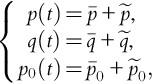
The imbalance or distortion of a three-phase system may consist of positive, negative, and zero-sequence fundamental and harmonic components. The system (utility) voltage at point S (Fig. 9.31) can be expressed as
where subscripts +, –, and 0 refer to the positive-, negative-, and zero-sequence fundamental components, respectively; vs +(t) = Vs + sin(ωt + ϕ+), vs–(t) = Vs– sin(ωt + ϕ–), and vs0(t) = Vs0 sin(ωt + ϕ0) are positive-, negative-, and zero-sequence fundamental frequency components of the system voltage; ∑ Vsh(t) = ∑ Vsh sin (hωt + ϕh) represents the harmonics in the voltage, h is harmonic order; and ϕ+, ϕ–, ϕ0, and ϕh are the corresponding voltage phase angles.
Usually, the voltage at the load at PCC is expected to be sinusoidal with a fixed amplitude VL:
Hence the series converter will need to compensate for the following components of voltage:

The control system should automatically control the series converter so that its generated voltage at its output terminals is vc(t) (in Fig. 9.31) and matched with Eq. 9-25.
Step 2: Obtaining Balanced System Current Through the Feeder
The distorted nonlinear load current (Fig. 9.31) can be expressed as
where iL+(t) = IL + sin(ωt + δ+), iL–(t) = IL– sin(ωt + δ–), and iL0(t) = IL0 sin(ωt + δ0) are the fundamental frequency positive-, negative- and zero-sequence components of the load current and ΣiLh(t) = ΣILhsin(hωt + δh) represents the harmonics of the load current. δ+, δ–, δ0, and δh are the corresponding current phase angles.
The shunt converter is supposed to provide compensation of the load harmonic currents to reduce voltage distortion. It should act as a controlled current source and its output current must consist of harmonic, negative-, and zero-sequence currents to cancel the load current distortions. It is usually desired to have a certain phase angle (displacement power factor angle), θL, between the positive sequences of voltage and current at the load terminals:
Substituting Eq. 9-27 into Eq. 9-26 and simplifying yields

It is clear that the output current of the shunt converter should be controlled and must assume a wave shape as specified by the 2nd, 3rd, 4th, and 5th terms of Eq. 9-28. That is,
This will ensure that the system (feeder) current has a sinusoidal waveform:
Equations 9-25 and 9-29 demonstrate the principles of an ideal UPQC. If these equations are dynamically implemented by the UPQC controller, terminal load voltage and system current will be sinusoidal. In addition, system voltage and current will be in phase if θL = 0 (e.g., unity power factor), and neither positive nor negative reactive power will be supplied by the source.
9.9.2.2 Operation of UPQC with Unbalanced System Voltages and Load Currents
Assuming that the system voltages and load currents are unbalanced but not distorted (harmonic-free), one can generate UPQC equations as shown below. The UPQC takes the following four steps to compensate the imbalance of the system voltages and line currents [21].
Step 1: Obtaining Balanced Voltages at Load Terminals
From the structure of the ideal right-hand UPQC (Fig. 9.31) follows
To obtain balanced voltages at the load terminals, vc(t) must cancel the imbalance of the system voltages; therefore,
which implies that VL is of positive sequence. Note that the positive-sequence magnitude of the load voltage (VL) should be set to the desired regulated voltage, whereas its phase angle depends on the load displacement power factor.
One defines an injected positive-sequence voltage (|Vc+|) such that the series compensator does not require any positive-sequence (real) power. Because is flows through the series compensator, vc + must have a phase difference of 90° with is +. This implies
where (a + jb) is the unit vector that is perpendicular to Is+. Assuming VL + = VL∠0°, Eq. 9-33 results in the following second-order equation:
If the desired regulated voltage level VL is achievable, this quadratic equation will have two real solutions for |Vc+|. The minimum solution should be selected because it will result in less cost (e.g., smaller rating) of the UPQC.
Step 2: Obtaining Balanced System Currents Through the Feeder
From the structure of the ideal right-hand UPQC (Fig. 9.31) one gets
To obtain balanced system currents, the injected current ic(t) must become zero and one gets for the sequence components of the load current
This will ensure that a positive-sequence current (equal to the positive-sequence load current) only is passing through the system.
Step 3: Ensuring Zero Real Power Injection/Absorption by the Compensators
Equations 9-31 to 9-36 guarantee that imbalances in both the system voltages and the load currents are cancelled by the UPQC. Moreover,
• The series compensator (converter) will consume zero average (real) power because its voltage and current are in quadrature (e.g., ![]() is in quadrature with
is in quadrature with ![]() ).
).
• The shunt compensator (converter) will also inject zero average (real) power since its positive-sequence injected current is zero (Ic + = 0) and the load voltage is of positive sequence only.
Therefore, the UPQC does neither inject nor absorb real power.
Step 4: Reactive Power Injection by the Compensators
The UPQC can supply part of the load reactive power through its shunt compensator (converter). To do this Eq. 9-36 has to be modified while keeping in mind that the zero and negative-sequence components of the load current must also be canceled by the shunt converter. The new conditions for the injected shunt currents are now
We can divide the average component of the load reactive power between the shunt converter, the series converter, and the system. Due to the fact that the average values of the active and the reactive powers of the shunt converter depend only on the positive-sequence current and its real power consumption (or absorption) must be zero, one gets

where θ is the angle between VL + and Ic +, scalar β indicates how much reactive power must be supplied by the shunt converter, and QL-avg is the average of the load reactive power.
For inductive loads (e.g., negative QL-avg), compensator (converter) current Ic + must lag VL by 90° (to satisfy Eq. 9-38a) and one can write

The cancellation of the supply and load current imbalances using an UPQC is addressed in [21, pp. 383–385] and the reactive power compensation with a UPQC is discussed in [21, pp. 386–388].
9.10 The UPQC control system
It is possible to distinguish between disturbances related to the quality of the system (supply) voltage and those related to the quality of the load current. The UPQC corrects both problems at the point of installation (e.g., at the terminals of a sensitive or critical load). It combines a shunt active filter together with a series active filter in a back-to-back configuration to simultaneously improve the power quality of the supply current through the power system and the load voltage at PCC. The main functions of the UPQC are summarized in Table 9.1.
Table 9.1
Main Functions of UPQC Controller

The main components of a UPQC are the series and shunt converters representing active filters, high and low-pass passive filters, DC capacitors, and series and shunt transformers, as shown in Fig. 9.31. The shunt converter is a STATCOM that injects nonsinusoidal corrective current to improve the power quality, regulate load voltage, and control the load power factor. It also compensates for the load reactive power demand, corrects supply current harmonics, and regulates the DC-link voltage. The series converter represents a dynamic voltage regulator (DVR) that introduces corrective harmonic voltages to ensure sinusoidal supply current and constant voltage conditions under steady-state and transient operating conditions (e.g., during voltage sags and swells).
The power electronic converters are frequently voltage-source inverters (VSIs) with semiconductor switches. The output current of the shunt converter is adjusted using an appropriate control scheme (e.g., dynamic hysteresis band). The states of semiconductor switches are controlled so that the output current tracks the reference signal and remains in a predetermined hysteresis band. The installed passive high-pass filter – at the output of shunt converter – absorbs the current switching ripples.
Control of the series converter output voltage is performed using PWM techniques. The gate pulses are generated by the comparison of a fundamental voltage reference signal with a high-frequency triangular waveform. The low-pass filter attenuates high-frequency components at the output of the series converter, generated by high-frequency switching.
For the compensation of the zero-sequence components, the split-capacitor scheme is usually used on the DC side of converters and the capacitor’s midpoint is connected to the neutral. In order to inject the generated voltages and currents, and for the purpose of electrical isolation of UPQC converters, series and shunt transformers may also be included in the UPQC configuration.
9.10.1 Pattern of Reference Signals
Provided unbalanced and distorted source voltages and nonlinear load currents exist, then – based on Eqs. 9-23 to 9-39 – the output voltage of the series converter (vc(t), Fig. 9.31) and the output current of shunt converter (ic(t), Fig. 9.31) must obey the following equations:

so that the current drawn from the source and the voltage appearing across the load will be sinusoidal.
Generation, tracking, and observation of these reference signals are performed by the UPQC control system. There are two main classes of UPQC control: the first one is based on the Park transformation [32], and the second one on the instantaneous real and imaginary power theory [26,30,31]. These will be introduced in the following sections. There are other control techniques for active and hybrid (e.g., UPQC) filters as discussed in Section 9.7.
9.11 UPQC control using the park (DQO) transformation
It is clear that the UPQC should first separate the fundamental positive-sequence component from other components (e.g., derivation of reference signal using either waveform compensation, instantaneous power compensation, or impedance synthesis, as discussed in Sections 9.7.1 to 9.7.3, respectively), and then control the outputs of series and shunt converters according to Eq. 9-40 (e.g., generation of compensation signal using reference-following techniques as discussed in Section 9.7.5). The conventional approach to perform the first task for the UPQC relies on the synchronous dq0 reference frame.
9.11.1 General Theory of the Park (dq0) Transformation
In the study of power systems, mathematical transformations are often used to decouple variables, to facilitate the solution of time-varying equations, and to refer variables to a common reference frame. A widely used transformation is the Park (dq0) transformation [32]. It is can be applied to any arbitrary (sinusoidal or distorted) three-phase, time-dependent signals.
The Park (dq0) transformation is defined as

In this equation, θd = ωd t + ϕ, where ωd is the angular velocity of signals to be transformed and ϕ is the initial angle.
As discussed in Section 9.7, the main advantage of the dq0 transformation is that the fundamental (positive-sequence) component of waveform will be transferred to a constant DC term under steady-state conditions. In addition, a harmonic component with frequency ωh will appear as a sinusoidal signal with frequency of ωh – ωd in the dq0 domain.
9.11.2 Control of Series Converter Based on the dq0 Transformation
The system (supply) voltage may contain negative-and zero-sequence components as well as harmonic distortions that need to be eliminated by the series compensator. The control of the series compensator based on the dq0 transformation is shown in Fig. 9.32.

The system voltages are first detected and then transformed into the synchronous dq0 reference frame. If the system voltages are unbalanced and contain harmonics, then the Park transformation (Eq. 9-41) results in

where ϕp is the phase difference between the positive-sequence component and the reference voltage. Based on Eq. 9-42, the fundamental positive-sequence component of the voltage is represented by DC terms (e.g., Vsp cos ϕp and Vsp sin ϕp) in the dq0 reference frame.
The load bus voltage should be maintained sinusoidal with constant amplitude even if the source voltage is distorted. Therefore, the expected load voltage in the dq0 domain will only consist of one value:

where

are sinusoids and the compensation reference voltage is
where Vsdq0 is the distorted source voltage in the dq0 frame (Eq. 9-42). Therefore, Vdp of Eq. 9-42 should be maintained at Vm and all other terms must be eliminated by the compensation voltage.
The compensation reference voltage of Eq. 9-44 is then inversely transformed into the abc reference frame. Comparing the compensation reference voltage with a triangular wave, the output voltage of the series converter can be obtained by a PWM voltage control unit.
9.11.3 Control of Shunt Converter Relying on the dq0 Transformation
Similar transformation as employed for voltages can be applied to current waveforms as well:

Unlike the voltage waveforms, which are maintained at their rated values, the load currents will change with the load characteristics at the PCC and it will not be possible to have a fixed expected reference current value. To solve this problem, different techniques are proposed and implemented to extract the fundamental positive-sequence component (which becomes a DC term in the dq0 reference frame) and the corresponding harmonic components, as discussed in Sections 9.7.1 to 9.7.3.
Therefore, the expected current in the dq0 reference frame has only one value

The compensation reference current is
where isdq0 is the distorted load current in the dq0 frame (Eq. 9-45).
The shunt converter operates as a controlled current source and different techniques (e.g., hysteresis, predictive, and suboscillation control) are employed to ensure that its output current follows the corresponding reference signal ihdq0ref.
9.11.4 Control of DC Link Voltage using the dq0 Transformation
In the UPQC configuration, the DC link voltage is usually divided into two capacitor units C1 and C2 connected in series. The voltages of these capacitors are such that VC1 = VC2 under balanced operation. Normally, the DC link voltage is maintained at a desired/nominal level for all operating conditions.
9.12 UPQC control based on the instantaneous real and imaginary power theory
In this section, the UPQC control technique is based on the αβ0 transformation and the instantaneous active and reactive power theory is introduced [26, 31,31].
9.12.1 Theory of Instantaneous Real and Imaginary Power
The αβ0 transformation applied to abc three-phase voltages in a four-wire system is

The inverse αβ0 transformation is

Identical relations hold for the currents.
The instantaneous three-phase active power is given by [31]

where p(t) = pα(t) + pβ(t) = vαiα + vβiβ corresponds to the instantaneous three-phase real power and p0(t) = v0i0 is the instantaneous zero-sequence power. Note the separation of the zero-sequence component in the αβ0 system.
The instantaneous three-phase reactive power is defined as

Therefore, the instantaneous real, reactive, and zero-sequence powers are calculated from

Here, p and q (in the αβ0 space) are not expressed in the conventional watts and VArs.
From Eq. 9-52, the α and β components of currents may be calculated as

These are divided into two types of currents

where
iαp = vαp/Δ is the α-axis instantaneous active current,
iαq = –vβq/Δ is the α-axis instantaneous reactive current,
iβp = vβp/Δ is the β-axis instantaneous active current, and
iβq = vαq/Δ is the β-axis instantaneous reactive current.
Now, the power components of the phases α and β can be separated as

where

because pαq + pβq = 0, and thus pthree–phase = pα + pβ + po = pαp + pβp + p0.
All these instantaneous quantities are valid under steady-state, transient, and nonsinusoidal conditions of voltage and/or current waveforms. Furthermore,
• The conventional concept of reactive power corresponds to the peak value of p(t) that has a zero average value. However, the new concept of instantaneous reactive power in the αβ0 space corresponds to the parts of p(t) that are dependent on the instantaneous imaginary power q, which independently exist in each phase but vanish when added (e.g., pαq + pβq = 0). If these powers (pαq and pβq) are transformed back to the original abc system, they add up to zero.
• The instantaneous real power (p) represents the net energy per second being transferred from source to load and vice versa at any time. It depends only on the voltages and currents in phases α and β. It does not have any zero-sequence power components.
• The imaginary power (q) does not contribute to the total instantaneous flow of energy. It relates to a block of energy exchanged between the phases. For example, consider a balanced three-phase capacitor bank connected to a balanced three-phase voltage source. The energy stored in each capacitor changes with time W(t) = Cv2(t)/2. However, ![]() is constant. Therefore,
is constant. Therefore,

9.12.1.1 Application Example 9.6: The αβ0 Transformation for Three-Phase Sinusoidal System Supplying a Linear Load
Use αβ0 transformation to calculate the load active and reactive power assuming the following sinusoidal system voltages and sinusoidal load currents [31]:


Solution to Application Example 9.6

Therefore, from Eq. 9-52

Equation E9.6-3 is equivalent to the traditional active and reactive power concept.
9.12.1.2 Application Example 9.7: The αβ0 Transformation for Three-Phase Sinusoidal System Supplying a Nonlinear Load
Use αβ0 transformation to calculate the nonlinear load active and reactive power for the following assuming sinusoidal system voltages of Eq. E9.6-1a and the following nonsinusoidal load currents [31]:

Solution to Application Example 9.7

It is interesting to note that only the triplen harmonics (e.g., h = 3k) are present in i0. The power components are

where the bar (–) and the tilde (~) correspond to the average value and the alternating components, respectively. In this example, the following relationships exist between the conventional and the instantaneous power theories:
• The average values of power (![]() = Pthree–phase and
= Pthree–phase and ![]() = Qthree–phase) correspond to the conventional active and reactive powers, respectively.
= Qthree–phase) correspond to the conventional active and reactive powers, respectively.
• The alternating components of the real power (![]() ) represent the energy per second that is being transferred from source to load or vice versa at any time. This is the energy being stored (or released) at the three-phase (abc) or two-phase (αβ) load or source.
) represent the energy per second that is being transferred from source to load or vice versa at any time. This is the energy being stored (or released) at the three-phase (abc) or two-phase (αβ) load or source.
• The alternating (fluctuating) component of the imaginary power (![]() ) is responsible for the harmonic reactive power (due to the nonlinear nature of the load) in each phase but will vanish when added.
) is responsible for the harmonic reactive power (due to the nonlinear nature of the load) in each phase but will vanish when added.
• The instantaneous energy transferred does not depend on the imaginary power (![]() ), although reactive currents exist in each phase and flow in the conductor.
), although reactive currents exist in each phase and flow in the conductor.
• The power H including harmonics can be expressed as ![]() where
where ![]() and
and ![]() are the root-mean-square values of
are the root-mean-square values of ![]() and
and ![]() , respectively.
, respectively.
9.12.1.3 Application Example 9.8: The αβ0 Transformation for Unbalanced Three-Phase, Four-Wire System Supplying a Linear Load
Unbalanced three-phase system voltages may be expressed in terms of their symmetrical components using [31]

where α = ej2π/3 and subscripts +, –, and 0 correspond to the positive-, negative-, and zero-sequence components, respectively. Applying these relations to the unbalanced system voltages, we have

Use αβ0 transformation to calculate the nonlinear load active and reactive power.
Solution to Application Example 9.8
Expressing these instantaneous voltages in terms of the αβ0-coordinate system yields

Similarly, the load currents may be expresses in terms of their instantaneous αβ0 components

For this case, the instantaneous active, reactive, and zero-sequence powers are
where:
• Instantaneous average real power is
• Instantaneous average imaginary power is
• Instantaneous alternating real power is

• Instantaneous alternating imaginary power is
• Instantaneous average zero-sequence power is
• Instantaneous alternating zero-sequence power is
9.12.2 UPQC Control System Based on Instantaneous Real and Imaginary Powers
Operation of the UPQC isolates the utility voltage from current quality problems of the load and, at the same time, isolates load from voltage quality problems of the utility. The most important subject in the UPQC control is the generation of reference compensating currents of the shunt converter (e.g., signal ![]() Fig. 9.31) and the reference compensation voltages of the series converter (e.g., signal
Fig. 9.31) and the reference compensation voltages of the series converter (e.g., signal ![]() Fig. 9.31). PWM control blocks will use these references to generate corresponding switching signals of the shunt and series converters.
Fig. 9.31). PWM control blocks will use these references to generate corresponding switching signals of the shunt and series converters.
In this section, the concept of instantaneous real and imaginary power will be relied on to generate reference signals iC* and vC*. The three-phase voltage and current signals are transformed from the abc reference frame to the αβ0 frame (Eq. 9-48) and the instantaneous real, imaginary, and zero-sequence powers are calculated (Eq. 9-52). The decomposition of voltage and current harmonic components into symmetrical components shows that the average of real (![]() ) and imaginary (
) and imaginary (![]() ) powers consists of interacting components of voltage and current that have the same frequency and sequence order (Eq. E9.8-6). Therefore, with the calculation of instantaneous powers and the derivation of their oscillation parts (e.g.,
) powers consists of interacting components of voltage and current that have the same frequency and sequence order (Eq. E9.8-6). Therefore, with the calculation of instantaneous powers and the derivation of their oscillation parts (e.g., ![]() and
and ![]() ), the voltage and current reference signals can be obtained and applied to the PWM controls of power electronic converters (Fig. 9.31). Before analyzing the control systems of the shunt and series converters, the circuits of the phase-lock loop (PLL) and the positive-sequence voltage detector (PSVD) will be introduced.
), the voltage and current reference signals can be obtained and applied to the PWM controls of power electronic converters (Fig. 9.31). Before analyzing the control systems of the shunt and series converters, the circuits of the phase-lock loop (PLL) and the positive-sequence voltage detector (PSVD) will be introduced.
9.12.2.1 Phase-Lock Loop (PLL) Circuit
The phase-lock loop (PLL) circuit (Fig. 9.33) is one of the components of the positive-sequence voltage detector (Fig. 9.34). It detects the fundamental angular frequency (ω1) and generates synchronous sinusoidal signals that correspond to positive-sequence auxiliary currents under sinusoidal as well as highly distorted and unbalanced system voltages. The inputs of the PLL are vab = va – vb and vcb = (vc – vb).


Operation of PLL is based on the instantaneous active three-phase power theory (![]() ):
):
• The current feedback signals ia(ωt) = sin (ωt) and ic(ωt) = sin (ωt – 2π/3) are generated by sine generator circuits through integration of ω at the output of a PI-controller. These currents are 120 degrees out of phase and represent a feedback from a positive-sequence component at angular frequency ω.
• The PLL circuit can reach a stable point of operation only if the input of the PI-controller has a zero average value (![]() = 0) with minimized low-frequency oscillations (e.g., small
= 0) with minimized low-frequency oscillations (e.g., small ![]() ). Because iα(ωt) and ic(ωt) contain only positive-sequence components and have unity magnitudes, the components of power (Eqs. E9.8-6a and E9.8-6c) simplify to
). Because iα(ωt) and ic(ωt) contain only positive-sequence components and have unity magnitudes, the components of power (Eqs. E9.8-6a and E9.8-6c) simplify to

where ϕ+ and δ+ are the initial phase angles of the fundamental positive-sequence voltage and current iα(ωt), respectively. According to these equations ϕ+ – δ+ = π/2. This means that the auxiliary currents iα(ωt) = sin(ωt) and ic(ωt) = sin(ωt – 2π/3) become orthogonal to the fundamental positive-sequence component of the measured voltages va and vc, respectively. Therefore, iα1(ωt) = sin(ωt – π/2) is in phase with the fundamental positive-sequence component of va. Similar relations hold for currents ib1 and ic1.
• Finally, signals ia1, ib1, and ic1 are transformed to iα′ and iβ′ (with unity magnitudes) to the αβ0 domain by using an αβ0 block and magnitude divider blocks (which divide each signal by its magnitude).
9.12.2.2 Positive-Sequence Voltage Detector (PSVD)
The positive-sequence voltage detector (PSVD) circuit (Fig. 9.34) is one of the components of the shunt converter controller (Fig. 9.35). It extracts the instantaneous α and β values (vα′ and vβ′) of the fundamental positive-sequence components of the three-phase voltages vα, vb, and vc (Fig. 9.34).

The operation of the positive-sequence voltage detector is as follows:
• A phase-lock loop (PLL) circuit (Fig. 9.33) produces iα′ = sin(ω1t) and iβ′ = cos(ω1t) that correspond to an auxiliary fundamental positive-sequence current transformed into the αβ0 reference frame.
• Because iα′ and iβ′ contain only the positive-sequence component, the average values of real power and imaginary powers comprise only the fundamental positive-sequence components of the voltages, and Eq. E9.8-6 simplifies to

• The average values of instantaneous powers ![]() and
and ![]() are extracted using low-pass filters (LPFs). Consequently, the instantaneous values of the positive-sequence voltage can be calculated as
are extracted using low-pass filters (LPFs). Consequently, the instantaneous values of the positive-sequence voltage can be calculated as

9.12.2.3 Control of Shunt Converter using Instantaneous Power Theory
Inputs of the shunt converter control system (Fig. 9.35) are three-phase load voltages (vα, vb, vc) and the currents (iα, ib, ic) and its outputs are the compensating reference currents ica*, icb*, and icc* (e.g., signal iC* in Fig. 9.31).
The shunt controller operates as follows:
• A positive-sequence voltage detector (PSVD, Fig. 9.34) is used to generate the instantaneous voltages vα′ and vβ′. Primes indicate instantaneous voltages in the αβ0 reference frame, which only corresponds to the positive-sequence voltage in the abc reference frame.
• Three-phase load currents are transformed to the αβ0 space.
• A power calculation block (Eq. 9-52) is relied on for the generation of the instantaneous real and reactive powers. Due to the presence of the PSVD, the average values of the calculated powers (Eqs. E9.8-6a,b) contain only the fundamental positive-sequence component of the voltage (e.g., ![]() = 3V+IL + cos(ϕ+ –δ+)).
= 3V+IL + cos(ϕ+ –δ+)).
• The shunt converter is supposed to supply the oscillating instantaneous power ![]() and the instantaneous reactive power q to the load while the load receives
and the instantaneous reactive power q to the load while the load receives ![]() from the source. Therefore, a high-pass passive filter is used to extract
from the source. Therefore, a high-pass passive filter is used to extract ![]() from the total power (
from the total power (![]() ). The oscillating part of the real power (
). The oscillating part of the real power (![]() ) consists of harmonic and negative-sequence components of the load current. Furthermore, the UPQC must also compensate for losses
) consists of harmonic and negative-sequence components of the load current. Furthermore, the UPQC must also compensate for losses ![]() that will neutralize DC voltage variations caused by the series converter. Therefore, the amount of necessary instantaneous real power compensation is
that will neutralize DC voltage variations caused by the series converter. Therefore, the amount of necessary instantaneous real power compensation is ![]() .
.
• In addition, the shunt converter will also compensate some reactive power (![]() ) required for the voltage regulation of the series converter. Therefore the amount of necessary instantaneous reactive power is
) required for the voltage regulation of the series converter. Therefore the amount of necessary instantaneous reactive power is ![]() . The imaginary power
. The imaginary power ![]() is used for regulating the magnitude of the voltage (|v|), which is changed by the compensation voltage vC of the series converter. As shown in Fig. 9.35, the rms voltage value (vrms) can be controlled to match
is used for regulating the magnitude of the voltage (|v|), which is changed by the compensation voltage vC of the series converter. As shown in Fig. 9.35, the rms voltage value (vrms) can be controlled to match ![]() with the desired value
with the desired value ![]() through a PI controller.
through a PI controller.
• A current reference calculation block is employed to generate the reference compensation current in the αβ0 reference frame:

• To compensate for zero-sequence power, the zero-sequence current that is generated by the shunt converter must be equal to that of the load but negative. The sign is inverted by a gain block (G1).
• Finally, the αβ0 transformation block (based on Eq. 9-49) is relied on to generate the reference compensation currents (ica*, icb*, and icc*) in the abc space.
9.12.2.4 Control of DC Voltage using Instantaneous Power Theory
Figure 9.36 illustrates the block diagram of the DC voltage control system. There are two reasons for the variation of the DC capacitor average voltages.

• The first reason is the real power losses of power electronic converters and the power injected into the network by the series branch. When a voltage sag or voltage swell appears, the series branch of the UPQC injects a fundamental component voltage into the network. The required (observed) real power to be injected is generated by the converter via the DC link, causing variation of the DC-link average voltage.
• Another factor that causes a variation of the average DC capacitor voltages is the zero-sequence component of the current, which is injected by the shunt converter into the system. These currents have no effect on the DC-link voltage but make the two capacitor voltages asymmetric.
The DC voltage controller performs the following two functions (Fig. 9.36):
• Regulating the DC-link average voltage by adding two capacitor voltages, comparing the sum with the reference DC voltage (Vref), and applying the average voltage error to a PI controller. The output of this controller (![]() ) is used by the shunt converter control system to absorb this power from the network and regulate the DC-link voltage. Note that the deviation of voltages is filtered by a low-pass passive filter and the PI controller matches the desired
) is used by the shunt converter control system to absorb this power from the network and regulate the DC-link voltage. Note that the deviation of voltages is filtered by a low-pass passive filter and the PI controller matches the desired ![]() that neutralizes the DC bus voltage variations. The low-pass filter makes the voltage regulator insensitive to fundamental frequency voltage variations, which appear when the shunt active filter compensates the fundamental zero-sequence current of the load.
that neutralizes the DC bus voltage variations. The low-pass filter makes the voltage regulator insensitive to fundamental frequency voltage variations, which appear when the shunt active filter compensates the fundamental zero-sequence current of the load.
• The correction of the difference between two capacitor average voltages is performed by calculating the difference voltage signal, passing it through a low-pass filter, applying it to a limiter, and adding it (e.g., signal ɛ in Fig. 9.36 with the upper and the lower hysteresis band limits. This process absorbs a zero-sequence current by the shunt converter and corrects the difference of the capacitor average voltages. Similarly, another low-pass filter is applied to filter the signal VC2 – VC1. The filtered voltage difference produces ɛ according to the following limit function:

where Vref is the DC bus voltage reference.
• Signal ɛ and the reference compensation currents (![]() Fig. 9.35) are employed to generate gating signals for the shunt converter switches (Fig. 9.31). For example, ɛ can act as a dynamic offset level that is added to the hysteresis-band limits in the PWM current control of Fig. 9.31:
Fig. 9.35) are employed to generate gating signals for the shunt converter switches (Fig. 9.31). For example, ɛ can act as a dynamic offset level that is added to the hysteresis-band limits in the PWM current control of Fig. 9.31:

where ![]() are the instantaneous current references (computed by the shunt converter control system) and Δ is a fixed semi-bandwidth of the hysteresis control. Therefore, signal ɛ shifts the hysteresis band to change the switching times of the shunt converter such that
are the instantaneous current references (computed by the shunt converter control system) and Δ is a fixed semi-bandwidth of the hysteresis control. Therefore, signal ɛ shifts the hysteresis band to change the switching times of the shunt converter such that

9.12.2.5 Control of Series Converter using Instantaneous Power Theory
Inputs of the series converter control system (Fig. 9.37) are the three-phase supply voltages (vsa, vsb, vsc), load voltages (va, vb, vc), and the line currents (ia, ib, ic). Its outputs are the reference-compensating voltages vca*, vcb* and vcc* (e.g., signal vC* in Fig. 9.31). The compensating voltages consist of two components:

• One is the voltage-conditioning component ![]() (e.g., the difference between the supply voltage vs ≡ [vsa, vsb, vsc] and its fundamental positive-sequence component v′s ≡ [v′sa, v′sb, v′sc]) that compensates harmonics, fundamental negative-, and zero-sequence components of voltage, and regulates the fundamental component magnitude.
(e.g., the difference between the supply voltage vs ≡ [vsa, vsb, vsc] and its fundamental positive-sequence component v′s ≡ [v′sa, v′sb, v′sc]) that compensates harmonics, fundamental negative-, and zero-sequence components of voltage, and regulates the fundamental component magnitude.
• The other voltage component (vh ≡ [vha, vhb, vhc]) performs harmonic isolation and zero-sequence current damping, as well as damping of harmonic oscillations caused by the series resonance due to the series inductances and the shunt capacitor banks. vh can also compensate for the oscillating instantaneous active and reactive powers (![]() and
and ![]() ).
).
The series controller operates as follows (Fig. 9.37):
• PSVD, αβ0, and power calculation blocks are relied on to compute oscillating instantaneous powers ![]() and
and ![]() . This procedure is similar to the shunt converter control system.
. This procedure is similar to the shunt converter control system.
• ![]() and
and ![]() are compared with their reference values (pref and qref) to generate the desired compensation powers. The reference active power (pref) forces the converter to inject a fundamental voltage component orthogonal to the load voltage. This will cause change in the power angle δ (phase angle between the voltages at both ends of transmission line) and mostly affects the active power flow. The reference reactive power (qref) will cause a compensation voltage in phase with the load voltage. This will change the magnitudes of the voltages and strongly affects the reactive power flow of the system.
are compared with their reference values (pref and qref) to generate the desired compensation powers. The reference active power (pref) forces the converter to inject a fundamental voltage component orthogonal to the load voltage. This will cause change in the power angle δ (phase angle between the voltages at both ends of transmission line) and mostly affects the active power flow. The reference reactive power (qref) will cause a compensation voltage in phase with the load voltage. This will change the magnitudes of the voltages and strongly affects the reactive power flow of the system.
• A current reference calculation block is used to generate the reference compensation currents in the αβ0 space:

• Signal ih0, which provides harmonic isolation and damping for zero-sequence currents flowing through the series converter, is separated from the signal i0 by a low-pass filter.
• The αβ0 transformation block is employed to generate the reference compensation voltages for harmonic isolation and harmonic oscillation damping (![]() ). These voltages are added with
). These voltages are added with ![]() and subtracted from the supply voltages
and subtracted from the supply voltages ![]() to form the reference compensation voltage for the series converter:
to form the reference compensation voltage for the series converter:

• The reference compensation voltages and a sinusoidal PWM control approach are relied on to produce the gating signals of the series converter (Fig. 9.31).
The UPQC series control system (Fig. 9.37) may be simplified by eliminating the reference compensation currents as shown in Fig. 9.38. Voltage regulation is controlled by Vref. The converter is designed to behave like a resistor at harmonic frequencies to perform damping of harmonic oscillations. To do this, harmonic components of the line current are detected and multiplied by a damping coefficient.

9.13 Performance of the UPQC
To demonstrate the performance of the UPQC in the presence of several current and voltage disturbance sources, the model distribution system of Fig. 9.39 consisting of seven (linear and nonlinear) buses is considered. System specifications are listed in Table 9.2. The loads of this network (Fig. 9.39) are

Table 9.2
Specifications of the Model Distribution System (Fig. 9.39)
| Medium voltage network | VL = 20 kV, Zn = (25 + j2.5) Ω, Rg = 10 Ω |
| Distribution transformer (T1) | S = 2 MVA, V: 20 kV/400 V, Z = (0.002 + j0.1) pu |
| Arc furnace transformer (T2) | S = 5 MVA, V: 20 kV/700 V, Z = (0.01 + j0.1) pu |
| Nonlinear load | Thyristor-controlled rectifier, α = 0°, IDC = 700 A |
| Unbalanced linear load | Za = (0.08 + j0.06) Ω, Zb = (1.0 + j0.7) Ω, Zc = (0.14 + j0.12) Ω |
| Transmission lines | ZL1 = (0.01 + j0.003) Ω, ZL2 = (0.03 + j0.006) Ω, ZL3 = (0.1 + j0.3) Ω, |
| ZL4 = (0.01 + j0.08) Ω |
Load 1 (Nonlinear Load at Bus 2): a three-phase thyristor-controlled rectifier providing 700 A of DC current. This nonlinear load produces harmonic currents and causes network voltage distortion.
Load 2 (Unbalanced Load at Bus 3): an unbalanced three-phase linear load consists of three different linear impedances. This load draws unbalanced currents and causes a voltage imbalance condition.
Load 3 (Critical Load at Bus 5): a three-phase nonlinear load that is considered to be the critical load to be protected by the UPQC. This load consists of three power electronic converters:
• A three-phase thyristor-controlled rectifier with a firing angle of 30° and a DC current of 10 A.
• A single-phase thyristor-controlled rectifier placed in phase A, with a firing angle of 45° and a DC current of 10 A.
• A single-phase uncontrolled (diode) rectifier placed in phase B, with a DC current of 5 A.
Load 4 (Electric Arc Furnace Load at Bus 7): an electric arc furnace produces voltage fluctuation (flicker). Due to its nonlinear volt-ampere characteristic, this load acts like a time-varying nonlinear resistor. This nonlinearity is considered for the positive half-cycle as follows [33]:
where varc and iarc are the voltage and current of the arc furnace, c and d are constant coefficients, and vt is the threshold voltage:
Here ve is the voltage drop across the furnace electrodes and kL corresponds to the variable voltage drop proportional to the arc length (L). There are different models for the arc length time variation [30]. In Fig. 9.39, the sinusoidal time variation law is used and arc length is considered as a sinusoidal function of time with a fixed frequency:
Since human eyes are most sensitive to flickers with a frequency of about 8–10 Hz, the frequency is assumed to be f = 10 Hz.
Simulation of the model distribution network and UPQC (with the control systems of Figs. 9.35, 9.36, and 9.38) is performed using the MATLAB/Simulink software package. The specifications of UPQC are listed in Table 9.3. UPQC performance is examined in the following six application examples [30].
Table 9.3
Specifications of the UPQC Components in Fig. 9.39
| Shunt transformer | S = 4.6 kVA, V: 230/100 V, |
| Z = (0.01 + j0.05) pu | |
| Series transformer | S = 2 kVA, V: 95/190 V, |
| Z = (0.01 + j0.05) pu | |
| DC capacitors | C = 2000 μF, V = 300 V |
| Low-pass filter | L = 2 mH, C = 5 μF, R = 4 Ω |
| High-pass filter | C = 15 μF, R = 5 Ω |
| Commutation inductance | L = 3 mH |
9.13.1 Application Example 9.9: Dynamic Behavior of UPQC for Current Compensation
In this example, only the critical load at bus 5 (load 3) of Fig. 9.39 is activated. In order to investigate the dynamic behavior of the UPQC, the single-phase and the three-phase controlled rectifiers are operating continuously in the network, while the single-phase diode rectifier is connected and then disconnected at t = 0.06 s and t = 0.12 s, respectively. The gate pulses of the UPQC converter are activated at t = 0.04 s. Show UPQC performance including compensation of reactive power, harmonic currents and current imbalance.
Solution to Application Example 9.9
The results including load 3 current, shunt converter current, line current, and DC capacitor voltages are shown in Fig. E9.9.1. As expected sinusoidal balanced currents are achieved and the neutral current is reduced to zero, as soon as UPQC is activated. Current THDi of phase A is reduced from 19.2 to 0.6%. This figure shows the fine dynamic performance of the UPQC for nonlinear and unbalanced load current variations. During the time when the single-phase diode rectifier is activated (t = 0.06 s to t = 0.12 s), the UPQC distributes its load demand between the three phases and, as a result, the line currents increase. Compensation of the oscillatory parts of real power and the zero-sequence current has caused some variation of the DC capacitor voltages, as shown in Fig. E9.9.1d.

9.13.2 Application Example 9.10: UPQC Compensation of Voltage Harmonics
The nonlinear load at bus 2 (load 1) of Fig. 9.39 is connected to the network. Plot the distorted network voltage, UPQC series voltage compensation and the resulting load voltage profile. Find the voltage THDv before and after UPQC compensation.
Solution to Application Example 9.10
Simulation results including the distorted network voltages due to the injected harmonic currents are shown in Fig. E9.10.1. As expected, UPQC compensates for voltage harmonics and the load voltage is corrected to a sinusoidal waveform. Voltage THDv is reduced from 9.1 to 0.1%.

9.13.3 Application Example 9.11: UPQC Compensation of Voltage Imbalance
The linear load at bus 3 (load 2) of Fig. 9.39 is connected to the network. Plot the distorted network voltage, UPQC series voltage compensation and the resulting load voltage profile. Find the ratios of negative- and zero-sequence voltages to the positive-sequence voltage before and after UPQC compensation.
Solution to Application Example 9.11
Simulation results including the voltage imbalance are shown in Fig. E9.11.1. Operation of the UPQC and compensation of negative- and zero-sequence currents results in the balanced voltage conditions at bus 4. The ratios of negative- and zero-sequence voltages to the positive-sequence voltage are reduced from 24 and 8.4% to about 0.

9.13.4 Application Example 9.12: Dynamic Performance of UPQC for Sudden Voltage Variation
With loads 2 and 3 connected (e.g., imbalance and harmonic distortion) in Fig. 9.39, a single-phase short-circuit with a fault resistance of 45 Ω is imposed at phase B of bus 6 at t = 0.06 s and is cleared at t = 0.12 s. Plot the distorted network voltage, UPQC series voltage compensation and the resulting load voltage profile. Find the voltage THDv before and after UPQC compensation. What are the impacts of this asymmetrical fault on the three-phase voltages?
Solution to Application Example 9.12
Simulation results are presented in Fig. E9.12.1. The asymmetrical fault causes a voltage sag in phase B and voltage swells in phases A and C. However, the fast response of the UPQC (e.g., a delay of only 1 ms) does not allow any disturbances in the voltage of bus 5.

9.13.5 Application Example 9.13: Damping of Harmonic Oscillations Using a UPQC
In this example, a 1 kVAr three-phase capacitor bank is installed at bus 5 of Fig. 9.39 for reactive power compensation. Loads 1, 2, and 3 are activated. As a result, harmonic distortion and voltage imbalance are imposed on the network. Shunt and series branches of the UPQC start to operate at t = 0.04 s and t = 0.08 s, respectively. Show the UPQC performance in damping of harmonic resonance in load voltage and line current.
Solution to Application Example 9.13
Figure E9.13.1 shows the voltage of bus 5 and the current of line 2. Although the harmonic components of load 3 are compensated by the shunt converter, the line current includes a high-frequency component before the operation of series branch occurs. This is so because of a series resonance between the series inductances and the shunt capacitor bank due to voltage distortion at bus 2. This condition occurs frequently in distribution networks where significant harmonic distortion exists. Because the capacitor bank currents are not recorded by shunt branch current sensors, no compensation is performed. After the operation of the series converter has occurred at t = 0.08 s, resonant currents are damped significantly because the series branch acts like a resistor and increases the impedance of the resonance path.


9.13.6 Application Example 9.14: UPQC Compensation of Flicker
In the presence of all three loads of Fig. 9.39, the electric arc furnace (load 4) is connected to the network. Show the resulting network voltage fluctuation. Show the UPQC performance if its series branch starts to operate at t = 0.04 s.
Solution to Application Example 9.14
Simulation results are presented in Fig. E9.14.1. The electric arc furnace causes fluctuation of the voltage with a magnitude change of 20% at a frequency of 10 Hz (Fig. E9.14.1). At t = 0.04 s, the series branch of the UPQC starts to operate, injecting voltage harmonics of high order (to correct voltage harmonic distortion) and low order (to compensate for voltage fluctuation) into the network. As a result, the voltage of bus 5 is restored to a sinusoid. Figure E9.14.1d,e,f illustrates shunt converter current, line 2 current, and DC capacitor voltages, respectively. By compensating harmonics, and negative- and zero-sequence components of the nonlinear load currents, balanced three-phase sinusoidal line currents are achieved. Some small fluctuations appear in the line currents because the UPQC requires a variable power to compensate voltage fluctuations. This power is provided by the DC capacitors and, as a result, the DC-link voltage includes low-frequency oscillations (Fig. E9.14.1f). This slow variation is sensed by the DC- voltage control system, and for its compensation the UPQC absorbs an oscillatory power from the network. Therefore, both the shunt branch current and the line current will have low frequency variations.

Other application examples discussed in [21, pp. 117–129] and [20, pp. 129–130] include:
• operation of solid-state current limiters (SSCLs),
• load compensation (with stiff source) using a STATCOM,
• load compensation (with nonstiff source) using a STATCOM,
• voltage regulation using a STATCOM, and
• protecting sensitive loads using a DVR.