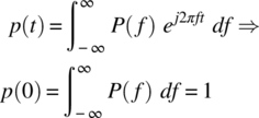
In Chapter 5 we considered the conversion of analog signals into digital by an ADC and baseband modulation techniques (see Figure 5.1). The line codes used for symbol transmission require infinite transmission bandwidth, as shown in Figure 5.26. Since frequency spectrum is a scarce resource, its economic use is of paramount importance. Therefore, the frequency components with negligible power of the transmitted signals are filtered out at the transmitter output.
On the other hand, in addition to the intended copy of the transmitted signal, its echos with different amplitude, phase and delay also arrive to the receiver. Hence, the original signal may be spread in time and frequency‐domains at the receiver input. On the other hand, the receiver filters out signals and noise outside its bandwidth for mitigating interference and noise. Therefore, the receiver should be able to cope with all these inconveniences to estimate the received pulses with minimum error.
This chapter will address the issues related to the reception of pulses at the receiver after transmission through a linear baseband channel.
6.1 The Channel
Let us consider the transmission of a pulse g(t) through a linear channel, as shown by Figure 6.1, characterized by its impulse response h(t) and the corresponding channel transfer function H(f). The signal x(t) at the channel ouput may be expressed as the convolution of the input pulse g(t) and the channel impulse response h(t). The output frequency response X(f) is the given by the product of the frequency responses G(f) and H(f). [1][2][3][4][5]
Figure 6.1 Transmission of a Pulse Through a Linear Channel.
Now let us assume that the channel impulse response is described by
where α denotes the channel gain and the time‐delay τ refers to the difference between the time the signal is injected into the channel and the time it is observed at the channel output. The signal at the channel ouput is then given by
The signal x(t) at the channel output, is the same as the transmitted pulse except for a finite time delay, which corresponds to the time required by the signal to go through the channel, and the channel gain, which accounts for the signal attenuation in the channel. Hence, x(t) has complete information of the transmitted pulse g(t) since its characteristics are preserved at the channel output. This channel is said to be ideal distortionless. In addition, the channel is said to be linear time‐invariant (LTI) if the channel gain α and the time‐delay τ do not vary with time. Taking the Fourier transform of both sides of (6.2) leads to
It is clear from (6.3) that the output spectrum X(f) is the same as that of the transmitted pulse except for a frequency-dependent phase shift due to delay τ and a constant channel gain α, which shows that all input frequency components are amplified/attenuated equally. Since time‐limited signals are not bandlimited, a channel providing ideal distortionless transmission requires infinite bandwidth (see (6.1) and Figure 6.2).
Figure 6.2 Infinite Bandwidth Requirement of an Ideal Distortionless Channel.
Now let us consider signal transmission through a low‐pass channel (with finite bandwidth). A low‐pass channel may be approximated by an ideal low‐pass filter (LPF) with a phase , accounting for the time delay in the channel. However, as shown in Figure 6.3 (see Figure 1.7), an ideal LPF channel provides a finite bandwidth but it is not causal. The non‐causality results from the fact that the bandlimited low‐pass channel starts responding before a signal is being applied at its input, that is, for t < 0. Therefore an ideal low‐pass channel is not realistic.
Figure 6.3 Non‐Causality in Ideal Low‐Pass Channel.
A channel whose frequency response deviates from that of an ideal LPF is dispersive. This implies that different frequency components of a pulse propagating through a dispersive channel are neither amplified/attenuated equally nor arrive with identical time delays. A dispersive channel causes intersymbol interference (ISI), that is, the interference between neighboring pulses. As we shall study in the following Sections, several techniques, for example, pulse shaping and equalization, are used to mitigate the ISI.
It should be clear from the above discussions that there is a trade‐off between the bandwidth and the duration of the impulse response (see Figure 6.3). Therefore, the non‐causality issue can be largely overcome in a low‐pass channel with a relatively flat bandwidth larger than W so as to allow undistorted transmission of the essential frequency components of a pulse. This corresponds to a channel impulse response which fades away more quickly in the time‐domain. Hence, pulse transmission through a low‐pass channel is affected not only by the channel bandwidth but also by the pulse bandwidth, , where T denotes the pulse duration. Therefore, low‐pass channels with sufficiently large and relatively flat passband and decaying rapidly for provide a good compromise between ISI and the bandwidth requirements.
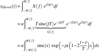
Note that a channel may also be dispersive, that is, an ISI channel, when the bandwidth of the pulse g(t) is wider than that of the low‐pass channel. Then, essential frequency components of the transmitted pulse remaining outside the channel bandwidth are filtered‐out by the channel. Hence, the pulse at the channel output becomes spread in time and causes ISI to preceding and following pulses. To have a better idea about the ISI imposed by the channel bandwidth, consider a pulse g(t) = 1 for 0 < t < T is applied at the channel input. The Fourier transform of this pulse G(f), given by (5.10), is obviously not bandlimited. If this pulse goes through a channel, which is modeled by an ideal LPF with bandwidth W,, then the low‐pass channel will filter out the frequency components of the pulse outside the filter bandwidth. Consequently, the signal at the output is found by low‐pass filtering X(f) given by (6.3) with G(f) from (5.10):
Figure 6.4 shows the original pulse g(t) = 1 for 0 < t < T and the filtered pulse, given by (6.4), for various values of the WT product for α = 1, τ = 0 and T = 1. WT = 1 implies that the filter (channel) bandwidth is equal to null‐to‐null bandwidth of the transmitted pulse and the original pulse corresponds to WT = ∞, hence infinite channel bandwidth. Note that the filtered pulse is spread in time and causes ISI even for large bandwidths of the low‐pass channel. Therefore, ISI is a serious problem in digital transmission systems.
Figure 6.4 Time‐Spreading of a Pulse Due to Band Limitation.
A multipath channel may also lead to dispersion of the signals in the time‐domain. A multipath channel refers to channel where multiple echos of the transmitted signal arrives to the receiver. The impulse response h(t) of a L‐path channel and the signal, x(t), at the channel output may be written as
Note that x(t) consists of weighted sum of replicas of the transmitted pulse g(t) where αk and τk denote, respectively, the complex gain and the delay of the kth path. Comparison of (6.1) and (6.5) shows that an ideal distortionless channel corresponds to signal propagation via a single path. As shown in Figure 6.5, the received pulse duration is spread in time and is longer than the original pulse duration. Consequently, the time‐spread received pulses interfere with each other, hence causing ISI. As the value of the maximum delay max{τk} increases in comparison with the pulse duration, the interference between neighboring pulses in time, becomes more serious. Unless the channel is LTI, αk and τk vary with time due to changes in the channel characteristics. The receiver suffers from destructive/constructive interference of multipath components as the time rate of change of the path gains increases in comparison with the pulse rate.
Figure 6.5 Time Spreading In a Multi‐Path Channel with Three‐Paths.
6.1.1 Additive White Gaussian Noise (AWGN) Channel
In the so‐called AWGN channel, the signal at the channel output may be written as in (6.2):
(6.6)
where w(t) denotes white Gaussian noise with zero‐mean and single‐sided PSD N0 and accounts for the receiver noise of usually thermal origin. In this ideal distortionless channel, the time delay τ can be ignored if the time that the signal is received by the receiver t = τ is taken as the reference. Similarly, the channel gain α can be omitted if the AWGN is scaled accordingly, so that the received signal‐to‐noise power ratio (SNR) remains the same. Consequently, a binary signal x(t) at the receiver input in an AWGN channel will simply be written hereafter as
(6.7)
In binary transmission, the sign A of the pulse amplitude is changed according to whether binary 1 or 0 is transmitted, for example, A = +1 for binary 1 and A = −1 for binary 0. Then, the receiver has the task of estimating the transmitted bit (1 or 0) corrupted by AWGN. The ability of the receiver to estimate the transmitted bit improves with increasing values of E/N0, which is defined by the ratio of the pulse energy E = A2T to the noise PSD N0.
The autocorrelation function of AWGN is given by
(6.8)
which implies that any two noise samples are uncorrelated unless they are sampled exactly at the same time. It is easy to show by Fourier transform relationship that the PSD of AWGN is flat, hence it is white (see Figure 6.6):
(6.9)
Figure 6.6 Autocorrelation Function and PSD of AWGN.
The AWGN is characterised by Gaussian pdf with zero mean and variance N0/2:
(6.10)
Figure 6.7 Pdf of the AWGN with Zero Mean and Unity Variance.
Figure 6.7 shows pictorially how the Gaussian pdf characterizes the random time‐variations in the AWGN.
In this chapter, the channel is characterized by AWGN, and dispersive, hence causing ISI. We will study the implications and devise methods to mitigate noise and ISI.
6.2 Matched Filter
Consider the detection by receiver of a pulse g(t) transmitted over an AWGN channel. The receiver is modeled as LTI filter of impulse response c(t). The filter input, x(t), is the output of the AWGN channel
(6.11)
where T denotes the pulse duration. Here, the transmitted pulse, g(t), which is an energy signal,
is corrupted by w(t), which denotes the sample function of a white noise process of zero mean and double‐sided PSD N0/2. The receiver is assumed to have the knowledge of the signal pulse shape g(t). In this Section, we will focus on the design of a receiver filter of impulse response c(t) which detects the pulse, g(t), in an optimum manner in an AWGN channel (see Figure 6.8). Here, optimum manner implies the maximization of the SNR at the receiver output at the sampling time t = T.
The signal at the matched‐filter receiver output is the convolution of x(t) and c(t):
(6.13)
The signal at the receiver output is sampled at time t = T, to estimate the transmitted signal. For a successful detection, we desire to maximize the received signal‐to‐noise ratio:
where |g0(T)|2 denotes the output signal power, and E[n2(T)] is the average output noise power at the sampling time t = T. Hence, the problem reduces to specifying c(t) which maximizes the output SNR.
Because g0(t) is the convolution of g(t) and c(t), the output signal power at t = T may be written in terms of the Fourier transforms of c(t) and g(t) as:
For a given a pulse shape g(t), hence G(f), the SNR in (6.17) can be maximized by determining the optimum frequency response Copt(f) of the matched filter. In order to maximize SNR in (6.17), we use Schwartz’s inequality for two finite‐energy signals u1(t) and u2(t):
Note from (6.22) that the maximum SNR SNRmax at the matched filter output depends only on the energy E of g(t) but not on its shape. This implies that all pulse waveforms having the same energy yield the same maximum SNR irrespective of their shapes. The pulse shape g(t) is chosen based on other considerations.
For example, the optimal impulse response copt(t) for a receiver filter matched to a pulse g(t) is shown in Figure 6.9. If c(t) is chosen to be optimum as in (6.21), then the optimum filter is said to be matched to the input signal, hence the matched‐filter.
Figure 6.9 Matching of the Receiver Filter to the Input Signal g(t).
The signal at the matched filter output may then be written as
(6.23)
Similarly, the average output noise power at the matched filter output is given by (6.16):
(6.24)
The energy of the matched filter receiver is usually normalized to unity:
One may infer from (6.26) that the matched filter output is a Gaussian random variable with mean value and variance N0/2.
Matched‐filter reception of a single pulse g(t) can be extended to receive binary 1 and 0 in a digital communication system. For example, signal waveforms s1(t) = g(t) and s2(t) = −g(t) may be used to transmit binary 1 and 0, respectively. The signals satisfying s2(t) = −s1(t) are said to be antipodal. For antipodal signals, the impulse response of the matched‐filter receiver may simply be taken as s1(T−t). The reception of binary signals may then be analyzed as above by simply noting that , where A and T denote, respectively, the amplitude and the duration of the pulse. Consequently, the positive sign of the matched filter output, , simply denotes that 1 is transmitted, and zero otherwise.
Figure 6.10 Matched Filter for a Rectangular Input Pulse.
6.2.1 Matched Filter Versus Correlation Receiver
Consider a correlation receiver which correlates the input signal with a normalized replica of the pulse, as shown in Figure 6.11. Here, as well, we choose as in (6.25) so that the input signal is correlated with a unit‐energy reference signal. The signal and the noise variance at the output of a correlation receiver are given by, at time t = T:
6.2.2 Error Probability For Matched‐Filtering in AWGN Channel.
Consider binary antipodal signaling where a binary symbol m1 is represented by + g(t), and a binary symbol m0 by –g(t). Note that m1 and m0 may represent binary symbols 1 and 0. It is assumed that the pulse g(t) has a duration Tb and an arbitrary shape, which is known to both transmitter and receiver. In an AWGN channel, the signal at the matched‐filter receiver input may be written as
(6.36)
where the noise w(t) has zero mean and a PSD of N0/2. The receiver consists of a matched filter, a sampler and a decision device as shown in Figure 6.15. Perfect synchronization is assumed between the transmitter and the receiver. This implies that the receiver is assumed to know the starting and ending times of transmitted pulses and the pulse shape, but not the polarity. The receiver is assumed to be matched to the transmit pulse g(t). Matched filter output is sampled at the end of each signalling interval. Given the noisy signal x(t) at its input, the receiver is required to make a decision, at the end of each signalling interval as to whether the transmitted symbol is m1 or m0. [1][3][4]
Figure 6.15 Receiver for Baseband Binary Antipodal Signals.
The sampled signal and the noise variance at the output of the matched filter is given by (6.26)
In view of (6.37), the matched filter output is a Gaussian random variable with mean , where Eb denotes the bit energy and the noise variance is (see Figure 6.16). Hence, the conditional pdf’s of the matched‐filter output y(Tb), when binary m1 and binary m0 are sent, are given by
Given the matched‐filter output (6.37), the decision device makes a decision as to whether m1 or m0 was transmitted, in the presence of the AWGN. The decision device compares the sample value y(Tb) to a preset threshold level λ:
Figure 6.16 Pdf of the Matched Filter Output When m1 or m0 is Transmitted.
Note that if there is no noise in the channel, then the pdfs in (6.38) reduce to delta functions:
(6.40)
Since the matched filter output can then assume only one of two values, , transmission is error‐free and the decision device makes no errors, as to whether binary symbols m1 or m0 was sent. However, in the presence of AWGN, the noise sample at the sampling instant, n(Tb), may change the sign of y(Tb) in (6.37) so that the decision device may make an erroneous decision. The decision error can be one of two kinds; the symbol m1 is chosen when m0 is transmitted, which is denoted by the probability p10, or symbol m0 is chosen when m1 is transmitted with probability p01 (see Figure 6.16).
Conditional probability of error p10, when symbol 0 was transmitted, is found as follows:
(6.41)
where Q is the so‐called Gaussian Q function (see (B.1)):
where p0 and p1 = 1−p0 denote respectively the a priori probability of transmitting m0 and m1. In most applications, a priory probabilities of transmitting 1 and 0 are equal to each other, that is, p0 = p1 = 0.5.
We now focus on determining the optimum value of the threshold λ in (6.44) which minimizes the average bit error probability. To achieve this, we differentiate P2 with respect to λ and equate to zero. Using the derivative of the Gaussian Q function
When symbols m1 and m0 are equiprobable, p0 = p1 = 1/2 (the so‐called binary symmetric channel, BSC), then λopt = 0. This implies that the optimum threshold is located at the midpoint between and , representing binary symbols m2 and m1. Then p01 = p10, and the average probability of bit error reduces to
which depends only on . Figure 6.17 shows that decreasing the noise variance and increasing the bit energy have similar effects in decreasing p10 and p01. Therefore, the average bit error probability depends only on γb, which is defined as the ratio of the bit energy to the noise variance. As the noise variance decreases and/or bit energy increases, the overlap between the tails of the two Gaussian pdf’s become less; this leads to lower bit error probabilities.
Figure 6.17 Effect of Increasing Noise Variance σn2 and the Energy Per Bit Eb on the Average Bit Error Probability for a Matched Filter Receiver.
Figure 6.18 shows the variation of the bit error probability with γb = Eb/N0. The Gaussian Q function, which is defined by (6.42), represents the area under the tail (between x and ∞) of a zero‐mean and unit variance Gaussian pdf (see Appendix B). Q(x) is a monotonically decreasing function of x with x(−∞) = 1, x(0) = 0.5, and Q(∞) = 0. Therefore the receiver exhibits an exponential improvement in P2 with increase in γb:
which implies that even a slight increase in γb leads to significant reduction in the bit error probability. For example, P2 = 1.91 10−4 for γb = 8 dB but reduces to 3.4 10−5 for γb = 9 dB.
Figure 6.19 Likelihood of m1 and m0 at the Matched‐Filter Output for Antipodal Signaling with Equiprobable Symbols with Bit Energies ± Eb in an AWGN Channel.
Figure 6.20 Matched Filter Receiver for Correlated Binary Input Signals.
Figure 6.21 Matched Filter Receiver for Two Orthogonal Signals s1(t) and s0(t).
Figure 6.22 Antipodal and Orthogonal Signals and Their Geometric Representations.
Figure 6.23 Matched Filter Receiver for Bi‐Orthogonal Signals.
6.3 Baseband M‐ary PAM Transmission
In binary PAM system (M = 2), equally likely and statistically independent bits 1 and 0 of duration Tb are represented by, for example, the amplitude levels +1 V and −1 V. The transmission rate is Rb = 1/Tb. The average transmit power level is 1 W over 1Ω resistance.
In quaternary PAM system (M = 4), the symbols, identified by dibits 00, 01, 11 and 10, are represented by one of the four amplitude levels, for example, −3 V, −1 V, +1 V and +3 V. Since the symbol duration is Ts = 2Tb, the symbol rate Rs = Rb/2 becomes one half of that for the binary PAM. However, the average transmit power level over 1Ω resistance is now (12 + 32)/2 = 5 W compared to 1 W for binary PAM, hence, 7 dB higher. Note that the selection of the 2 V difference between the amplitude levels in both 2‐PAM and 4‐PAM is not arbitrary. This selection ensures that, the minimum Euclidean distance and hence the error probability between neighboring amplitude levels are the same.
In M‐ary PAM, log2M bits are first grouped and the groups of log2M bits are converted into an M‐level PAM pulse train by using binary or Gray encoding. In M‐ary PAM, the symbol duration and symbol rate are given by Ts = Tb log2M and Rs = Rb/log2M, respectively. Hence, the symbol duration increases by a factor of log2M with respect to the binary PAM; the symbol rate (and the transmission bandwidth) decreases by the same factor.
Figure 6.24 depicts the representation of a binary bit sequence in binary and 8‐ary PAM. In 2‐PAM, binary 1’s and 0’s are represented by amplitude levels by +1 V and −1 V, respectively. In 8‐PAM, Gray encoding is used to transmit the same bit sequence, grouped in 3-bit symbols, 101 111 010 011 000 110 001 100 by sending +5 V, +7 V, −1 V, −3 V, −7 V, +1 V, −5 V and +3 V, respectively. The average transmit power of this signal is (52 + 72 + 12 + 32 + 72 + 12 + 52 + 32)/8 = 21 W (13.2 dBW). This implies that, in 8‐PAM, the three‐fold decrease in the symbol rate (transmission bandwidth) compared to the binary PAM is achieved at the expense of 13.2 dB increase in the transmit power.
M‐ary PAM signal is corrupted by noise and distortion over an AWGN channel. The received signal is passed through a matched filter and sampled in synchronism with the transmitter. Each sample is compared with appropriate thresholds so as to decide which symbol was transmitted.
Let us first consider a 4‐ary PAM system where the dibits 00, 01, 11 and 11 are represented by {am} = −3 V, −1 V, +1 V and +3 V, respectively, using Gray encoding. The signal transmitted by a 4‐ary PAM system may then be written as
(6.64)
where Ts = 2Tb and the pulse g(t) has energy E and duration Ts. The sampled output of a matched filter receiver may be written as (see (6.26))
where n(Ts) denotes AWGN noise with variance N0/2. Hence, the matched filter output, (6.65), is a Gaussian random variable with mean and variance N0/2.
Figure 6.25 shows the decision variable given by (6.65) for the considered 4‐PAM constellation and the decision thresholds. The pdf of the decision variable is also shown when s3 is transmmitted. The symbol s3 will be erroneously received when or . Because of the symmetry of the Gaussian pdf, one has
Figure 6.25 Decision Variable for the 4‐PAM Signal Constellation with Gray Encoding.
It is obvious from Figure 6.25 that the probability of error for symbols s2 and s3 is equal to 2p, but it is equal to p for the symbols s1 and s4. Therefore, the average symbol error probability for 4‐ary PAM is simply 6p averaged over four symbols:
(6.67)
In M‐ary PAM, when either one of the two outside levels ± (M−1) is transmitted, an error occurs in one direction only. For other amplitudes, the error occurs in two directions. Therefore, the average symbol error probability for M‐ary PAM is given by
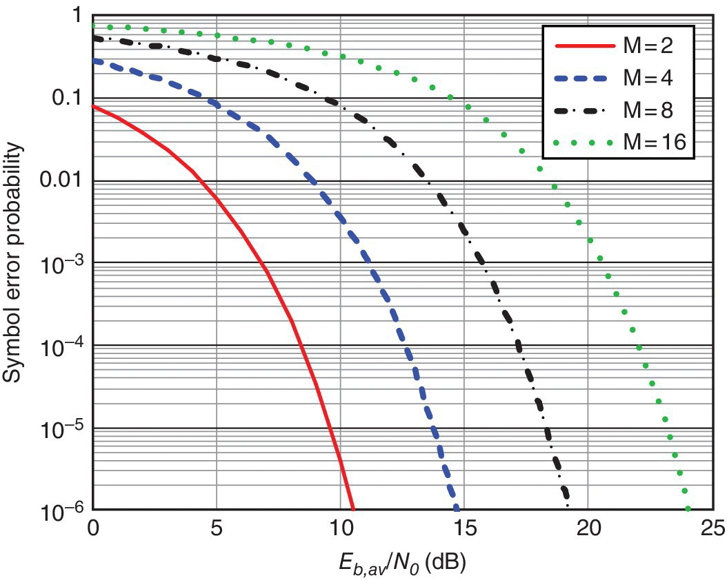
Symbol error probability for M‐ary PAM is shown in Figure 6.26 for M = 2, 4, 8 and 16. The error performance for binary PAM is identical to that for matched‐filter reception of antipodal signals (see Figure 5.34, (5.51) and (6.47)). The bit error probability for M‐PAM with Gray encoding may be found by dividing (6.70) by the number of bits log2M per PAM symbol.
The effect of the alphabet size M on the symbol error performance is usually studied in terms of the required Eb/N0 for a given value of the symbol error probability. This implies that the argument of the Q function should remain the same for all values of M, ignoring the terms in front of the Q function in (6.70). Therefore, for achieving the same symbol error probability, the bit energy of M‐ary PAM should be increased by
(6.71)
compared to the binary PAM. As shown in Table 6.1, for a given symbol error probability, the required average bit energy should be increased by about 4 dB when M is doubled. For a given symbol error probability and bit rate, the 8‐PAM requires 8.45 dB higher average bit energy but one‐third of the transmission bandwidth compared to binary PAM. Conversely, for a given channel bandwidth (i.e., a given symbol rate Rs), the transmitted bit rate by M‐ary PAM is Rb/Rs = log2M faster than the corresponding binary PAM. For example, the bit rate increases by a factor of 3 for 8‐ary PAM compared to binary PAM.
Figure 6.26 Symbol Error Probability of M‐ary PAM Versus Eb,av/N0 (dB).
Table 6.1 For a Given Symbol Error Probability, the Increase in the Required Average Bit Energy and the Corresponding Decrease in Symbol Rate with the Number of Amplitude levels M.
M
Rs/Rb
2
1 (0 dB)
1
4
2.5 (4 dB)
1/2
8
7 (8.45 dB)
1/3
16
21.25 (13.27 dB)
1/4
32
68.2 (18.34 dB)
1/5
The required average bit energy to achieve a given symbol error probability in PAM systems increases as the alphabet size M increases. Therefore, higher peak transmit powers are needed with increasing M values. For M‐ary PAM, the required peak transmit power is given by
The peak‐to‐average power ratio (PAPR) for M‐ary PAM is thus given by
(6.74)
which changes between 1 and 3 as M goes from 2 to infinity. This means that in M‐ary PAM systems, the peak power can be at most 3 times as large as the average transmit power. Also note from (6.72) and (6.73) that the average and peak powers do not depend on the transmission rate.
6.4 Intersymbol Interference
At the beginning of this Chapter, we discussed the physical mechanisms, for example, bandwidth limitation and multipath propagation, by which ISI occurs in communication systems. Here, we will study how ISI degrades the system performance and how this degradation can be mitigated.
Consider a baseband binary PCM system, which consists of a transmitter, AWGN channel and a receiver, as shown in Figure 6.27. The input binary sequence {bk} consists of equally‐likely binary digits 1 and 0, each of duration Tb. Pulse amplitude modulator converts the input pulse sequence into a new sequence {ak} of electrical symbols as follows:
Signal s(t) undergoes attenuation, phase changes and distortion as it goes through the channel of impulse response h(t). The signal x(t) at the receiver input is simply given by the convolution of the input signal with the channel transfer function:
(6.81)
where w(t) denotes the AWGN with zero‐mean and two‐sided PSD N0/2. The signal at the receive filter output is given by the convolution of the noisy signal x(t) with the impulse response c(t) of the receive filter:
Here, n(t) denotes the AWGN filtered by the receiver filter with impulse response c(t). On the other hand, the pulse p(t) is proportional to the time convolution of the impulse responses of the transmit filter, the channel and the receive filter. Note that μ is a scaling factor since p(t) is normalized to unity at t = 0
(6.84)
Ideally, apart from the noise term, the received signal in (6.82) is desired to be the same as the transmitted signal given by (6.80). One can observe from (6.83) that this possible only if h(t) and c(t) can be represented as delta functions. However, this is not realistic since it requires infinite channel bandwidth. Comparison of (6.80) and (6.82) shows that, due to the convolution process defined by (6.83), p(t) ≠ g(t). Therefore, p(t) is a time‐spread version of g(t), hence undergoes time dispersion and ISI.
The transmitted data sequence is estimated by the decision device shown in Figure 6.27. Amplitude of each sample is compared to a threshold λ; if y(iT) > λ, then a decision is made in favor of 1, otherwise, the decision is made in favor of 0.
Figure 6.28 A Simplified Block Diagram of a Communication System with a Multipath Channel Leading to ISI.
Figure 6.29 Effect of Two‐Path Transmission on the Bit Error Probability.
6.4.1 Optimum Transmit and Receive Filters in an Equalized Channel
Channel equalization is one of the alternative techniques for ISI mitigation. In the equalization process, the coherent receiver determines frequency response Heq(f) of the equalization filter from the estimate, Ĥ(f), of the channel frequency response and neutralizes the effects of non‐ideal channel frequency response, as shown in Figure 6.30. For equalizing the channel, the coherent receiver should be equipped with a device that predicts the channel impulse response (hence, the transfer function).
Figure 6.30 Effective Frequency Response μP(f) = G(f)H(f)Heq(f)C(f) of the Equalized Channel.
In the presence of the equalization filter, (6.83) and its Fourier transform may be written as
The optimum receiver is then matched to the transmit pulse, copt(t) = kg*(T−t) as in (6.21), so as to maximize the output SNR. In view of (6.92), this also implies that the transfer functions of transmit and receive filters may be chosen to be proportional to that of a particular P(f):
where ∝ denotes proportionality. One may observe from (6.93) that transmit and receive filters should have the same (frequency and time) characteristics. This is obviously a desired result for duplex transmission. Nevertheless, we still need an answer as to the determination of P(f). A suitable choice of the line code described by g(t), and a receive filter c(t) matched to g(t) maximizes the output SNR in an equalized channel. We know from match‐filter reception that there is no limitation about the shape of g(t) for SNR maximization. Therefore, it is logical to ask if ISI can be mitigated by a clever choice of g(t), hence p(t). This question will be addressed in the next Section.
6.5 Nyquist Criterion for Distortionless Baseband Binary Transmission In a ISI Channel
In the previous section, we considered the equalization of a dispersive channel causing ISI. In this section, we also consider a memoryless dispersive channel, with transfer function H(f) ≠ 1 , but with no equalization. Hence, for a dispersive and unequalized channel, we will determine optimum impulse response of p(t) (also those of transmit and receive filters g(t) and c(t)) in order to eliminate the ISI and to minimize the bit error probability (see Figure 6.31). Note that each symbol is decoded separately in a memoryless channel since the neighboring symbols in time are independent from each other. Minimization of the bit error probability implies the use matched filter at the receiver. On the other hand, based on the assumption of duplex transmission, each side acts both as transmitter and receiver. Therefore, impulse responses g(t) and c(t) for transmitter and the receiver should be the same.
When the synchronization is perfect between transmitter and receiver, the receive filter output y(t) in Figure 6.27 is sampled synchronously with the transmitter. The receive filter output (6.82), sampled at ti = iT, may be written as
where µai denotes the contribution of the ith transmitted bit and represents the received bit in the absence of noise and ISI. The second term in (6.98) accounts for the ISI due to time dispersion. Note that the term , which denotes the value of kth pulse (to transmit ak) at the sampling time ti = iT, accounts for the ISI caused to ai by the kth pulse. It is thus evident that not only the AWGN but also the ISI contributes to the bit error probability.
The ISI at the receiver output vanishes if in (6.98) becomes zero for all non‐zero values of i‐k:
As the matched‐filter receiver c(t) will be matched to the effective pulse at the receiver input, , that is, . Then, using (1.12) and (6.83)μ may be shown to be equal to the square root of the energy of the ith pulse, and the variance of n[iT] is given by N0/2 (see (6.26)):
(6.101)
Hence, the SNR at the receiver output is , as expected.
To determine the implication of (6.100) on the frequency domain characterization of p(t), we rewrite, using (5.1)–(5.3), the expressions for the instantaneously sampled version of p(t) and its Fourier transform:
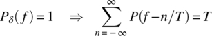
As shown in Figure 6.31, P(f) denotes the transfer function of the overall system and hence incorporates the transmit filter, the channel and the receive filter. On the other hand, (6.104) implies ISI‐free transmission if the sum of the copies of P(f) separated by 1/T in the frequency domain is equal to T, independently of the frequency. This is called the Nyquist criterion, which is shown pictorially in Figure 6.32 for two different P(f)’s. In summary, the ISI will be eliminated and the output SNR will be maximized in a memoryless dispersive channel, if P(f) is chosen so as to satisfy (6.104), and C(f) and G(f) are related to P(f) as in (6.93). Below, we will investigate several alternative P(f)’s that satisfy (6.104).
Figure 6.32 Nyquist Criterion for Eliminating ISI.
6.5.1 Ideal Nyquist Filter
One of the the simplest ways to satisfy the zero‐ISI condition, given by (6.104), is to choose P(f) as
which is shown in Figure 6.33 and Figure 6.32 with continuous lines. Since T = 1/(2W), the bandwidth W of the so‐called ideal Nyquist channel can support a symbol rate Rs = 1/T:
Ideal Nyquist channel allows a transmission rate of Rs = fs = 2 W, which is equal to the sampling rate fs and twice the channel bandwidth W, also known as the Nyquist bandwidth. The resulting spectrum efficiency Rs/W = 2 represents the highest available spectrum efficiency and hence the maximum transmission rate provided by all possible P(f)’s. In other words, Nyquist channel allows for zero ISI transmission with minimum channel bandwidth.
As shown in Figure 6.33, the corresponding time pulse pN(t), defined by (6.105), is equal to unity at t = 0 and vanishes at t = iT, i ≠ 0; hence it satisfies (6.99). However, PN(f) being band‐limited to W, pN(t) is non‐causal since it is not time‐limited. Non‐causality exhibits itself by the requirement for starting to send the pulse pN(t) at t = −∞ instead of at t = 0. On the other hand, pN(t) has a slow decay rate with time and decreases as 1/|t| for large t. Consequently, pN(t) may have unacceptably large values even at times largely separated from the transmission time, t = 0. This causes nonnegligible ISI when sampling times deviate from iT due to synchronization errors.
Figure 6.33 Ideal Nyquist Filter and Ideal Nyquist Pulse Where W = 1/(2 T) = Rs/2. Sampling times are shown by circles.
Figure 6.34 shows the time variation of the signal for transmitting the bit sequence 1001011 by using ideal Nyquist pulse. The binary 1 is transmitted by +1 V amplitude while −1 V amplitude is used for transmitting a binary 0. Because pN(0) = 1 and pN(iT) = 0 for i ≠ 0, the pulses used for transmitting the bit sequence do not interfere with each other at t = iTb, hence an ISI‐free transmission. Since the envelope of the sinc pulse given by (6.105) decays as 1/t with time, ISI occurs if the receiver, with timing errors, does not sample the incoming signal at exactly iT. Hence, an ISI‐free transmission requires a receiver which is perfectly time‐synchronized with the incoming signal sequence and an ISI‐free pulse shape, defined by (6.104), which decays rapidly with time. On the other hand, Figure 6.34 clearly shows that one should start transmitting the pulse pN(t−iT) well ahead of the transmission time t = iT of the bit that it represents; hence, pN(t) is not causal. From the frequency domain perspective, the ideal Nyquist channel requires an ideal low‐pass channel, that is, flat frequency response in [−W to W] and zero elsewhere, which is physically unrealizable.
Figure 6.34 Transmission of a Binary Sequence Using Ideal Nyquist Pulse.
Figure 6.35 The Block Diagram of the M‐ary PCM System Considered.
6.5.2 Raised‐Cosine Filter
We have shown above that the ideal Nyquist filter, defined by (6.105), satisfies the zero‐ISI condition, given by (6.104). It is easy to show that the raised cosine spectrum, defined by
also satisfies the zero‐ISI condition, as shown in Figure 6.36 and Figure 6.32 in dash‐lines. The frequency spectrum of the raised‐cosine pulse and the corresponding pulse waveform are shown in Figure 6.36. As its name implies the frequency spectrum of the raised‐cosine filter consists of a cosine curve raised so that it always assumes positive values. The so‐called roll‐off factor α changes between 0 and 1 and is used as a measure of the bandwidth in excess of the bandwidth of the ideal Nyquist filter (W = Rs/2). The transmission bandwidth of a raised‐cosine filter is given by
The transmission bandwidth B changes between W and 2 W by adjusting the roll‐off factor between 0 and 1.
Figure 6.36 Raised‐Cosine Filter and Raised‐Cosine Pulse Where W = 1/(2 T) = Rs/2. circles show the sampling times.
The time pulse of raised‐cosine filter is found by the inverse Fourier transform of PRC(f):
(6.111)
where the factor sinc(2Wt) characterizes the ideal Nyquist pulse and ensures zero crossings of p(t) at the desired sampling instants of time t = iT. The second factor decreases as 1/t2 and ensures that the decay rate of the raised‐cosine pulse is faster than that of the ideal Nyquist pulse. Hence, raised‐cosine pulse is less susceptible to timing errors. On the other hand, ISI due to timing errors decreases as α increases from 0 (B = W) to 1 (B = 2 W), as expected. Hence, raised‐cosine filtering eliminates ISI more effectively than Nyquist filtering at the expense of a controlled increase in the transmission bandwidth.
At t = ±T/2 = ±1/4 W, we have pRC(t) = 0.5, that is, pulse width at half amplitude is equal to bit duration T. There are zero crossings at t = ±3 T/2, ±5 T/2 in addition to usual crossings at t = ±T, ±2 T…
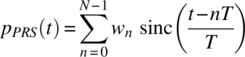
In addition to the ideal Nyquist and raised‐cosine filters, correlative level coding may also be used to remove the ISI. In this method, which is also called as the partial‐response signalling (PRS), ISI is introduced to the transmitted signal in a controlled manner. Using this information, the ISI induced by the channel is removed at the receiver. Signalling rate achieved by PRS is equal to the Nyquist rate (2 W symbols per second) in a channel of bandwidth W Hz.
Consider an input binary sequence {bk} of uncorrelated binary symbols 1 and 0, each of duration T. This sequence is applied to a binary pulse‐amplitude modulator, producing
(6.117)
Two‐level sequence {ak} is first passed through a simple filter involving a single delay element and a summer, as shown in Figure 6.37. The output of the so‐called duobinary encoder,
has three levels, ±2 and 0, depending on the combinations of ak and ak−1. Input sequence {ak} of uncorrelated two‐level pulses is thus transformed into a sequence {ck} of correlated three‐level pulses. The correlation between ck’s, introduced under designer’s control, is exploited by the receiver to remove the ISI caused by the channel.
Using the frequency response of ideal Nyquist channel of bandwidth W = 1/2 T given by (6.105), the overall frequency response of duobinary signalling may simply be written as
Hence, unlike the frequency response of ideal Nyquist filtering, the PSD of duobinary signaling is not flat (see Figure 6.38) but the required bandwidth is the same as that for ideal Nyquist filter, that is, W = 1/(2 T) = Rs/2.
From Figure 6.37 and (6.119), the impulse response for duobinary signaling is found as
Note that the response to an input pulse at t = 0 is partial (see Figure 6.38), that is, the response is spread over two signalling intervals, at t = 0 and t = T, hence partial response signaling. On the other hand, the impulse response, given by (6.121), which is the Fourier transform of the cosine‐type transfer function, decays as 1/t2, that is, faster than the ideal Nyquist pulse.
Figure 6.38 Duobinary Filter and Duobinary Pulse Where W = 1/(2 T). Sampling points are shown by circles.
The original two‐level sequence {ak} may be detected from the duobinary‐coded sequence {ck} using (6.118). If represents the estimate of the pulse ak by the receiver at time t = kT, then subtracting the previous estimate from ck, one gets . If ck is received correctly and the previous estimate is correct, then the current estimate âk is also correct. Otherwise, will be incorrect and, once an error is made, it propagates through the output. Hence, the error propagation is the major drawback of this detection procedure.
Propagation of errors can be avoided by using precoding before duobinary encoder as shown in Figure 6.39. Precoding (differential encoding) converts the binary data sequence {bk} into another binary sequence {dk} by, for example, . Precoded data sequence is thus given by
The receiver for decoding the duobinary encoded sequence is simple. In view of (6.124), the receiver for duobinary signalling consists of a rectifier, which takes the absolute value of the received signal sequence {ck} and a detector, which compares the rectifier output to a threshold level of 1 to estimate the transmitted bit:
This detector requires no knowledge of any input sample other than the present one. Hence, neither error propagation nor ISI can occur in this detector.
Table 6.2 Process of Duobinary Encoding of the Binary Sequence {0010110} with Precoding.
In an AWGN channel, matched filter output of the received duobinary‐encoded bit sequence may be written from (6.124) as
(6.126)
where wk denotes the sample of a zero mean Gaussian random variable with variance σ2 during the period of the kth symbol. From the decision rule given by (6.125) and the decision regions shown in Figure 6.40, one infers that an error occurs if when bk = 1 is transmitted and if when bk = 0 is transmitted:
(6.127)
Figure 6.40 Decision Regions for Duobinary Signaling for Equiprobable 1’s and 0’s.
Assuming that , the average probability of error for duobinary signalling is found to be
(6.128)
The average bit energy and the noise variance at the output of the transmitting filter G(f) are given by
where is assumed (see (6.93)). The SNR for dubinary signalling may then be written as follows:
(6.130)
Ignoring the 3/2 factor multiplying the Q function in P2 expression for duobinary signaling in (6.129), the degradation in SNR compared to binary signalling is 2.1 dB. However, the 2.1 dB SNR degradation in duobinary signaling is paid for removing the ISI and transmitting at the Nyquist rate.
6.6.2 Generalized Form of Partial Response Signaling (PRS)
As described by (6.118), duobinary signaling uses the two consecutive bits to deliberately insert correlation into the transmitted bit sequence, which is exploited by the receiver to remove the ISI introduced by the channel. This concept can be generalized to other schemes known as correlative level coding or PRS by taking correlation spans more than two binary digits:
where {wn} denote the weight coefficients. Block diagram of a generalized correlative level encoder is shown in Figure 6.41.
Figure 6.41 Generalized Form of Partial Response Signaling.
The use of (6.134) leads to different classes of partial response signalling schemes with pulses which may be expressed as a weighted linear combination of N ideal Nyquist pulses (see (6.121)):
In view of (6.118) and (6.134) (also compare (6.121) and (6.135)), duobinary signalling is described by N = 2, and the coefficients w0 = w1 = +1.
With PRS, binary transmission is possible over baseband channels at the Nyquist rate. Different spectral shapes with gradual cut‐off characteristics can be produced. However, larger SNR’s are needed for the same error probability compared to corresponding binary PAM systems.
Table 6.3 provides a summary of several pulses used for ISI mitigation in comparison with the commonly used NRZ pulse. Note that Nyquist and duobinary pulses operate at minimum transmission bandwidth W = 1/(2 T) and induce no ISI. However, duobinary signalling requires 2.1 dB higher SNR compared to the binary signalling. On the other hand, the transmission bandwidth B = W(1 + α) of the raised‐cosine pulse is determined by the roll‐off parameter α, 0 < α < 1. The increase in the transmission bandwidth is paid by higher robustness to timing/synchronization errors. The raised‐cosine pulse reduces to the Nyquist pulse for α = 0.
Table 6.3 Comparison of Transmission Bandwidth of Various Signaling Pulses.
Pulse type
Time pulse, p(t)
Frequency transfer function, P(f)
Bandwidth, W
ISI
Nyquist
T rect(f T)
1/(2T)
No
Raised cosine
(1+α)/(2T)
No
Duobinary
1/(2T)
No
NRZ
rect(t/T)
T sin c(f T)
null‐null: 2/T B3dB = 0.89/T
Yes
Homework 6.3 Modified duobinary signaling
Modified duobinary signaling is described by N = 3, w0 = 1, w1 = 0, and w2 = −1. Determine anaytical expressions for the time pulse and the frequency response for this signaling. Determine the required transmission bandwidth. Also formulate the decision rule at the receiver output.
6.7 Equalization in Digital Transmission Systems
In an AWGN channel, a matched filter receiver is known to be optimal in the sense that it maximizes the output SNR, and minimizes the bit error probability. The impulse response of a matched filter is a time reversed and delayed version of the input pulse, hence matched to the input pulse.
In a dispersive channel, transmitted pulses are spread in time, leading to ISI and increased bit errors at the receiver. Equalization is a technique to combat ISI in dispersive channels. An equalizer is actually an inverse filter of the channel, which is inserted at the receiver input to compensate for the fluctuations in the channel amplitude, phase and delay characteristics. In the so‐called frequency selective channels, where the channel transfer function is frequency‐dependent. An equalizer enhances (attenuates) the frequency components with small (large) amplitudes in the received signal in order to provide a flat received frequency response and a linear phase response. For time‐selective channels, an adaptive equalizer is designed to track the channel variations so as to satisfy the above requirements.
Among the most commonly known equalizers is a zero‐forcing equalizer which can be implemented as a FIR filter. The taps of a zero‐forcing equalizer are adjusted such that the equalizer output is forced to be zero at a finite number of sample points on each side of the received pulse, ignoring the channel noise. Consequently, the performance of a zero‐forcing equalizer degrades as the channel becomes more noisy. However, the taps of the so‐called minimum mean‐square error (MMSE) equalizer are adjusted such that the mean‐square error (MSE) between the equalizer output and the desired signal is minimized. The MMSE equalizer outperforms zero‐forcing equalizer since it takes into account the effects of both ISI and channel noise.
Note, however, that channel equalization only cannot remove the ISI caused by the transceivers. Therefore, pulse shaping may be required, In a channel with ISI acting only (i.e., ignoring the channel noise), the choices of Nyquist, raised‐cosine or partial‐response signaling (PRS) would force the resulting ISI to be zero at sampling instants nT, n > 0, except for at n = 0 where the symbol of interest occurs. A linear receiver implemented as a zero‐forcing equalizer is followed by a decision‐making device. Symbol‐by‐symbol detection is then optimal.
In practice, the channel noise and the ISI act together on a data transmission system. Then, design of a linear receiver should be optimized for the general case of a linear channel that is both dispersive and noisy. The optimum linear receiver then consists of the cascade connection of a matched filter, and a transversal (tapped‐delay‐line) equalizer, with tap spacing equal to the bit duration. Table 6.4 shows a summary of the channels considered, the approaches for removing ISI and the required transmission bandwidth.
Table 6.4 Equalization Strategies in ISI Only and ISI and AWGN Channels.
Interference
Solution
Characteristics
Noise only
Matched filter receiver
SNR = 2Eb/N0
ISI only
Zero‐forcing receiver
Nyquist: B = W RC: B = W(1 + α) PRS: B = W, higher Tx power
Noise + ISI
Matched filter + equalizer optimized in MMSE sense
Adaptive for time‐variant chanels
Figure 6.42 Equalizer and Matched Filter in a Multipath Channel.
Figure 6.44 Effect of the Residual ISI Term in the Output SNR of a Zero‐Forcing Equalizer.
References
[1] S. Haykin, Communication Systems (3rd ed.), John Wiley: New York, 1994.
[2] J. G. Proakis and M. Salahi, Communication Systems Engineering (2nd ed.), Prentice Hall: New Jersey, 2002.
[3] A. B. Carlson, P. B. Crilly, and J. C. Rutledge, Communication Systems (4th ed.), McGraw Hill, Boston, 2002.
[4] B. Sklar, Digital communications, Fundamentals and Applications (2nd ed.), Prentice Hall: New Jersey, 2003.
[5] I. A. Glover, and P. M. Grant, Digital Communications (2nd ed.), Pearson Prentice Hall: Harlow, 2004.
Problems
Consider the following binary signalling schemes with equiprobable signals:
where A is a constant.
For each of the above each of the above signalling schemes:
Determine the correlation coefficient between the two signals.
Give the structure of the matched‐filter.
Draw the signal‐space diagram related to the matched‐filter output.
Determine the optimal decision threshold level.
Determine the probability of error.
Binary data is transmitted by using a pulse g(t) for 0 and a pulse Ag(t) for 1. The energy of the pulse g(t) is equal to E and A can be positive or negative number.
Draw the block diagram of a matched filter receiver used for optimal detection of this signalling scheme,
Determine the optimum impulse response of the matched filter,
Determine the optimum detection threshold if 0 and 1 are not equally likely.
Determine the probability of error if 0 and 1 are not equally likely.
Is the choice of the pulses g(t) and Ag(t) a good one? Explain why. Discuss the implications of this choice on the total transmit power of the transmitter. How can the probability of error be minimized in this system?
A matched filter is used for the reception of the pulse in an AWGN channel with zero mean and PSD N0/2 W/Hz.
Find and sketch the impulse response of the filter which is matched to the pulse g(t).
Derive an expression for the maximum output SNR in terms of the parameters α, T and N0.
Consider the signalling scheme characterized by s0(t) = −g(t) and s1(t) = g(t) for 0 ≤ t ≤ T, with equal probability, in a AWGN channel with PSD N0/2 watts/Hz. Sketch the pdf of the decision variable corresponding to s0(t) and s1(t), and derive the probability of error.
Repeat (a)–(c) for g(t) = 2 t/T, 0 ≤ t ≤ T.
An antipodal binary signalling scheme uses equiprobable pulses with amplitudes + A and −A during the interval (0, T) in an AWGN channel with single‐sided PSD of N0. Assume that the received signal is detected with a matched filter:
Write down the expression for the Pb at the matched filter output.
Express the maximum data rate that can be transmitted with a Pb less than or equal to 10−6 in terms of A, T and N0.
Determine the SNR at the matched filter output and the corresponding bit rate for A = 1 mV and N0 = 10−12 W/Hz.
In an antipodal system, is sent for bit 0 and A for bit 1. The probability of transmitting a bit 0 is p0 and p1 for 1. The matched filter output is characterized by where E denotes the bit energy and n is the noise sample with an exponential distribution:
Here, σ denotes the rms‐value of the noise.
Using the equality , for , determine the optimum decision threshold.
Determine the average error probability.
Calculate the SNR in dB required for the error probability , assuming p0 = p1.
Repeat (c) when the noise is Gaussian instead of being exponentially distributed. Discuss whether Gaussian noise or the exponentially distributed noise is more favorable for the system performance.
Consider matched‐filter reception of the two signals s1(t) and s2(t) as given below:
where A is a constant and T denotes the symbol duration.
Determine the transmitted signal energies for binary symbols 1 and 0.
Are these signals correlated? If so, determine the correlation coefficient between these signals.
Draw the block diagram of a matched‐filter receiver for these two signals, using matched filters with unit energy. Write down the analytic expressions at appropriate points when the input signal is s1(t) + w(t), where w(t) is AWGN with zero mean and variance N0/2.
Determine the average SNR at the output of the matched filter receiver.
Determine the average bit error rate when s1(t) is sent for binary 1 and s2(t) is sent for binary 0.
A binary digital communication system uses the following signalling scheme for information transmission:
Draw the block diagram of the optimum receiver for an AWGN channel with one‐sided PSD N0, assuming that the probability of transmitting 0 and 1 is p0 = p1 = 0.5. Write down the output of the optimum receiver when 1 and 0 are sent.
Derive analytically the optimum threshold, assuming that the probability of transmitting 0 and 1 are p0 = 0.4 and p1 = 0.6.
Derive analytically the probability of error for the special case of p0 = p1 = 0.5. Compare the BER performance of this system with antipodal signaling.
Consider a binary orthogonal signalling system where Eb denotes the energy for each of the waveforms. The two signals are thus defined as
Assuming that s1 was transmitted in an AWGN channel with zero mean and noise variance N0/2, write down the observation vector, x = (x1 x2), at the output of the demodulator.
Write down the pdf’s of x1 and x2.
Determine the probability of error when s1 and s2 was transmitted. Determine the total probability of error, assuming that s1 and s2 are equiprobable.
Determine the total probability of error when s1 and s2 are defined as below.
Consider that Fourier transform of a time waveform is given by H(f) = T sinc2(fT).
Determine the impulse response h(t) corresponding to H(f).
Determine the impulse response of the filter matched to h(t).
Determine the output of the matched filter at the sampling instant t = T.
A pulse shaping circuit is defined by the following impulse response:
Determine and plot the frequency response corresponding to h(t).
Determine and plot the frequency response corresponding to h(t) ⊗ pN(t), where pN(t) denotes the time waveform of the Nyquist pulse. Determine time pulse and explain if the resulting pulse can be categorized as a PRS pulse.
Determine and plot the frequency response corresponding to h(t) ⊗ p0(t), where p0(t) denotes the time waveform corresponding to P0(f) = 1/sinc(fT). Discuss relative advantages and disadvantages of the waveforms obtained in (a), (b) and (c).
The figure below shows a signalling scheme with signals s1(t) and s0(t) in an AWGN channel of zero‐mean and PSD N0/2.
Design a matched‐filter receiver that decides in favour of signals s1(t) and s0(t) over the observation interval 0 ≤ t ≤ 3 T, assuming that these two signals are equiprobable. Determine the corresponding error probability at the receiver output.
Now assuming that s1(t) and s0(t) both carry three bits over the observation interval 0 ≤ t ≤ 3 T, design a matched‐filter receiver that decides in favour of each of the equiprobable bits carried by s1(t) and s0(t) over (i‐1)T ≤ t ≤ iT. Determine the corresponding error probability at the receiver output.
A binary signaling has the conditional probability density functions fY(y|mi) at the matched filter output as shown below:
Assume that the probability of transmitting the signal mi is pi, i = 1,2.
For a given decision threshold level of λ, determine the conditional probability of error when mi, i = 0,1 is transmitted. Determine the average probability of error.
Determine the optimum decision threshold level and the corresponding average probability of error.
Assuming that p1 = 0.6 and p2 = 0.4, plot the average probability of error for –0.2 < λ < 0.2 and compare with that obtained for the optimal case.
Determine the average error probability for p1 = p2 = 0.5 and compare with the result you obtained in part (b).
A ternary signal configuration at the matched‐filter output in an AWGN channel is shown below:
If p(s0) = p(s1) = p(s−1) = 1/3, determine the optimum decision regions and the corresponding error probability of the optimum receiver.
Repeat part (a) for p(s0) = 0.5, p(s1) = 0.2, and p(s−1) = 0.3.
Repeat part (a) for p(s0) = 0.5, p(s1) = 0.25, and p(s−1) = 0.25. Compare your results with those in part (a) and (b).
The detector following a matched‐filter demodulator faces the following hypothesis‐testing problem:
where H1 and H0 correspond to the transmission of binary symbols m1 and m0, with p(H1) = p, and p(H0) = 1‐p. Eb denotes the bit energy and w(T) is the sampled Gaussian random variable with zero mean and variance σ2. The maximum a posteriori (MAP) rule for deciding whether H1 or H0 is transmitted may be written from (6.51) as where fZ(z|H1) and fZ(z|H0) denote the conditional pdf’s.
Formulate the MAP test to determine whether H1 or H0 is transmitted.
Determine an expression for the probability of error for p = 1/2.
Repeat (a) for p = 1/2 when the MAP decision is based on the transmission of the same symbol L times (repetition coding), instead of only once. Compare the performance of this test to the one in (a).
In some applications, the noise at the demodulator input may not have a flat PSD. The noise with non‐flat PSD is called as colored noise (not being white). In such cases, a whitening filter is inserted prior to the receiver in order to whiten the colored noise. Consider that the noise at the receiver input is Gaussian but with a nonwhite PSD, Gn(f). The transfer function Hw(f) of the whitening filter is chosen so that the noise w(t) at its output is white with double‐sided PSD N0/2:
where n(t) is the zero‐mean colored noise with the PSD given by Gn(f).
Assume that the whitening filter is a real‐valued filter and represent the output of the whitening filter when the input pulse is s(t). Finally, y(t) and w0(t) represent the responses of the optimum matched filter hopt(t) to and w(t), respectively.
Determine the frequency response of the whitening filter Hw(f).
If h(t) is matched to , determine the noise power, signal power and the SNR at the detector input, that is, .
Consider that a baseband binary signal and additive colored noise is received by a matched filter. Due to the use of the whitening filter as in Problem 6.15, the rest of the receiver must be matched to the distorted signaling waveforms at the output of the whitening filter, that is, .
Assuming that s1(t) and s0(t) are correlated, show that the signal energy at the matched filter receiver output may be written as follows:
where and T denotes the symbol duration.
Show that the SNR at the matched filter output is given by
Hint: If is real, then
The binary data stream {1011100101} is applied to the input of a duabinary encoder.
Give the duobinary encoder output and corresponding receiver outputs, without using a precoder.
Assuming that the fourth bit is erroneously received as 0, determine the new receiver output.
Repeat (a) and (b) when a precoder is used.
Consider the following demodulated (modified) duobinary data stream: {2 2 0 0 –2 0 2 0 0 0 –2 0}
Decode the received stream, assuming it is duobinary. State if there is any error in the demodulated stream. Can you estimate the correct transmitted digit sequence? Is there a single correct data stream?
Repeat (a) assuming that the above stream is modified duobinary.
Consider that a pulse + g(t) is sent for binary 1 and –g(t) for 0. The rectangular pulse g(t) is defined by
The channel impulse response is given by
where Tm > Tb.
Plot the signal at the channel output when the input is a binary 1.
Illustrate the effect of ISI when the input bit sequence is 011.
What is the impulse response of the optimim matched filter for this signal.
Plot the time variation of the matched‐filter output for the input bit sequence 011, and when it is sampled at t = kTb.
Consider the baseband communication system, where a signal where ai = ±1 with equal probability, is received by a LTI filter. The response of the LTI filter, with impulse response h(t), is given by
When sampled at t = kT, the sampled output can be written as
Assuming that the pulse amplitudes are given by p−1 = 0.1, p0 = 1, p1 = 0.2, and pn = 0 for all integers n for which , we consider the transmission of only three bits, namely a−1, a0 and a1. The noise variance at the filter output is . Assuming that a0 = 1 without loss of generality,
Determine the sequence of pulses at t = 0 and the corresponding filter output, that is, the desired response and the ISI terms. Determine the maximum and minimum values of the filter output.
Determine the corresponding expressions for the maximum, the minimum and the average probability of error in terms of Eb/N0, if an infinite sequence of pulses is transmitted over the channel.
Explain why the same error patterns are observed if a0 = −1.
A zero‐forcing equalizer (ZFE) forces the ISI to be zero at all instants t = iT at which the channel output, y(t), is sampled except for at i = 0 where the wanted symbol occurs. The output of a zero‐forcing equalizer can be written as
Therefore, zero‐forcing equalization requires the solution of 2 N + 1 simultaneous equation in order to determine 2 N + 1 tap coefficients wk.
Express the zero‐ISI condition in the matrix form as P w = y, where P denotes a (2 N + 1) × (2 N + 1) matrix, the tap vector is defined by w = [w−N w−N+1 …….wN]T where T denotes the transpose of a matrix and y = [000..1….000]T where all 2 N + 1 elements are zero except for the one with i = 0.
Solve the matrix equation to obtain the tap vector.
The samples of a received signal pk = p(kT) are given by and . This signal passes through a 3‐tap FIR filter equalizer with tap weights w−1, w0, and w1:
Determine the tap coefficients for this three‐tap zero forcing equalizer that yield zero‐ISI.
Determine the analytic expression for the equalized pulse yi and determine its values for i = 0, i = ±1, and i = ±2. Plot the equalized pulse and compare with the received pulse pi.
Sampled matched filter output of an AWGN channel with ISI is given by , where and the ISI term is defined by the pdf . AWGN channel is characterized by zero‐mean and variance .
Determine the probability of bit error Pb in terms of Eb/N0 and α.
Plot the variation of the Pb with ISI as a function 0 ≤ α ≤ 1 for .
Evaluate Pb for and , and compare your result with Pb without ISI.
Consider a communication channel which is characterized by two signal paths, with the following channel gain α and time delay τ: (α1, τ1) = (1, 0 µs), and (α2, τ2) = (0.2, 1 µs).
Determine the impulse response of this channel?
Determine the path length difference in meters between the two paths? Also determine the ratio of signal powers in dB of the two multipath signals.
Express analytically the received signal in terms of the transmitted signal s(t).
If the channel transmission rate is 500 kbps, explain whether this channel is distortionless?
Determine the tap‐weights of a 5‐tap FIR filter to remove the ISI induced by this channel. Determine the amplitude of the residual ISI signal?
A wireline AWGN channel, acting as an ideal LPF with maximum frequency of 4 kHz, is used to transmit data using M‐ary PAM.
For binary‐PAM, determine the highest bit rate that can be transmitted without ISI?
Determine the required Eb/N0 to achieve a Pb = 10−6.
Repeat (a) and (b) for 4‐ary PAM.
A speech signal bandlimited to 4 kHz is sampled at 8000 samples/s.
For binary PAM transmission, determine the symbol rate and the minimum system bandwidth with Nyquist filter and a raised‐cosine filter wth a roll‐off factor of α = 1.
Repeat (a) for 8‐ary PAM transmission.
Assuming that both systems have the same pdf, compare binary and 8‐ary transmissions from the viewpoint of their requirements for transmission bandwidth and the transmit power.
A baseband system transmits at a symbol rate of 160 kbps.
Determine the bandwidth required for transmitting this data sequence as a binary PAM signal. Determine the roll‐off factor α of a raised cosine filter if the required bandwidth is 100 kHz.
Determine M for M‐ary PAM transmission over a channel bandwidth of B = 40 kHz.
Consider a multipath channel which consists of a direct path and a path delayed by T seconds:
where α < 1 denotes the relative attenuation of the second path. An input signal g(t), whose spectrum is bandlimited to W Hz, is passed through the channel.
Determine and plot the magnitude of the channel transfer function assuming that the bandwidth is limited by W = 1/(2τ), where τ = 0.5 µs.
Show that the channel output is given by
Determine the output of the demodulator at t = kT, k = 0, ±1, ±2, … that employs a filter matched to the pulse g(t) of duration T at the channel input. Identify the ISI term and explain the mechanism of the occurrence of the ISI.
Express the matched filter output at t = kT if the input signal is given by , where ak denotes the input bit sequence.
Determine the probability of error for τ = T if the transmitted signal is binary antipodal, ak = ±1.
A raised‐cosine pulse is used for transmitting digital information over a bandlimited channel.
Since the bandlimited channel distorts the signal pulses, the following sampled values of the filtered received pulse are obtained:
Assuming a0 = 1 for the desired bit, list all possible sequences of +1 s and –1 s and the corresponding value of the maximum ISI.
Assuming that all binary digits are equally probable and independent, determine the probability of occurrence of the maximum ISI in (a).
Consider a pulse p(t) with the Fourier transform P(f) as given by
Explain whether P(f) satisfies the Nyquist criterion for ISI‐free transmission?
Determine p(t) and verify your result in part (a). What is the decay rate of this pulse?
If the pulse satisfies the Nyquist criterion, determine the transmission rate in bps and the roll‐off factor for W = 106.
Compare relative advantages and disadvantages of this waveform compared to raised‐cosine waveform.
Multipath channels result in dispersion in the time domain and hence lead to ISI. Consider a channel with the following impulse response:
where T denotes the symbol duration.
If s(t) denotes the signal at the channel input, determine the output signal. How can you interpret the signal at the channel output?
Determine the channel frequency response.
Assuming that the channel frequency response is limited by where B = 4 kHz, determine the frequency response characteristics of the optimum root raised‐cosine transmit and receive filters with α = 1 that yield zero ISI at a rate of Rs = 1/T symbols/s in the AWGN channel with two‐sided PSD N0/2. Plot the frequency response of transmit and receive filters.
Determine the symbol rate Rs, symbol duration and the bandwidth.
We know from Figure 6.4 that low‐pass filtering leads to ISI. The magnitude of the frequency response of an RC low‐pass filter is given by
where denotes the half‐power bandwidth of the filter. This filter with B3−dB = 4 kHz is used to filter out binary transmission at a data rate of 4 kbps in an AWGN channel.
Determine the roll‐off factor of a raised‐cosine filter that eliminates the ISI in this channel.
Determine and plot the frequency transfer functions of optimum transmitting and receiving filters.
A signal pulse g(t), defined as
is transmitted through a ideal low‐pass channel with frequency response characteristic as described by
The matched filter receiver channel output corrupted by AWGN with PSD N0/2.
Determine and plot the frequency response of the pulse g(t).
Determine and plot the frequency response of the output of the ideal low‐pass channel.
Determine the signal energy and the noise variance at the output of the filter matched to the received signal.
What value of WT leads to the maximum signal energy, and the maximum SNR, at the output of the matched filter. Determine the corresponding received pulse energy.
A NRZ 8-ary PAM signal plus Gaussian noise with PSD N0 = 2 × 10⁻⁶ W/Hz are applied to a detector. Assume that the bit rate of the signal is Rb = 150 kbps; the spacing between transmitted symbol levels is 2 V, that is, ±1 V, ±3 V, ±5 V, ±7 V; and no intersymbol interference (ISI) is present at the sampling instants at the output of a raised cosine filter with a roll‐off factor of α = 0.4.
Show the values of the signal points at the matched‐filter output,
Calculate the signal‐to‐noise power ratio at the output of the matched‐filter receiver at the sampling instant,
Calculate the symbol error probability assuming Gray encoding.
Determine the transmission bandwidth.
We want to transmit at maximum bit rate of 300 kbps in a bandwidth of 100 kHz with Pb ≤ 10−6 using M‐ary PAM with Gray encoding in an AWGN channel. In order to mitigate the resulting ISI, raised‐cosine pulse shaping is used. In order to minimize the transmit power, we desire to use the minimum possible value of M. Determine M, the symbol rate, the roll‐off factor and the Eb/N0.
A communication system, using 4‐PAM signalling at a bit rate of 1 Mbps is designed using a raised‐cosine filter with a roll‐off factor of α = 1.
Determine the bandwidth of this system
Determine the minimum channel bandwidth permitted to avoid ISI.
Determine the roll‐off factor if the system bandwidth is limited to 400 kHz.
Discuss the effects of the roll‐off factor in the channel bandwidth and the ISI.
A data stream is transmitted at 10 k symbols/s in a 4‐PAM system.
What is the minimum bandwidth required for transmission, assuming a root‐raised cosine filter is used with α = 0.25?
If it is required to transmit the information in half the time, what would be the value of M for the same transmission bandwidth?
Consider a baseband antipodal signaling system where a binary 1 is transmitted as +1 V and binary 0 is transmitted as −1 V. The transmission rate is given by Rb = 1/Tb.
Plot the PSD of a periodic 1010 … data stream,
Plot the PSD of an equiprobable random data stream.
Plot the PSD of the transmit Nyquist filter.
An analog voice signal, bandlimited to W = 4000 Hz, is to be transmitted using M‐ary PCM. The signal to quantization noise ratio is required to be higher than 50 dB.
Draw the block diagram of the transmitter section of this system
What is the minimum number of bits per sample and bits per PCM word that should be used in the PAM? What is the actual value of the signal to quantization noise ratio.
What is the minimum required sampling rate, and what is the resulting bit rate?
If polar NRZ signalling is used with a pulse duration of 62.5 µs, determine the required transmission bandwidth and the symbol rate. The transmission bandwidth is defined between f = 0 to the first null of the signal PSD.
Determine the value of M.
Determine the spectrum efficiency, which is defined as the number of bits transmitted per unit bandwidth.
Consider the unipolar NRZ and bipolar NRZ binary signaling with bit duration T, as shown in Figure 5.25.
Determine the null‐to‐null bandwidths of the two line codes.
Compare peak and average powers required for each case.
Determine the pdf when the equi‐probable unipolar and bipolar NRZ signaling systems are received by a matched filter.
Repeat (a)–(c) for unipolar and bipolar RZ binary signaling with bit duration T.
Consider 16‐PAM transmission of a data stream of Rb = 9600 bps. Determine the transmission bandwidth if we use a raised‐cosine pulse shape having a roll‐off factor of 0.25.
A telephone channel is assumed to be flat over 3.4 kHz bandwidth.
Select a symbol rate and a power efficient constellation size to achieve 9600 bits/s signal transmission.
If a raised cosine pulse is used for the transmission, select the roll‐off factor.
An music signal with 20 kHz bandwidth is sampled at a rate of 48 kHz and the samples are quantized into 256 levels and coded into M‐ary PAM raised‐cosine pulses with a roll‐off factor α = 0.5. If a 60 kHz bandwidth is available to transmit the data, then determine the smallest acceptable value of M, the symbol rate and the transmission bandwidth.
A message source outputs one of four possible messages at a rate of 106 messages/s. Using these messages at its input, the modulator produces one of eight possible signals, each T seconds, for transmission.
Give a table associating each possible message at the modulator input with each of the eight symbols at the modulator output.
Determine the symbol rate at the modulator output assuming that there are no overhead bits are inserted by the modulator.
Determine the equivalent bit rate at the modulator output.


 in an AWGN channel with zero mean and PSD N0/2 W/Hz.
 is sent for bit 0 and A for bit 1. The probability of transmitting a bit 0 is p0 and p1 for 1. The matched filter output is characterized by
  where E denotes the bit energy and n is the noise sample with an exponential distribution:
Here, σ denotes the rms‐value of the noise.
where E denotes the bit energy and n is the noise sample with an exponential distribution:
Here, σ denotes the rms‐value of the noise.
 , for
, for  , determine the optimum decision threshold.
 , assuming p0 = p1.


 where fZ(z|H1) and fZ(z|H0) denote the conditional pdf’s.


 represent the output of the whitening filter when the input pulse is s(t). Finally, y(t) and w0(t) represent the responses of the optimum matched filter hopt(t) to
  and w(t), respectively.
 , determine the noise power, signal power and the SNR at the detector input, that is,
  .
. and additive colored noise is received by a matched filter. Due to the use of the whitening filter as in Problem 6.15, the rest of the receiver must be matched to the distorted signaling waveforms
  at the output of the whitening filter, that is,
  .
.


 and T denotes the symbol duration.
 is real, then
 where Tm > Tb.
 where ai = ±1 with equal probability, is received by a LTI filter. The response of the LTI filter, with impulse response h(t), is given by
When sampled at t = kT, the sampled output can be written as
where ai = ±1 with equal probability, is received by a LTI filter. The response of the LTI filter, with impulse response h(t), is given by
When sampled at t = kT, the sampled output can be written as Assuming that the pulse amplitudes are given by p−1 = 0.1, p0 = 1, p1 = 0.2, and pn = 0 for all integers n for which
 , we consider the transmission of only three bits, namely a−1, a0 and a1. The noise variance at the filter output is
  . Assuming that a0 = 1 without loss of generality,

 and
and  . This signal passes through a 3‐tap FIR filter equalizer with tap weights w−1, w0, and w1:

 , where
  and the ISI term is defined by the pdf
  . AWGN channel is characterized by zero‐mean and variance
  .
.
 .
. and
and  , and compare your result with Pb without ISI.

 , where ak denotes the input bit sequence.


 where B = 4 kHz, determine the frequency response characteristics of the optimum root raised‐cosine transmit and receive filters with α = 1 that yield zero ISI at a rate of Rs = 1/T symbols/s in the AWGN channel with two‐sided PSD N0/2. Plot the frequency response of transmit and receive filters.
 denotes the half‐power bandwidth of the filter. This filter with B3−dB = 4 kHz is used to filter out binary transmission at a data rate of 4 kbps in an AWGN channel.
 The matched filter receiver channel output corrupted by AWGN with PSD N0/2.