
Advanced Architectural Vulnerability Analysis
4.1 Overview
Architectural vulnerability analysis is one of the key techniques to identify candidate hardware structures that need protection from soft errors. The higher is a bit’s Architectural Vulnerability Factor (AVF), the greater is its vulnerability to soft errors and hence the need to protect the bit. Besides identifying the most vulnerable structures, the AVF of every hardware structure on a chip is also necessary to compute the full-chip SDC and DUE FIT rates. Hence, a complete evaluation of AVFs of all hardware structures in a chip is critical.
Chapter 3 examined the basics of computing AVFs using ACE analysis. ACE analysis identifies the fraction of time a bit in a structure needs to be correct—that is, ACE—for the program to produce the correct output. This fraction of time is the AVF of the bit. The rest of the time—the time for which the bit does not need to be correct—is called un-ACE.
This chapter extends AVF analysis described in Chapter 3 in three ways. First, this chapter examines how to extend the ACE analysis to address-based structures, such as random access memories (RAMs) and content-addressable memories (CAMs). Chapter 3 focused primarily on ACE analysis of instruction-based structures. ACE analysis of structures carrying instructions is simpler than that for address-based structures. This is because whether a bit is un-ACE or not in a particular cycle depends on whether the corresponding constituent bit of the instruction is un-ACE. For example, for a wrong-path instruction, it can be conservatively assumed that all bits, other than the opcode bits representing the instruction, are un-ACE. Consequently, the bits carrying these un-ACE instruction bits are also un-ACE for the duration they carry the instruction information. In contrast, whether data bits in a cache are un-ACE or not requires a more involved analysis. For example, if a wrong-path load instruction accesses read-only data in a write-through cache, then the corresponding data bits are un-ACE if and only if there is no previous or subsequent access to the same data words by another ACE instruction before the cache block is evicted from the cache. To track whether data bits in a cache, or more generally in RAM and CAM arrays, are ACE or un-ACE, this chapter introduces the concept of lifetime analysis.
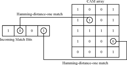
Second, to track whether bits in a CAM array are ACE or un-ACE, this chapter explains how to augment the lifetime analysis of CAM arrays with a technique called hamming-distance-one analysis. The power of ACE analysis to compute AVF arises from its ability to compute the vulnerability of a program from a fault-free execution of the program itself. CAMs, however, make such ACE analysis difficult. A CAM array typically consists of a set of set-associative entries (Figure 4.1). On a CAM match with a set of incoming bits, the corresponding RAM entry is read. ACE analysis with CAMs is difficult because a bit flip in the CAM array can cause an incorrect match against the incoming bits (causing a false-positive match) or a no match when it should have matched (causing a false-negative match). Superficially, it may appear that it will almost be impossible to characterize whether such a bit flip in a CAM array would be ACE or un-ACE without actually flipping a bit in the CAM array and following the subsequent execution of the program. However, the hamming-distance-one analysis can identify the CAM bit or a set of CAM bits that need to be ACE to produce the correct output from a program. Once these bits are identified, one can perform the same lifetime analysis, as is done for RAM array bits, to compute the AVF of the CAM array.

Third, this chapter discusses how to compute AVFs using SFI. Unlike ACE analysis that computes AVFs using a fault-free execution of a program, SFI introduces a sample of faults (bit flips) into a hardware model—typically a gate-level representation called an RTL model during a program’s execution and observes whether that fault caused a user-visible error. If these bit flips eventually cause a program to produce an incorrect output, then the corresponding state elements are ACE. The difficulty with SFI is that to obtain representative results, one needs to inject faults into a detailed gate-level model, which is significantly slower than a performance model, and carry out a large set of experiments to create a proper statistical representation of the AVF. This allows RTL with SFI simulations to only be run for 1000–10 000 cycles per benchmark, which is often inadequate to decide if these elements are ACE or un-ACE because many microarchitectural and architectural states can live significantly longer than 10 000 cycles. However, SFI into an RTL model can be adequate for latches and flip-flops, whose ACE-ness can often be determined within this window of simulation because the lifetime of data held in these state elements is short (only tens or hundreds of cycles). This chapter discusses the basic principles of SFI and how it can be used to compute AVFs using an RTL model.
4.2 Lifetime Analysis of RAM Arrays
This section explains how to extend the AVF analysis to address-based RAM arrays using lifetime analysis and how the differences in properties of different structures and the granularity of the analysis can affect the AVF. Finally, this section illustrates how to compute DUE AVF for RAM arrays that are protected with an error detection mechanism, such as parity.
4.2.1 Basic Idea of Lifetime Analysis
Computing a bit’s AVF involves identifying the fraction of time it is ACE. As in Chapter 3, one can focus on identifying un-ACE components in a bit’s lifetime since it is typically easier to determine if a bit is un-ACE (as opposed to ACE) in a particular cycle. Subtracting the un-ACE time from total time provides an upper bound on the ACE lifetime of the bit. Lifetime analysis of ACE or un-ACE determination is illustrated using the example in Figure 4.2.

Figure 4.2 shows example activities occurring during the lifetime of a bit in an RAM array, such as in a cache. The bit begins in “idle” state but is eventually filled with appropriate values that could be either ACE or un-ACE. The bit is read and written. Eventually, the state contained in the bit is evicted and refilled. The lifetime of this bit can be divided up into several nonoverlapping components: idle, fill-to-read, read-to-read, read-to-write, write-to-write, write-to-read, read-to-evict, and evict-to-fill. By definition, idle and evict-to-fill are un-ACE since there is no valid state in the bit during those intervals. Read-to-write and write-to-write lifetimes are also un-ACE because a strike on the bit after the read (for read-to-write) or first write (for write-to-write) will not result in an error.
Whether the four other lifetime components—fill-to-read, read-to-read, write-to-read, and read-to-evict—are un-ACE depends on the ACE-ness of the reads and the nature of the architectural structure the bit is a part of. If the read itself in fill-to-read is ACE, then the fill-to-read lifetime is ACE. This can be deduced transitively from the ACE-ness of an instruction. For example, if an instruction reading the register file is ACE, then the read itself is ACE, causing the fill-to-read time to become ACE. However, if the read in fill-to-read is un-ACE (due to an un-ACE read), then one cannot conclude that the fill-to-read time is un-ACE itself until the ACE-ness of the subsequent read is determined. If the first read is un-ACE and the second read is ACE (in the read-to-read lifetime), then both fill-to-read and read-to-read are ACE. However, if both the reads are un-ACE, then one cannot conclude if the fill-to-read and the read-to-read lifetimes are ACE or un-ACE before observing the subsequent write. Once the subsequent write (in read-to-write) is observed, then one can know for sure that the read-to-write lifetime is un-ACE. Then both fill-to-read and read-to-read can be marked as un-ACE.
Finally, whether the read-to-evict is ACE or un-ACE depends on the property of the structure the bit resides in. For example, if the structure is a write-through cache, then the evict operation simply discards the value in the bit. This makes the read-to-evict time un-ACE, independent of the ACE-ness of the read itself. However, in a write-back cache, where the value of a modified bit may be written back to a lower-level cache, the analysis is more complex. To determine whether the read-to-evict is ACE or un-ACE, one has to track the ACE-ness of value through its journey through the computer system until it is overwritten. Often, this interstructure analysis is complicated. Hence, one could conservatively assume that if value in the bit is modified and written back on an evict, then read-to-evict time is ACE. The next subsection further examines how properties of a structure can affect the ACE-ness or un-ACE-ness of a lifetime.
In Figure 4.2, compute the AVF for the given lifetime from the first fill to the next fill. Assume the following lifetimes are ACE: fill-to-read and write-to-read. Rest is un-ACE. Fill-to-read time is 10 cycles. Write-to-read time is 20 cycles. Fill-to-fill time is 200 cycles.
SOLUTION Total ACE time = 10 + 20 = 30 cycles. Total time = 200 cycles. AVF = 30/200 = 15%.
A designer is faced with the proposition of evaluating the AVF of a cache and its output latch. Every time the cache is read, the data from the cache are first written to the output latch from where it is read in the next cycle. The designer argues that since every read—hence every ACE read—from the cache is staged through the output latch, the AVF of the output latch should be an upper bound for the AVF of the cache. Is this correct?
SOLUTION This is incorrect. Figure 4.3 shows the lifetime analysis of a counterexample. Consider a one-bit cache with a corresponding output latch. Consider a lifetime sequence of a Fill, 3 ACE Reads, and an Evict. For every ACE Read in the cache, there is a corresponding Write into the output latch followed by an ACE Read in the next cycle after the Write. The AVF of the one-bit cache for this sequence is 12/14 = 86% since Fill to third ACE Read is 12 cycles and total number of cycles is 14. In contrast, the AVF of the output latch is 3/14 = 21%. The AVF of the output latch in this case is significantly smaller than the AVF of the cache. The reason why the AVF of the output latch cannot approximate the AVF of the cache is that the ACE residency time of bits in the cache is significantly longer than that in the output latch. One can easily construct another example to show that the inverse conclusion—whether the AVF of the output latch is a lower bound of the AVF of the cache—is incorrect as well.

4.2.2 Accounting for Structural Differences in Lifetime Analysis
As explained in the previous subsection, the ACE-ness of a bit in a structure depends both on the ACE-ness of the operation on the structure, such as a read, and on certain properties of the structure itself. This section analyzes how ACE-ness can differ for four microprocessor structures: a write-through data cache, a write-back data cache, a data address translation buffer (commonly known as the TLB for translation lookaside buffer), and a store buffer. These structures are described briefly below. Readers are referred to Hennessy and Patterson [4] for detailed architectural descriptions of these structures.
Although a data cache is typically protected in a processor, it is a useful structure to explain how lifetime analysis works. Besides, as will be seen later (in Computing the DUE AVF, p. 131), designers often try to optimize the implementation of ECC to reduce the performance degradation by trading off error rate against performance. The AVF analysis of caches is useful for such trade-off analysis.
Data Caches
A processor’s closest data cache is a structure that usually sits close to the execution units and holds the processor’s most recently and frequently used data. This allows the execution units to compute faster by obtaining data from faster and smaller data caches than from bigger caches or main memory that can be farther away. This section considers a data cache that a processor accesses on every load to read data and on every store to write data. The stores could, however, be routed to the cache via the store buffer discussed later in this section.
Such a data cache can be either a write-through or a write-back. As the name suggests, a write to a write-through data cache writes the data not only to the data cache in question but also to a lower level of the memory hierarchy, which could be a bigger cache or a main memory. Consequently, a write-through data cache never has modified data. In contrast, a write-back data cache keeps modified data and does not propagate the newly written data to a lower level of the memory hierarchy. This is a performance optimization that works well when enough write bandwidth is not available. Eventually, when a cache block needs to be replaced, the modified data are written back and hence the name write-back cache.
As shown in Figure 4.4, the ACE and un-ACE classifications differ for a write-through and a write-back cache (as well as for a data translation buffer and a store buffer). The column “un-ACE” shows the lifetime components that can be definitely identified as un-ACE. The column “Potentially ACE” shows lifetime components, such as fill-to-read, that are possibly ACE, unless one can show through further analysis that these components are un-ACE. For example, if the read and all subsequent reads before eviction can be shown to be un-ACE, then the fill-to-read component becomes un-ACE. Hence, this column is marked potentially ACE. Finally, the column “Unknown” shows lifetime components that remain unresolved because the simulation ends before the resolution could be achieved. The section Effect of Cooldown in Lifetime Analysis, p. 138, examines how a technique called cooldown can reduce this unknown component.

FIGURE 4.4 Lifetime classification of RAM arrays in four processor structures. The sections Accounting for Structural Differences in Lifetime Analysis, p. 125, and Effect of Cooldown in Lifetime Analysis, p. 138, explain components of the table. End here denotes the end of simulation.
In Figure 4.4, the most striking difference in the lifetimes for a write-through and a write-back cache is the write-to-evict component, which is un-ACE for a write-through cache but could be ACE for a write-back cache. The write-to-evict is un-ACE in a write-through cache because on eviction, the data are thrown away. So an upset on any of those bits would not matter. In contrast, in a write-back cache, modified data generated by a write will be written back to the lower levels of the memory hierarchy on eviction. Consequently, those data will be used and could potentially be ACE.
To track whether write-to-evict and other lifetime components are ACE or not, one needs to track the values through the memory hierarchy and hence perform interstructure ACE analysis. For practical purposes, industrial design teams could assume conservatively that any write-to-evict in a write-back cache is ACE, unless the AVF is too high and calls for a more precise analysis. Figure 4.4 bins the lifetime components into ACE or un-ACE based on this conservative assumption. Some of the ACE components could, however, be categorized as un-ACE with further information from interstructure analysis.
Data Translation Buffer
The data translation buffer is a processor structure that caches virtual-to-physical address translations and associated page protection information from the page table. A page table is a common OS structure maintained in software. It allows a virtual user process to map its address space to the physical address space of the machine, thereby supporting virtual memory. Every load and store instruction performs a CAM operation (Figure 4.1) on the data translation buffer with its virtual address. On a CAM hit, a load or a store obtains the corresponding physical address and the associated protection information.
ACE analysis of the data translation buffer RAM is relatively straightforward, particularly because there are no “writes” to a data translation buffer besides the “fill” that writes an entry when it is brought into the buffer. Fill-to-read and read-to-read are again ACE, by default, unless the corresponding load or store that initiated the read is un-ACE and there is no subsequent ACE read on this entry.
Store Buffer
The store buffer is a staging buffer for stores before the store data are written into a coalescing merge buffer. From the merge buffer, the data are written to the cache. For dynamically scheduled processors, a store buffer is particularly important to ensure memory ordering within a program. Like the data cache, the store buffer is written into by store instructions but read by loads. Unlike the data cache, however, each store creates a new entry in the store buffer. Thus, the store buffer can concurrently hold multiple stores to the same address. Also, the store buffer typically has per-byte mask bits to identify the bytes that have been modified. As soon as a store instruction retires, it becomes a candidate for eviction. When a store is evicted, the pipeline moves it to a coalescing merge buffer from where the data are eventually written into the cache hierarchy. The residency times of entries in the store buffer are much shorter than corresponding ones in the data cache or data translation buffer.
Let us now examine which components are ACE and un-ACE. The evict-to-fill time in a store buffer is un-ACE because there is no valid entry in a store buffer once the entry is evicted. Read-to-fill time may be ACE, unlike in a write-through cache. This is because even if the read in read-to-evict is initiated by an un-ACE load, once the entry is evicted, the corresponding data are written back to the cache and could be potentially ACE.
Further, the store buffer is somewhat unique in that a write to the data bit of one entry can change the ACE status of a data bit in a completely different entry. Consider two stores that write to the same byte of a data address. These stores will occupy different entries in the store buffer. In a single-processor system, the bits representing this byte in the store buffer entry associated with the older store become un-ACE as soon as the younger store in the store buffer retires. This is because any subsequent loads to this address will receive their value from the younger store buffer entry.
4.2.3 Impact of Working Set Size for Lifetime Analysis
Besides the nature of an address-based structure, the working set size of a program resident in such structures can have a significant impact on a structure’s AVF. For example, if in a 128-entry data translation buffer, only one entry is ever used, then the AVF will never exceed 1/128. Similarly, if a structure’s miss rate is very high, then the AVF is likely to be low because part of the ACE lifetime gets converted to un-ACE time. For example, an intervening eviction between a write and a read—arising possibly from reduction in a structure’s size or forced eviction—can convert ACE time to un-ACE, thereby reducing that entry’s contribution to overall AVF (Figure 4.5).

FIGURE 4.5 Evictions can reduce the ACE time of a bit or a structure. (a) The original flow. (b) The reduction in ACE time due to an early eviction.
The AVF is harder to predict, however, if the working set size of the structure is just around the size of the structure itself. If the working set size fits just in the structure, then the AVF could be potentially high. But if the structure’s size is reduced slightly, the AVF could go down significantly because of evictions and turnover experienced by the structure.
Consider two scenarios for a 64-entry RAM structure. In both cases, there is a miss followed by one or more ACE reads, followed by a miss again. Then, the pattern repeats. However, in the first one, the following sequence plays out: a miss-to-last read time is 99 cycles followed by a read-to-miss time of one cycle. In the second one, the following sequence occurs: a miss-to-read is one cycle and read-to-miss is one cycle. Consider the ACE reads. Compute the AVF in the two different scenarios.
SOLUTION In the first case, the AVF = 99/(99 + 1) = 99%. In the second case, the AVF is 1/(1 +1) = 50%. The first case experiences a low miss rate, whereas the second case has a fairly high miss rate.
4.2.4 Granularity of Lifetime Analysis
The granularity at which lifetime information is maintained can have a significant impact on the lifetime analysis of certain structures, such as a cache. This relates to accurate accounting in ACE analysis, unlike the previous two issues that relate to the property of a structure and the working set size of a program. Let us consider a cache to understand this point. A cache data (or RAM) array is divided into cache blocks, whose typical size ranges between 32 and 128 bytes. When a byte in a cache block A is accessed, the entire cache block A is fetched into the cache. However, not all the remaining bytes in the block A will be read or written by the processor. When a new cache block B replaces the cache block A, the remaining bytes in block A become un-ACE. This is reflected as fill-to-evict time (see Figure 4.4), which represents the bytes of the data never used before the line is evicted or used only by the initial access. For a write-through cache, fill-to-evict time could be as high as 45% of its total un-ACE time [3].
The write-back cache also needs special consideration. Consider the following scenario in the data array. Two consecutive bytes A and B in the same cache block are fetched into the data array. If A is only read and B is never read prior to eviction, then the fill-to-evict time for B is un-ACE. In contrast, if A is written into, then the fill-to-evict time for B becomes potentially ACE because the entire block (including B) could now be written back into the next level of the cache hierarchy. Thus, a fault in B could propagate to other levels of the memory hierarchy. To handle a write-back cache, the lifetime breakdown must be modified. Bytes of a modified line that have not themselves been modified are ACE from fill-to-evict, regardless of what may happen to them in the interim. The bytes that have been modified are ACE from last write-to-evict and any from earlier write-to-read time. The bytes of an unmodified line work identically to those of a write-through cache. Hence, two of the un-ACE components of a write-back cache (as shown in Figure 4.4), fill-to-evict and read-to-evict, can be conditionally ACE at certain times. This extra ACE component could potentially be reduced by adding multiple modified bits, each representing a portion of the cache line.
For the data translation buffer, it is sufficient to maintain the ACE and un-ACE components on a per-entry basis. For the store buffer data array, however, it may be necessary to maintain the information on a per-byte basis because of the per-byte masks.
Compute the AVF of a structure in which the average residence time is 100 cycles and 40% of the bytes in a block are never touched once they are brought in. There are on average two ACE reads to the other 60% of the bytes in the block. Average fill-to-read time is 40 cycles and read-to-read time is 30 cycles. Read-to-evict time is un-ACE.
SOLUTION The AVF would be 40% × 0 + 60% × (40 + 30)/100 = 42%.
4.2.5 Computing the DUE AVF
All prior discussions in this section focused on determining the SDC AVF, which assumes no protection for a specific structure. Instead, if these structures had fault detection (e.g., via parity protection) and no recovery mechanism, then the corresponding AVF is called DUE AVF. As described in False DUE AVF, p. 86, Chapter 3, one can derive the DUE AVF by summing the original SDC AVF and the resulting false DUE AVF.
In the structures referred to in this section, false DUE AVF from parity protection arises only for a write-back cache and the store buffer. On detecting a parity error, the write-through cache and the data translation buffer can refetch the corresponding entry from the higher-level cache and page table, respectively. That is, with parity and an appropriate recovery mechanism, the DUE AVF of both a write-through data cache and a data translation can be reduced to zero.
In both the write-back cache and the store buffer RAM false DUE arises from dynamically dead loads. When a dynamically dead load reads an entry in the cache or the store buffer RAM array, it can check for errors by recomputing the parity bit. If there is a mismatch between the existing and the computed parity bit, then the cache or the store buffer will signal an error, resulting in a false DUE event.
Assume a processor has a few architecturally visible scratch registers, which are used only in a special mode. Nevertheless, the processor initializes them to zero every time it boots and the OS saves and restores them on every context switch. What is the SDC AVF of these scratch registers? What would be the DUE AVF if the registers were protected with parity and checked for errors every time they are read?
SOLUTION Since the registers are rarely used, the SDC AVF is probably close to zero. If the registers are protected with parity, then whenever the OS saves them, it will be forced to read the registers and declare an error on a parity check violation. Hence, the DUE AVF for these registers are probably close to 100% (Figure 4.6a). Note, however, if the register is actively read and written, the false DUE AVF goes down, even if the OS saves and restores the registers (Figure 4.6b).

To protect against transient faults, processors often have their caches protected with SECDED ECC, where SECDED is for single-error correction and double-error detection (see Chapter 5 for details on how SECDED ECC works). Although SECDED ECC can correct single-bit errors, it can incur an extra cycle of penalty in a high-frequency processor pipeline. To avoid this extra cycle of penalty, a processor designer decided to use the ECC for in-line fault detection, which will not incur this penalty, but out-of-band error recovery to ensure that errors in the cache are eventually corrected. In-line fault detection ensures that when a load accesses the cache line with a fault, it will always detect the error but will not be able to correct it. A background scrubber wakes up periodically, scans one cache line at a time, and corrects any resident error in the cache using the ECC. This is called out-of-band correction since the scrubber is not in the critical path of a load access. AMD’s OpteronTM processor uses a somewhat similar scheme [2].
Let us consider a 16-kilobyte write-through cache, with each ECC covering 8 bytes of data. Also, assume that load accesses to the cache are uniformly distributed, and each ECC-protected word undergoes the following lifetime sequence: fill, ACE read, ACE read, evict. Assume both fill-to-ACE read and ACE read-to-evict time are negligible. ACE read-to-ACE read time per word on average is 1000 cycles. Assume that the scrubber wakes up every 20 cycles (ignore the absence of free read port in the cache), finds the next cache block (size = 64 bytes), and corrects any existing error in all the eight words in the block. For simplicity, assume that the scrubber typically accesses a word halfway between the two ACE reads. How much will the DUE AVF of the cache reduce from this scrubbing scheme?
SOLUTION In the absence of any scrubbing, a load accessing a faulty word will incur a DUE event. Whenever a scrubbing event occurs between two ACE reads, the ACE time from ACE read-to-scrub is converted to un-ACE, which causes the reduction in the DUE AVF (Figure 4.7). However, the cache itself has 256 cache blocks, so the DUE AVF reduction would be roughly 500 cycles (half of the ACE read-to-ACE read time, as per the example) for every 256 × 20 = 5120 cycles. The total time to sequentially scrub the cache is 5120 cycles. Consequently, the DUE AVF reduction in this specific scenario would be ∼10% (500/5120).

FIGURE 4.7 Effects of scrubbing. (a) Fill-to-read and read-to-read are both ACE. (b) Fill-to-read is ACE, but read-to-scrub is un-ACE due to the intervening scrub. It should be noted that the scrub can happen anywhere between the two ACE Reads, and it will still convert the read-to-scrub time to un-ACE.
Using simulation, Biswas et al. [3] showed that the DUE AVF could be reduced by 42% by scrubbing with a 16-kilobyte cache, a 2-GHz processor, and a scrubbing interval of 40 ns (which was the best scrubbing interval for the OpteronTM processor). This analysis scrubs only on idle cache cycles to minimize any disruption in the processor’s performance. The reduction in DUE AVF from scrubbing, however, is highly dependent on the interaccess time of a word, the size of the cache, and the frequency of scrubbing. Consequently, the advantage of scrubbing must be carefully computed based on these design parameters.
4.3 Lifetime Analysis of CAM Arrays
The lifetime analysis of CAMs has both similarities to and differences from that of RAM arrays. Like RAM arrays, CAMs are common hardware structures used in a silicon chip design. For example, tags in data caches are designed with CAMs. As in Figure 4.2, the lifetime analysis of CAMs also involves monitoring activities on the CAM array and identifying the un-ACE portion of a CAM bit’s lifetime. If the soft error contribution of a CAM array is deemed high from its bit count or its AVF computed via the lifetime analysis, then a designer can choose to add to it a protection mechanism, such as parity, ECC bits (see Chapter 5), or radiation-hardened circuits (see Chapter 2).
Unlike RAM arrays, however, one needs to handle false-positive and false-negative matches in CAM arrays. As discussed before, a CAM, such as the tag store, operates by simultaneously comparing the incoming match bits (e.g., an address) against the contents of each of several memory entries (Figure 4.1). Such a CAM can give rise to two types of mismatches, as shown in Figure 4.8. First, incoming bits can match against a CAM entry in the presence of a fault when it should really have mismatched (the false-positive case). If the RAM entry corresponding to the CAM entry is read, then this will cause the RAM array to deliver incorrect data, potentially causing incorrect execution. Similarly, there is a potential for incorrect execution if the RAM entry is written into.

Alternatively, incoming bits may not match any CAM entry, although they should have really matched (the false-negative case). For a write-through cache or a data translation buffer, this would result in a miss, causing the entry to be refetched without causing incorrect execution. However, for a store buffer that holds modified data, this may cause an error because the incoming load would miss in the store buffer and obtain possibly stale data from the cache. An incoming write to a write-back cache will have a similar problem. A false-negative match would refetch an incorrect block to which the write will deposit its data. Methods to handle these scenarios are discussed in more detail below.
4.3.1 Handling False-Positive Matches in a CAM Array
Figure 4.9 shows an example of the false-positive match. The incoming match bits, 1001, would not have matched against the existing CAM entry, 1000, unless the fourth bit is flipped to 1. One can use a technique called hamming-distance-one analysis to compute the AVF of CAM entries. Two sets of bits are said to be apart by hamming distance of one, if they differ in only one bit position. Thus, 1001 and 1000 are apart by a hamming distance of one (in the third bit position, assuming bit positions are marked from zero to three). Similarly, 0001 and 1000 are apart by a hamming distance of two because they differ in the zero-th and third bit positions.

Assuming a single-bit fault model, an incoming set of bits can cause a false-positive match in the CAM array if and only if there exists an entry in the CAM array that differs from the incoming set of bits in one bit position. In other words, false positives are introduced in the CAM entries that are at a hamming distance one from the incoming set of bits. The example in Figure 4.10 shows that only two of the CAM entries are at a hamming distance of one from the incoming bits.
Once the bits that may cause a mismatch have been identified, one can perform the lifetime analysis on these bits. However, because the false-positive case is caused by one particular bit in a tag entry, the ACE analysis of the tag array must be done on a per-bit basis, rather than on a per-entry or a per-byte basis as in the RAM arrays. That is, when a match is found, the bit is marked as potentially ACE. All other bits in the same entry remain un-ACE.
Compute the AVF of a write-through CAM array with 10 4-bit-wide entries over 10 cycles. Assume that only false-positive matches (not false-negative ones) contribute to the AVF. In each cycle, there is an incoming address CAM-ing against the CAM array. During these 10 cycles (marked 0 through 9), there is only one hamming-distance-one match in bit position 1 of entry 1 in cycle 7. Entry 1 gets evicted in cycle 9.
SOLUTION Because the CAM array is write-through, the structure does not hold modified data in the corresponding RAM array. Bit 1 of entry 1 is potentially ACE for eight cycles (cycles 0 through 7) because any fault in bit position 1 between cycles 0 and 7 would deliver a false-positive match in cycle 7. The rest of the bits are un-ACE throughout. The AVF of bit 1 of entry 1 is 8/10 = 80%. The AVF of the rest of the bits throughout these 10 cycles is zero. So the average AVF of the CAM entry is (80% × 1 + 0 × 39)/40 = 2%.
4.3.2 Handling False-Negative Matches in a CAM Array
The false-negative case is easier to track than the false-positive case. The false-negative case occurs when the incoming match bits do not find a match when they should have really matched the bits in a CAM entry. A single-bit fault in any bit of the CAM entry would force a mismatch. On a false-negative match, therefore, all bits in the CAM entry are marked either ACE or un-ACE depending on whether a false miss in the structure would cause incorrect execution. In a data translation buffer or a write-through cache, such a false miss will not cause an incorrect execution, but this would cause an incorrect execution in a write-back cache or a store buffer. In the write-back cache, a false miss could fetch stale data, causing incorrect execution. In the store buffer, an incoming load address CAM-ing against the store buffer will miss and obtain stale data from the data cache, potentially causing incorrect execution.
Interestingly, there is a subtle difference between the RAM and CAM analyses. On a single-bit fault in the RAM array, the actual execution does not necessarily change because the effect of the single-bit fault is localized. In contrast, on a false-negative match in the CAM array, one may not get an actual fault (e.g., as in the write-through cache or the data translation buffer). But the fault can alter the flow of execution because the hardware would potentially bring in a new entry in the CAM array. Biswas et al. [3], however, verified that this effect did not alter the AVF of a microprocessor data translation buffer in any significant way.
4.4 Effect of Cooldown in Lifetime Analysis
As should be apparent by now, properties of structures (e.g., write-back vs. write-through) and time of occurrence of events, such as write, read, or evictions, may have a significant impact on the AVF of a structure. In a similar way, when the AVF simulation ends can also have a significant impact on the AVF of structures. This is termed as an “edge effect.”
The edge effects arise as an artifact of not running a benchmark to completion in a performance model. For example, in Figure 4.11a, if the simulation ended after the fill, then one would not know if the fill-to-end time is ACE or un-ACE and therefore must be marked as unknown. If there were an ACE read after the simulation ended, the fill-to-end time should really have been ACE. Conversely, if there were an eviction after the simulation ended (Figure 4.11b), then the ACE read-to-end time should have been un-ACE instead of unknown. These can have significant impacts on the AVF numbers because designers may have to conservatively assume that AVF = (ACE time + unknown time)/(total time).

FIGURE 4.11 Edge effect in determining ACE and un-ACE time in a write-through structure. In (a), fill-to-end time is unknown when the simulation ends but should really be ACE. In (b), ACE read-to-end time is unknown when the simulation ends but should really be un-ACE.
To tackle these edge effects, Biswas et al. [3] introduced the concept of cooldown, which is complementary to the concept of warm-up in a performance model. A processor model faces a problem at start-up in that initially all processor states, such as the content of the cache, are uninitialized. If simulation begins immediately, the simulator will show an artificially high number of cache misses. This problem can be solved by warming up the caches before activating full simulation. In the warm-up period, no statistics are gathered, but the caches and other structures are warmed up to reflect the steady-state behavior of a processor.
Cooldown is the dual of warm-up and follows the actual statistics-gathering phase in a simulation. During the cooldown interval, one only needs to track events that determine if specific lifetime components, such as fill-to-end or read-to-end, should be ACE or un-ACE. If after the end of the cooldown interval, one cannot precisely determine if the specific lifetime components are ACE or un-ACE, they can be marked as unknown (Figure 4.4).
Figure 4.12 shows the effect cooldown has in reducing the unknown component. The y-axis of the graph shows the average AVF for each structure over all benchmarks. There are two bars associated with each structure. The first bar represents the structure’s AVF without cooldown, and the second represents the AVF with cooldown. The gray section of each bar represents the fraction of AVF that is unknown at simulation end. For every structure other than the tags (CAM) of the data translation buffer, the cooldown period reduces the unknown component by over 50%. Less effect is seen in the data translation buffer because an unknown entry can only be classified after it is evicted, and the data translation buffer has a much lower turnover rate than the other structures. Increasing the cooldown period, however, progressively reduces the unknown component without raising the ACE component, suggesting that asymptotically the unknown component may become negligible.
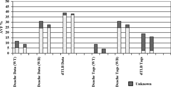
FIGURE 4.12 Effect of cooldown with a 10-million instruction cooldown interval. For each structure, there are two bars. The first bar shows the AVF without cooldown. Reprinted with permission from Biswas et al. [3]. Copyright © 2005 IEEE.
4.5 AVF Results for Cache, Data Translation Buffer, and Store Buffer
This section discusses AVF results for a write-through and a write-back cache, a data translation buffer, and a store buffer. These structures and their differences have been described earlier in this chapter (see Accounting for Structural Differences in Lifetime Analysis, p. 125). The evaluation methodology, performance simulator, and benchmark slices are same as described in Evaluation Methodology, p. 107, Chapter 3. Both the data caches studied are 16-kilobyte four-way set associative. The data translation buffer is fully set associative with 128 entries. The store buffer has 32 entries. All simulations were run for 10 million instructions followed by a cooldown of 10 million instructions. Further details of these experiments are described in Biswas et al. [3].
As per the ACE methodology, the AVF can be divided into two components: potentially ACE and unknown components (Figure 4.4). Potentially ACE components are those that are possibly ACE unless later analysis proves they are un-ACE. Unknown lifetime components are those that are unknown because the simulation ended before resolving whether the components are unknown. As it was seen in Effect of Cooldown in Lifetime Analysis, p. 138, typically these unknown components can be reduced significantly using cooldown techniques. Based on this observation, one can use two AVF terms: upper-bound AVF and best-estimate AVF. Upper-bound AVF includes both potentially ACE and unknown components. In contrast, best-estimate AVF includes only potentially ACE components under the assumption that if one ran the programs to completion, the unknowns would resolve and become mostly un-ACE.
4.5.1 Unknown Components
From the graphs in Figures 4.13–4.16, it is seen that the RAM arrays have an average unknown component of 3% and data cache and store buffer CAM arrays have an average of 4%. The data translation buffer CAM array has a significantly higher unknown component of 13%. This is because the data translation buffer has a significantly lower turnover rate than the data cache. That is, entries tend to stick around in the data translation buffer for long durations—even beyond the simulation and cooldown periods. Thus, all the CAM bits in an entry that do not hamming-distance-one match with a memory operation remain in the unknown state until that entry is evicted from the translation buffer.


Fortunately, hamming-distance-one matches are rare, and each match only adds ACE time to a single bit of the matched tag in the CAM array. Further, separate experiments done by Biswas et al. (not shown here) show that nearly all these bits will eventually resolve to the un-ACE state. Similarly, the unknown lifetime components for the data arrays also resolve mostly to un-ACE if the cooldown period is extended further. Hence, the rest of this section primarily discusses the best-estimate AVF numbers.
4.5.2 RAM Arrays
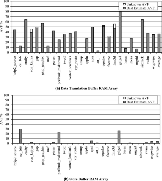
The best estimate of SDC AVFs varies widely across the RAM arrays: from 4% for the store buffer (Figure 4.14) to 6% for the write-through data cache (Figure 4.13) to 25% for the write-back cache (Figure 4.13) to 36% for the data translation buffer (Figure 4.14). If unknown time is included, these rise to 4%, 9%, 28%, and 38%, respectively.
The store buffer’s low SDC AVF arises from its bursty behavior and lower average utilization in most benchmarks. Additionally, the store buffer has per-byte mask bits that identify which of the 16 bytes of an entry is written. Entries that are not written remain un-ACE and do not contribute to the AVF. In the average in-use store buffer entry, only 6 out of the 16 bytes were written.
The data translation buffer’s RAM array has an SDC AVF of 36%, the highest among the RAM arrays discussed in this chapter. This is due to its read-only status and relatively low turnover rate.
The write-through cache’s SDC AVF is relatively low for three reasons. First, on average, over 45% of the bytes read into the cache are accessed only on that initial access or not at all. A read or write to a specific byte or word brings in a whole cache block full of bytes, but many of these other bytes are never accessed. Second, read-to-evict constitutes a significant fraction of the average overall lifetime (over 20%). These results agree with observations made by others (e.g., Lai et al. [6], Wood et al. [10]). Read-to-evict is un-ACE for a write-through cache. It is also un-ACE for a write-back cache, assuming that no write preceded the read. Last, unlike the data translation buffer, a data cache line is modified by stores, indicating that any bytes overwritten by a store are un-ACE in the time period from the last useful read until the write. On the graph, this component of un-ACE time accounts for a little less than 5% of the overall lifetime.
The write-back cache’s SDC AVF is 25% compared to 6% of the write-through cache. This is because a write to a byte of a cache line makes all unmodified bytes in the cache line ACE from the time of the initial fill until the eviction of the line. This is true regardless of the intervening access pattern to that line. Per-byte mask bits (as in the store buffer) would help avoid the write-backs of bytes never modified, thereby reducing the write-back cache’s AVF.
It should be noted that there is a wide variation among the AVFs across benchmarks. Further, AVFs of the different structures for the same benchmark are not necessarily correlated, that is, a high AVF on one structure may not necessarily imply a high AVF on a different structure for the same benchmark. This is true for both the RAM and CAM arrays.
4.5.3 CAM Arrays
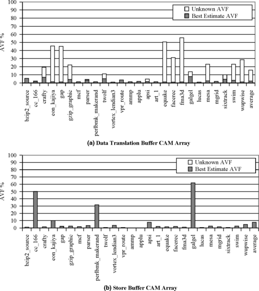
The best-estimate SDC AVFs of the CAM arrays of the write-through cache and the data translation buffer, which do not include unknown time, are quite low: 0.41% and 3%, respectively. These values are considerably lower than the same values for the corresponding data arrays: 6% and 36%, respectively. The low AVF in these CAM arrays arises because the false-negative case—mismatch when there should have been a match—forces a miss and refetch in these structures but does not cause an error. In contrast, the false-positive case—match when there should have been a mismatch—causes an error, but it only affects the ACE state of the single bit that causes the difference. Consequently, there are significantly fewer ACE bits on average in the tag arrays of these structures compared to the data arrays. The write-through tag AVF is particularly low because a hamming-distance-one match would have to occur between the four members of a set to contribute to ACE time.
When including unknown time, SDC AVFs of the CAM arrays of the write-through cache and data translation buffer increase to 4.3% and 16%, respectively. The lower numbers are more representative of the actual AVFs of these two structures because hamming-distance-one matches are so rare, and each hamming-distance-one match makes only 1-bit ACE. If the higher numbers were used, one would be classifying all bits of the tag as ACE at the end point of the simulation. Also, it is likely that these structures would be effectively flushed by a context switch before the end of the cooldown phase (unless the structures have per-process identifiers).
In contrast, the SDC AVF of the store buffer is 7.7%, which is, as per our expectation, higher than that of the corresponding RAM arrays. This is because the store buffer tags are always ACE from fill to evict. The only contributor to un-ACE time for the store buffer tags is the idle lifetime component. The low AVF implies that the store buffer utilization is on average quite low. The CAM AVF is higher than the RAM AVF for the store buffer because all the bytes in the store buffer entry are not written by each store. On average, an in-use store buffer entry contains only 6 valid bytes out of 16 total bytes. Only the valid bytes contribute ACE time.
The SDC AVF of the CAM array of the write-back cache is 25% but is not directly correlated with that of its RAM array. This is because two of the un-ACE components for a write-through cache—fill-to-evict and read-to-evict—may become potentially ACE in a write-back cache. A write-back cache’s CAM entry is always ACE from the time of first modification of its corresponding RAM entry until that entry is evicted.
4.5.4 DUE AVF
A DUE occurs when a fault in a structure can be detected but cannot be recovered from it. Putting parity on the RAM arrays of a write-back cache or a store buffer allows one to detect a fault in a dirty block but not recover from it. To compute the DUE AVF, one can sum the original SDC AVF (same as the true DUE AVF with parity) and false DUE AVF arising from dynamically dead loads. Analysis shows that the false DUE AVF is, on average, an additional 0.2% and 0.5% arising out of dynamically dead loads and stores. Hence, the total DUE AVF for the RAM arrays of a store buffer and write-back cache is 4.2% and 25.5%, respectively. It should be noted that the false DUE AVF component for these structures is significantly less than what was found for an instruction queue (Figure 3.11).
The DUE AVF of the CAM arrays of both a write-back cache and a store buffer is the same as their corresponding SDC AVF (in the absence of parity) since the CAM bits are required to be (conservatively) correct even if the store is dynamically dead. An incorrect CAM entry could result in data being written to a random memory location when the entry is evicted.
Putting parity on a RAM or CAM array of a write-through cache or a data translation buffer allows one to recover from a parity error by refetching the corresponding entry from the higher-level cache or page table, respectively. Consequently, DUE AVF of these arrays can be reduced to zero in the presence of parity.
4.6 Computing AVFs Using SFI into an RTL Model
This chapter so far has discussed how to compute the AVF of RAM and CAM arrays using ACE analysis of fault-free execution. This section discusses how to compute the AVF and assess the relative vulnerabilities of different structures using SFI. First, the equivalence of fault injection and ACE analyses, as well as their advantages and disadvantages, is discussed. Then, two key aspects of the SFI methodology are described. Finally, a case study on SFI done at the University of Illinois at Urbana–Champaign is discussed.
4.6.1 Comparison of Fault Injection and ACE Analyses
Figure 4.17 shows how ACE analysis and SFI can compute the same AVF. Figure 4.17a shows a sequence of operations: a Fill, an ACE Read, an ACE Read, an un-ACE Read, and an Evict. Let us assume that the ACE time is from the Fill to the second ACE Read and the un-ACE time is from the second ACE Read till Evict. Hence, the AVF = ACE Time/(Fill to Evict Time) = 6/15 = 40%.
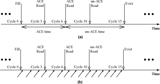
FIGURE 4.17 (a) ACE analysis of an example lifetime. (b) Analysis using fault injection in the same lifetime period. The arrows with the solid head show the injection of a fault into a bit.
Figure 4.17b shows how the same can be achieved via fault injection. In this experiment, the same program is executed 15 times (instead of once as done in ACE analysis). In each of the executions, a fault is injected into a different cycle. For example, during the first execution, the fault is injected into cycle 0; during the second execution, the fault is injected into cycle 1 etc. When a fault is injected, the bit’s value is flipped. That is, it changes to one if it were zero and zero if it were one. The bit’s AVF in this case is defined as the number of errors divided by the number of faults injected. A fault results in an error only when the bit is ACE. Hence, the AVF = 6/15 = 40%. In other words, both fault injection and ACE analyses will ideally yield the same AVF for a bit.
In reality, however, both ACE analysis and fault injection suffer from a number of shortcomings, which limit the scope of their use. ACE analysis relies on precise identification of ACE and un-ACE components of a bit’s lifetime and hence requires executing the program through tens of millions of instructions as well as by using cooldown. Typically, in a microprocessor, a performance model is able to run such a huge number of instructions; hence, ACE analysis is reasonable to apply in a performance simulator. However, a performance simulator does not capture all the detailed microarchitectural state of a machine. For example, typically latches are not present in a performance simulator. Hence, it is difficult to compute the AVF of latches in a performance simulator.
Also, ACE analysis may not be able to track bit flips that cause a control-flow change but do not change the final output of the program (see ACE Analysis Approximates Program Behavior in the Presence of Faults, p. 105). Fault injection can, however, compute the AVF of latches and track control-flow changes and consequent masking because it simulates the propagation of the injected fault through the program execution. Nonetheless, this may not have a large impact on the AVF numbers. For example, using microbenchmarks, Biswas et al. [3] found that both SFI into an RTL model and ACE analysis in a performance model of a commercial-grade microprocessor (built by Intel Corporation) yielded a very similar AVF of the Data Translation Buffer (DTB) CAM and RAM.
Fault injection requires executing a program repeatedly for each injected fault to see if the injected fault results in a user-visible error for the specific instance of the fault. An exhaustive search of this space is almost impossible because it requires an explosive number of experiments spanning the total state of a silicon chip (e.g., upward of 200 million bits in a current microprocessor), potential space of benchmarks running on the chip, and the cycles in which faults can be injected. Instead, practitioners use statistical sampling, which is covered in the next subsection. Because of the statistical nature of this methodology, it is called statistical fault injection.
SFI into a performance simulator may be less meaningful because a performance simulator does not precisely capture the logic state of a silicon chip. Instead, SFI is typically done into a chip’s RTL model consisting primarily of logic gates. Although an RTL model exposes the detailed operation of a processor, it also makes the SFI simulations orders of magnitude slower than those of a performance simulator. This is because large number of simulations must be run to evaluate the AVF of each structure and because the RTL model is itself slow. Consequently, such simulations are often run for 1000–10 000 simulated processor cycles, which is often insufficient to determine if a bit flip is ACE or un-ACE. Hence, SFI may result in large unknowns and hence a conservative estimate of AVF because of lack of knowledge about the ACE-ness of a latch or a bit.
Further, because an RTL model cannot run a program to completion, SFI typically runs two copies of the same program on two RTL models: one faulty and one clean (with no fault). For each fault injection experiment, a fault is injected into one of the RTL models denoted as the faulty model. The clean copy runs the original program without any injected fault. After several cycles—typically, 1000—10 000 cycles—the architectural states of the two models are compared. If the architectural states do not match, then it is often assumed that there is an error and the state in to which the fault was injected is assumed to be ACE. This is, however, not strictly correct since the mismatch could have resulted from the fault injected into an un-ACE state. For example, if the fault was injected into a dynamically dead state, which is un-ACE, the architectural states of the two copies can mismatch, but this may produce no error in the final outcome of the program. This issue is discussed in greater detail later in this chapter.
Finally, an RTL model is often not available during the early design exploration of a processor or a silicon chip, which makes it hard to compute AVFs using SFI. However, performance models are typically created early in the design cycle of a high-performance microprocessor (but not necessarily for chipsets). This leaves the designer with two options to compute AVFs: ACE analysis in a performance model or SFI into an RTL model for an earlier generation of the processor or the silicon chip, if available.
4.6.2 Random Sampling in SFI
To determine a structure’s AVF using fault injection, one can use the following algorithm: pick a bit in the structure, pick a benchmark, and pick a cycle among the total number of cycles the benchmark will run. Start the benchmark execution, and at the predetermined cycle, flip the state of the bit. Then continue running the program until one can determine if the bit flip results in a user-visible error (i.e., bit was ACE at the point of fault injection) or not. Repeat this procedure for the selected list of benchmarks, for every cycle the benchmark executes, and for every bit or state element in the silicon chip. As the reader can easily guess, this results in an explosive number of experiments. For example, with 30 benchmarks, each running a billion cycles, and 200 million state elements, one ends up with 6 × 10¹⁸ experiments. If each experiment took 10 hours to run and one had a thousand computers at one’s disposal to do the experiments, this would still take about 7 × 10¹² years to complete all the experiments. Clearly, this is infeasible.
To reduce this space of experiments, one can randomly select a set of benchmarks, a set of cycles to inject faults into, and a set of bits in each structure. If the random samples are selected appropriately, the computed AVF should asymptotically approach that of the full fault injection or ACE analysis. It should be noted that each fault injection represents a Bernoulli trial with the bit’s AVF as the probability that the specific experiment will cause an error. Then, the minimum number of experiments necessary or n can be computed as
where zα/2 denotes the value of the standard normal variable for the confidence level 100 × (1 – α)% and w is the width of the confidence interval at the particular confidence level [1]. In a layman’s terms, an experimental result that yields an X% confidence interval at a Y% confidence level indicates that if the experiment was repeated 100 times, then on average, Y of the experiments would return a result within X% of the true value of the random variable. The values of z can be obtained from statistical tables (e.g., table 5 in Appendix A in Allen [1]). The AVF is the sample AVF computed as the ratio of user-visible errors and the number of fault injection experiments.
Compute the minimum number of experiments necessary for an AVF of 30% for a 95% confidence level with a 10% error in the AVF in either direction. Repeat the calculation for a 99% confidence level.
SOLUTION For the 95% confidence level, zα/2 = 1.96. For 10% error in the AVF in either direction, w = 2 × 0.1 × 0.3 = 0.06. Hence, n = 4 × 1.962 × 0.3(1 – 0.3)/0.062 = 896.37. So the minimum of fault injection experiments necessary is 897. For the 99% confidence level, zα/2 = 2.576, so n = 4 × 2.5762 × 0.3(1 – 0.3)/0.062 = 1548.35. Hence, the minimum number of fault injections necessary is 1549.
Figure 4.18 shows that the number of experiments required increases with the increase in confidence level and decrease in the error bound. For example, with a 10% error margin in one direction, the number of experiments required increases 4-fold when the confidence level is raised from 90% to 99.9%. Similarly, for a confidence level of 90%, the number of experiments increases 25-fold when the error bound in one direction is tightened from 50% to 10%.

FIGURE 4.18 Number of fault injection experiments necessary to achieve the appropriate confidence level (CL) and error margin (or width) for a sample AVF of 30%. The zα/2 values for 99.9%, 99%, 95%, and 90% CL are 3.291, 2.576, 1.96, and 1.645, respectively. Using these values, the same graph can be reconstructed for different values of AVF.
4.6.3 Determining if an Injected Fault Will Result in an Error
One of the key questions in SFI into an RTL model is to determine if an injected fault actually will result in an error. In ACE terminology, one needs to determine if the bit or the state element is ACE when the fault is injected. Because of the thousands of simulations that must be run for each AVF evaluation for each structure and because the RTL model is usually orders of magnitude slower than a performance simulator, each SFI experiment is typically run for a small number of cycles—typically between 1000 and 10 000 cycles. Determining ACE-ness in this short interval is often a challenge.
SFI will typically run two copies of the RTL simulation: one with a fault and one without a fault (called the clean copy). At the end of the simulation, the faulty model is compared with the clean copy to determine if the injected fault resulted in an error. There are two choices for state to compare: architectural state and microarchitectural state. Architectural state includes register files and memory, and microarchitectural state represents internal state that has not yet been exposed outside the processor (e.g., instruction queue state).
If there is a mismatch in an architectural state between the faulty and the clean copies, then the fault could be potentially ACE. However, just because architectural state is incorrect, it does not necessarily mean that the final outcome of the program will be altered. For example, a faulty value could propagate to an architectural register but later could be overwritten without any intervening reads. That is, the faulty value is dynamically dead. In such an instance, the fault is actually un-ACE and gets masked. Hence, the mismatch in the architectural state only provides a conservative estimate about whether the injected fault is ACE or not.
In contrast, a mismatch in the microarchitectural state, but no mismatch in architectural state, indicates that the fault is latent and may result in an error later in the program after the simulation ends. This is often labeled as unknown since the ACE-ness cannot be determined when the simulation ends. However, if there is no mismatch in either architectural or microarchitectural state, then the fault is masked and therefore is un-ACE.
Many microarchitectural structures, such as a data translation buffer or a cache, can have latent faults long after the simulation ends. This makes it difficult to compute the AVF of such structures using SFI due to the short simulation interval. However, faults in flow-through latches that only contain transient data in the pipeline and affect architectural state can fairly quickly show up as errors in the architectural state if the injected fault is ACE. Hence, computing the AVF of latches using SFI into an RTL model is well suited.
To reduce the simulation time for each fault, the state comparison between the faulty and clean copies is often done periodically, instead of at the end. This is because if the fault is masked completely from both the architectural and the microarchitectural states, then the simulation can end earlier than the predesignated number of cycles the simulation was supposed to run for. Since significant fraction of faults is masked, this could significantly improve simulation time.
4.7 Case Study of SFI
This section will describe the Illinois SFI study conducted by Wang et al. [9]. The Illinois SFI study not only investigates the absolute vulnerability of various processor structures but also delves into the relative vulnerabilities of different structures and latches used in their processor core. For further studies of SFI into an RTL model, readers are referred to Kim and Somani’s work on SFI into a picoJavaTM core [5] and study of SFI into the RTL model of an Itanium® processor by Nguyen, et al. [7].
4.7.1 The Illinois SFI Study
The Illinois SFI study shows the masking effects of injected faults in a dynamically scheduled superscalar processor using a subset of the Alpha ISA. For this study, the authors wrote the RTL model in Verilog from scratch. The authors’ goal was to have a latch-accurate model to study the masking effects from injected faults both in latches as well as in microarchitectural structures.
Processor Model
The processor model used in the Illinois SFI study is a dynamically scheduled superscalar pipeline. Figure 4.19a shows a diagram of this pipeline. Figure 4.19b shows the key processor parameters. To understand the details of this pipeline, the readers are referred to Hennessy and Patterson’s book on computer architecture design [4]. This processor model uses the Alpha ISA but does not execute floating-point instructions, synchronizing memory operations, and a few miscellaneous instructions. The processor resembles a modern, dynamically scheduled superscalar processor.

FIGURE 4.19 The processor model used in the Illinois SFI study. (a) The pipeline. (b) The key processor parameters. Reprinted with permission from Wang et al. [9]. Copyright © 2004 IEEE.
The processor has a 12-stage pipeline with up to 132 instructions in flight. The 32-entry dynamic scheduler can issue up to six IPCs. To support dynamic scheduling, the pipeline supports a load queue (LDQ), store (store queue), speculative RAT (register allocation table), memory dependence predictor (mem dep pred 0 and mem dep pred 1), and a 64-entry ROB (ReOrder Buffer).
4.7.2 SFI Methodology
The Illinois SFI study divides the fault injection experiments into two varieties: those targeting both RAM arrays and latches and those targeting only latches. Each experiment requires repeatedly injecting faults and determining if the fault would result in a user-visible error. Each such fault injection is called a trial of the experiment. In each trial, the authors injected faults into randomly chosen bits from the 31 000 RAM bits and 14 000 latch bits. To achieve statistical significance, fault injection trials were repeated 25 000–30 000 times for each experiment. Each fault injection trial consisted of running a clean copy and a faulty copy for up to 10 000 cycles. However, for simplicity, instead of injecting faults at any randomly chosen cycle, the authors injected the faults on a set of 250–300 start points in the designated faulty copy.
Each trial was continuously monitored for one of the four outcomes: microarchitectural state match (µArch Match), incorrect program output (SDC-Output), premature termination of the workload (SDC-Termination), and none of the above or unknown (Gray Area). µArch Match occurs when the entire microarchitectural state of the processor model (i.e., every bit of state in the machine) is equivalent to that of the clean copy. If a trial results in a microarchitectural state match with no previous architectural state inconsistencies, then it is safe to declare that the injected fault’s effects have been masked by the microarchitectural layer. These trials are placed in the µArch Match category. Since checking for microarchitectural state matches is relatively expensive requiring a full microarchitectural state comparison between the faulty and clean copies, this study only performed the check periodically, taking advantage of the fact that once a microarchitectural state match occurs, the remainder of the simulation is guaranteed to have a consistent microarchitectural state. The check was performed on an exponential time scale: at 1, 10, 100, 1000, and 10 000 cycles after the injection.
The faulty copy’s architectural state (i.e., program-visible state such as memory, registers, and program counter) is compared with that of the clean copy in every cycle. If the architectural state comparison fails, then the transient fault has corrupted architectural state, and the trial is put in the SDC-Output or SDC-Termination bin. Trials that result in register and memory corruptions are conservatively placed into the SDC-Output category, along with those that result in TLB misses. Trials in the SDC-Termination category are those trials that resulted in pipeline deadlock or resulted in an instruction generating an exception, such as memory alignment errors and arithmetic overflow. Strictly speaking, all errors in the SDC-Termination category are SDCs, unless one can definitely prove that the program terminated before corrupting the data that are visible to the user. For example, if corrupted data are written to a database on disk before the program terminates, then the SDC-Terminated error definitely falls in the SDC bin.
If a trial does not result in a µArch Match, SDC-Output, or SDC-Termination, within the 10 000-cycle simulation limit, the trial is placed into the Gray Area category. Either the fault is latent within the pipeline or it is successfully masked, but the timing of the simulation is thrown off such that a complete microarchitectural state match is never detected. Of those that are latent, some will eventually affect architectural state, while others propagate to portions of the processor where they will never affect correct execution.
4.7.3 Transient Faults in Pipeline State
Figure 4.20 shows the results of fault injection experiments into the pipeline state. Each bar in the graph represents a different benchmark application from the SPEC2000 integer benchmark suite. The data from fault injection into latches and RAMs are labeled with an l + r suffix, while data from injection into only latches are labeled with an l suffix. The different benchmarks represent different workloads on the processor, which affect the masking rate of the microarchitecture. The average results are presented in the rightmost bar in the graph I.
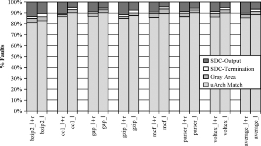
FIGURE 4.20 Results from fault injection into pipeline state. I + r denotes fault injection into both latch and RAM. I denotes fault injection only into latches. Reprinted with permission from Wang et al. [9]. Copyright © 2004 IEEE.
Examining the aggregate bars of both graphs, one can observe that approximately 85% of latch+RAM faults and about 88% of latch-based faults are successfully masked. The fraction of trials in the Gray Area accounts for another 3% for both experiments; the study was not able to determine conclusively whether these faults are masked or not. The remaining 12% of latch+RAM trials and 9% of latch trials are known errors that are either SDC-Output or SDC-Termination.
Figure 4.20 shows the average vulnerability of a latch or a processor state element for different benchmarks. However, previously, it was seen that the AVF of processor structures varies from structure to structure within a benchmark. Figure 4.21 shows a similar variation for latches. This study was done by some of the authors of the Illinois SFI study using the same experimental framework [8].1 In particular, Figure 4.21 shows that 30% of the latches account for 70% of the total soft error contribution from latches. Consequently, these 30% of the latches should be the first target for soft error protection mechanisms.

FIGURE 4.21 Variation in latch vulnerability. Reprinted with permission from Wang and Patel [8]. Copyright © 2006 IEEE.
4.7.4 Transient Faults in Logic Blocks
To understand the vulnerability of logic blocks, each latch or RAM cell in the processor was categorized based on the general function provided by that bit of state. For example, latches and RAM cells that hold instruction input and output operands were placed into a data category. Figure 4.22 lists the various categories of logic blocks used in the Illinois SFI study and provides a brief description for each, as well as the number of bits of latches and RAM cells within that category.

FIGURE 4.22 Description of different categories of state. Reprinted with permission from Wang and Patel [8]. Copyright IEEE © 2006.
The results of the fault injection experiments (for latches and latches+RAMs) were then categorized by the logic block of the bit of state that the fault was injected into and the resulting outcome of the trial. Figure 4.23 shows the results of these experiments categorized by the functional block.
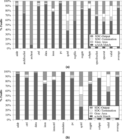
FIGURE 4.23 Results of fault injection into (a) latches and RAM cells and (b) latches alone. Reprinted with permission from Wang and Patel [8]. Copyright © 2006 IEEE.
Figure 4.23a shows that the architectural register alias table (archrat) and the physical register file (regfile) are especially vulnerable to soft errors. This is not surprising since these structures contain the software-visible program state. The speculative register alias table (specrat) and the speculative free list (specfreelist) also appear to be particularly vulnerable. In order to bolster the overall reliability of our microarchitecture, it would be sensible to protect these structures.
Both the latch+RAM injections and the latch-only injections show high vulnerability for the bits categorized as qctrl and valid. Their impact on the overall fail rate is small, however, since they constitute only a small fraction of the total state of the machine. Also, it is interesting to note that the fail rate of the data category is the lowest due to a combination of low utilization rate, speculation, and logical masking.
4.8 Summary
AVF of a hardware structure expresses the fraction of faults that show up as user-visible errors. The intrinsic SER of a structure arising from circuit and device properties must be multiplied by the AVF to obtain the SER of the structure. Both the absolute and relative AVFs are useful. The absolute value of AVF is used to compute the overall chip-level SER. The relative values of AVFs are used to identify structures in need of protection. This chapter extends the AVF analysis described in Chapter 3 to three types of structures: address-based RAM arrays, CAM arrays, and latches.
Computing the AVF of address-based RAM arrays requires an extension called lifetime analysis. Lifetime analysis of a bit or a structure divides up the lifetime of a bit or a structure as a program executes into multiple nonoverlapping segments. For example, for a byte in the cache, the lifetime can be divided into fill-to-read, read-to-read, read-to-write, write-to-read, read-to-evict, etc. Each of these individual lifetime components can be categorized into potentially ACE, un-ACE, or unknown. For example, if the read in fill-to-read is an ACE read (implying the read value affects the final outcome of the executing program), then the fill-to-read component is ACE as well. Similarly, the read-to-evict component could be un-ACE in a write-through cache. Unknown components arise when the analysis cannot determine how the lifetime of a component should be binned (perhaps because the simulation ends prior to the determination of ACE-ness or un-ACE-ness of a component). By summing up all the potentially ACE and unknown lifetime components of a structure and dividing by the total simulation time, one can obtain an upper bound on the structure’s AVF.
The AVF analysis of CAM arrays is slightly more involved. A CAM array, such as a tag store, operates by simultaneously comparing a set of incoming match bits (e.g., an address) against the contents of each of several memory entries. A single-bit fault in the CAM array results in two scenarios that could cause incorrect execution: a false-positive match or a false-negative match. A false-positive match occurs when a bit flip in the CAM array causes a match when there should not have been a match. A false-negative match occurs when a bit flip in the CAM array causes a mismatch when there should have been a match. False-positive matches can be tracked using hamming-distance-one analysis. The incoming match bits and bits of an entry in the CAM array are said to be Hamming distance one apart if they differ in one bit. When a fault occurs, only this bit can give rise to a false-positive match. On encountering a false-positive match and by tracking the lifetime of the bit causing the match, one can compute the AVF arising from such a match. The false-negative match is easier to track. By tracking the lifetime of the CAM entry associated with a false-negative match (i.e., the entry that should have matched), one can compute the corresponding AVF component.
Computing latch AVFs using ACE analysis in a performance model is difficult because a performance model does not typically model the behavior of latches. Instead, it is easier to do in an RTL model that captures the actual behavior of the hardware being built. However, RTL models are usually 100 to 1000 times slower than performance models, making it difficult to run RTL models for more than tens of thousands of cycles to determine AVFs. This is too short for ACE analysis to determine ACE-ness of many structures, and it may be somewhat cumbersome to implement the ACE analysis of a low-level gate-centric RTL model. Instead, it is easier to use SFI to compute the AVF of latches. In SFI, random bit flips simulating faults are introduced in an RTL model to create a faulty copy. Simultaneously, a clean copy is run separately. If after some number of the cycles, the architectural states of the faulty and clean copies differ, then one can assume that the fault is likely to show up as an error. This is not strictly correct but used in practice due to limitations imposed by the RTL model. Such experiments are repeated thousands of times. Each time a different bit may be flipped at a different point in the simulation. By repeating these fault injection experiments, one can obtain a desired level of statistical significance in the AVF numbers.
4.9 Historical Anecdote
I was the lead soft error architect of an Itanium® processor design that was eventually canceled. Itanium® processors are, in general, aggressive about soft error protection. During the design process, we assumed, based on established design guidelines (and not a proper AVF analysis), that the data translation buffer CAM was highly vulnerable to soft errors. Protecting this CAM with parity was difficult because of Itanium architecture’s support of multiple page sizes.
A simple scheme such as adding a parity bit to the CAM and then augmenting the incoming address with the appropriate parity bit to enable the CAM operation did not work. This is because the number of bits of the incoming address over which we needed to compute the parity was determined by the page size, whose information was embedded in the RAM array of the data translation buffer. Thus, we could not compute the parity of the incoming address without looking up the data translation buffer RAM array first.
To tackle this problem, we came up with a novel scheme that simultaneously computed the parity for multiple page sizes and then CAM-ed the data translation buffer appropriately. Details of this scheme are described in the US Patent Application 20060150048 filed to the US patent office on December 30, 2004. This was even coded into the RTL model of the Itanium processor we were building.
Later when we formulated the AVF analysis of address-based structures and computed the AVF of the data translation buffer CAM, we found it to be very small, around 2–3%. This immediately made the soft error contribution of the data translation buffer CAM noncritical to the processor we were building. We would not have protected this CAM, if we had these data prior to making the decision about protecting the CAM array.
References
Allen A.O. Probability, Statistics, and Queue Theory with Computer Science Applications. Academic Press, 1990.
AMD. BIOS and Kernel Developer’s Guide for AMD Athlon™64 and AMD OpteronTM Processors. Publication #26094, Revision 3.14. April 2004. Available at: http://www.amd.com/us-en/assets/content_type/white_papers_and_tech_docs/26094.PDF.
Biswas A., Racunas P., Cheveresan R., Emer J., Mukherjee S.S., Rangan R. Computing Architectural Vulnerability Factors for Address-Based Structures. 32nd Annual International Symposium on Computer Architecture (ISCA). June 2005:532–543.
Hennessy J.L., Patterson D.L. Computer Architecture: A Quantitative Approach. Morgan Kaufmann Publishers, 2003.
Kim S., Somani A.K. Soft Error Sensitivity Characterization for Microprocessor Dependability Enhancement Strategy. International Conference on Dependable Systems and Networks (DSN). June 2002:416–425.
Lai A., Fide C., Falsafi B. Dead-Block Prediction and Dead-Block Correlating Prefetchers. 28th International Symposium on Computer Architecture. June 2001:144–154.
Nguyen H.T., Yagil Y., Seifert N., Reitsma M. Chip-Level Soft Error Estimation Method. IEEE Transactions on Device and Materials Reliability. September 2005;Vol. 5(No. 3):365–381.
Wang N., Patel S.J. ReStore: Symptom-Based Soft Error Detection in Microprocessors. IEEE Transactions on Dependable and Secure Computing. July–September 2006;Vol. 3(No. 3):188–201.
Wang N., Quek J., Rafacz T.M., Patel S.J. Characterizing the Effects of Transient Faults on a High-Performance Processor Pipeline. International Conference on Dependable Systems and Networks (DSN). June 2004:61–70.
Wood D., Hill M., Kessler R. A Model for Estimating Trace-Sample Miss Ratios. 1991 SIGMETRICS Conference on Measurement and Modeling of Computer Systems. May 1991:79–89.
1Although the original paper [8] reports the variation for all processor states, Figure 4.21 shows the variation only for the latches in the design. The authors graciously extracted the latch vulnerability data for this book.