
Introduction
1.1 Overview
In the past few decades, the exponential growth in the number of transistors per chip has brought tremendous progress in the performance and functionality of semiconductor devices and, in particular, microprocessors. In 1965, Intel Corporation’s cofounder, Gordon Moore, predicted that the number of transistors per chip will double every 18–24 months. The first Intel microprocessor with 2200 transistors was developed in 1971, 24 years after the invention of the transistor by John Bardeen, Walter Brattain, and William Shockley in Bell Labs. Thirty-five years later, in 2006, Intel announced its first billion-transistor Itanium® microprocessor—codenamed Montecito—with approximately 1.72 billion transistors. This exponential growth in the number of transistors—popularly known as Moore’s law—has fueled the growth of the semiconductor industry for the past four decades.
Each succeeding technology generation has, however, introduced new obstacles to maintaining this exponential growth rate in the number of transistors per chip. Packing more and more transistors on a chip requires printing ever-smaller features. This led the industry to change lithography—the technology used to print circuits onto computer chips—multiple times. The performance of off-chip dynamic random access memories (DRAM) compared to microprocessors started slowing down resulting in the “memory wall” problem. This led to faster DRAM technologies, as well as to adoption of higher level architectural solutions, such as prefetching and multithreading, which allow a microprocessor to tolerate longer latency memory operations. Recently, the power dissipation of semiconductor chips started reaching astronomical proportions, signaling the arrival of the “power wall.” This caused manufacturers to pay special attention to reducing power dissipation via innovation in process technology as well as in architecture and circuit design. In this series of challenges, transient faults from alpha particles and neutrons are next in line. Some refer to this as the “soft error wall.”
Radiation-induced transient faults arise from energetic particles, such as alpha particles from packaging material and neutrons from the atmosphere, generating electron–hole pairs (directly or indirectly) as they pass through a semiconductor device. Transistor source and diffusion nodes can collect these charges. A sufficient amount of accumulated charge may invert the state of a logic device, such as a latch, static random access memory (SRAM) cell, or gate, thereby introducing a logical fault into the circuit’s operation. Because this type of fault does not reflect a permanent malfunction of the device, it is termed soft or transient.
This book describes architectural techniques to tackle the soft error problem. Computer architecture has long coped with various types of faults, including faults induced by radiation. For example, error correction codes (ECC) are commonly used in memory systems. High-end systems have often used redundant copies of hardware to detect faults and recover from errors. Many of these solutions have, however, been prohibitively expensive and difficult to justify in the mainstream commodity computing market.
The necessity to find cheaper reliability solutions has driven a whole new class of quantitative analysis of soft errors and corresponding solutions that mitigate their effects. This book covers the new methodologies for quantitative analysis of soft errors and novel cost-effective architectural techniques to mitigate them. This book also reevaluates traditional architectural solutions in the context of the new quantitative analysis. To provide readers with a better grasp of the broader problem definition and solution space, this book also delves into the physics of soft errors and reviews current circuit and software mitigation techniques.
Specifically, this chapter provides a general introduction to and necessary background for radiation-induced soft errors, which is the topic of this book. The chapter reviews basic terminologies, such as faults and errors, and dependability models and describes basic types of permanent and transient faults encountered in silicon chips. Readers not interested in a broad overview of permanent faults could skip that section. The chapter will go into the details of the physics of how alpha particles and neutrons cause a transient fault. Finally, this chapter reviews architectural models of soft errors and corresponding trends in soft error rates (SERs).
1.1.1 Evidence of Soft Errors
The first report on soft errors due to alpha particle contamination in computer chips was from Intel Corporation in 1978. Intel was unable to deliver its chips to AT&T, which had contracted to use Intel components to convert its switching system from mechanical relays to integrated circuits. Eventually, Intel’s May and Woods traced the problem to their chip packaging modules. These packaging modules got contaminated with uranium from an old uranium mine located upstream on Colorado’s Green River from the new ceramic factory that made these modules. In their 1979 landmark paper, May and Woods [15] described Intel’s problem with alpha particle contamination. The authors introduced the key concept of Qcrit or “critical charge,” which must be overcome by the accumulated charge generated by the particle strike to introduce the fault into the circuit’s operation. Subsequently, IBM Corporation faced a similar problem of radioactive contamination in its chips from 1986 to 1987. Eventually, IBM traced the problem to a distant chemical plant, which used a radioactive contaminant to clean the bottles that stored an acid required in the chip manufacturing process.
The first report on soft errors due to cosmic radiation in computer chips came in 1984 but remained within IBM Corporation [30]. In 1979, Ziegler and Lanford predicted the occurrence of soft errors due to cosmic radiation at terrestrial sites and aircraft altitudes [29]. Because it was difficult to isolate errors specifically from cosmic radiation, Ziegler and Lanford’s prediction was treated with skepticism. Then, the duo postulated that such errors would increase with altitude, thereby providing a unique signature for soft errors due to cosmic radiation. IBM validated this hypothesis from the data gathered from its computer repair logs. Subsequently, in 1996, Normand reported a number of incidents of cosmic ray strikes by studying error logs of several large computer systems [17].
In 1995, Baumann et al. [4] observed a new kind of soft errors caused by boron-10 isotopes, which were activated by low-energy atmospheric neutrons. This discovery prompted the removal of boro-phospho-silicate glass (BPSG) and boron-10 isotopes from the manufacturing process, thereby solving this specific problem.
Historical data on soft errors in commercial systems are, however, hard to come by. This is partly because it is hard to trace back an error to an alpha or cosmic ray strike and partly because companies are uncomfortable revealing problems with their equipment. Only a few incidents have been reported so far. In 2000, Sun Microsystems observed this phenomenon in their UltraSPARC-II-based servers, where the error protection scheme implemented was insufficient to handle soft errors occurring in the SRAM chips in the systems. In 2004, Cypress semiconductor reported a number of incidents arising due to soft errors [30]. In one incident, a single soft error crashed an interleaved system farm. In another incident, a single soft error brought a billion-dollar automotive factory to halt every month. In 2005, Hewlett-Packard acknowledged that a large installed base of a 2048-CPU server system in Los Alamos National Laboratory—located at about 7000 feet above sea level—crashed frequently because of cosmic ray strikes to its parity-protected cache tag array [16].
1.1.2 Types of Soft Errors
The cost of recovery from a soft error depends on the specific nature of the error arising from the particle strike. Soft errors can either result in a silent data corruption (SDC) or detected unrecoverable error (DUE). Corrupted data that go unnoticed by the user are benign and excluded from the SDC category. But corrupted data that eventually result in a visible error that the user cares about cause an SDC event. In contrast, a DUE event is one in which the computer system detects the soft error and potentially crashes the system but avoids corruption of any data the user cares about. An SDC event can also crash a computer system, besides causing data corruption. However, it is often hard, if not impossible, to trace back where the SDC event originally occurred. Subtleties in these definitions are discussed later in this chapter. Besides SDC and DUE, a third category of benign errors exists. These are corrected errors that may be reported back to the operating system (OS). Because the system recovers from the effect of the errors, these are usually not a cause of concern. Nevertheless, many vendors use the reported rate of correctable errors as an early warning that a system may have an impending hardware problem.
Typically, an SDC event is perceived as significantly more harmful than a DUE event. An SDC event causes loss of data, whereas a DUE event’s damage is limited to unavailability of a system. Nevertheless, there are various categories of machines that guarantee high reliability for SDC, DUE, or both. For example, the classical mainframe systems with triple-modular redundancy (TMR) offer both high degree of data integrity (hence, low SDC) and high availability (hence, low DUE). In contrast, web servers could often offer high availability by failing over to a spare standby system but may not offer high data integrity.
To guarantee a certain level of reliable operation, companies have SDC and DUE budgets for their silicon chips. If you ask a typical customer about how many errors he or she expects in his or her computer system, the response is usually zero. The reality is, though, computer systems do encounter soft errors that result in SDC and DUE events. A computer vendor tries to ensure that the number of SDC and DUE events encountered by its systems is low enough compared to other errors arising from software bugs, manufacturing defects, part wearout, stress-induced errors, etc.
Because the rate of occurrence of other errors differs in different market segments, vendors often have SDC and DUE budgets for different market segments. For example, software in desktop systems is expected to crash more often than that of high-end server systems, where after an initial maturity period, the number of software bugs goes down dramatically [27]. Consequently, the rate of SDC and DUE events needs to be significantly lower in high-end server systems, as opposed to computer systems sitting in homes and on desktops. Additionally, hundreds and thousands of server systems are deployed in a typical data center today. Hence, the rate of occurrence of these events is magnified 100 to 1000 times when viewed as an aggregate. This additional consideration further drives down the SDC and DUE budgets set by a vendor for the server machines.
1.1.3 Cost-Effective Solutions to Mitigate the Impact of Soft Errors
Meeting the SDC and DUE budgets for commercial microprocessor chips, chipsets, and computer memories without sacrificing performance or power has become a daunting task. A typical commercial microprocessor consists of tens of millions of circuit elements, such as SRAM (random access memory) cells; clocked memory elements, such as latches and flip-flops; and logic elements, such as NAND and NOR gates. The mean time to failure (MTTF) of such an individual circuit element could be as high as a billion years. However, with hundreds of millions of these elements on the chip, the overall MTTF of a single microprocessor chip could easily come down to a few years. Further, when individual chips are combined to form a large shared-memory system, the overall MTTF can come down to a few months. In large data centers—using thousands of these systems—the MTTF of the overall cluster can come down to weeks or even days.
Commercial microprocessors typically use several flavors of fault detection and ECC to protect these circuit elements. The die area overheads of these gate- or transistor-level detection and correction techniques could range roughly between 2% to greater than 100%. This extra area devoted to error protection could have otherwise been used to offer higher performance or better functionality. Often, these detection and correction codes would add extra cycles in a microprocessor pipeline and consume extra power, thereby further sacrificing performance. Hence, microprocessor designers judiciously choose the error protection techniques to meet the SDC and DUE budgets without unnecessarily sacrificing die area, performance, or even power.
In contrast, mainframe-class solutions, such as TMR, run identical copies of the same program on three microprocessors to detect and correct any errors. While this approach can dramatically reduce the SDC and DUE, it comes with greater than 200% overhead in die area and a commensurate increase in power. This solution is deemed an overkill in the commercial microprocessor market. In summary, gate-or transistor-level protection, such as fault detection and ECC, can limit the incurred overhead but may not provide adequate error coverage, whereas mainframe-class solutions can certainly provide adequate coverage but at a very high cost (Figure 1.1).

The key to successful design of a highly reliable, yet competitive, microprocessor or chipset is a systematic analysis and modeling of its SER. Then, designers can choose cost-effective protection mechanisms that can help bring down the SER within the prescribed budget. Often this process is iterated several times till designers are happy with the predicted SER. This book describes the current state-of-the-art in soft error modeling, measurement, detection, and correction mechanisms.
This chapter reviews basic definitions of faults, errors, and metrics, and dependability models. Then, it shows how these definitions and metrics apply to both permanent and transient faults. The discussion on permanent faults will place radiation-induced transient faults in a broader context, covering various silicon reliability problems.
1.2 Faults
User-visible errors, such as soft errors, are a manifestation of underlying faults in a computer system. Faults in hardware structures or software modules could arise from defects, imperfections, or interactions with the external environment. Examples of faults include manufacturing defects in a silicon chip, software bugs, or bit flips caused by cosmic ray strikes.
Typically, faults are classified into three broad categories—permanent, intermittent, and transient. The names of the faults reflect their nature. Permanent faults remain for indefinite periods till corrective action is taken. Oxide wearout, which can lead to a transistor malfunction in a silicon chip, is an example of a permanent fault. Intermittent faults appear, disappear, and then reappear and are often early indicators of impending permanent faults. Partial oxide wearout may cause intermittent faults initially. Finally, transient faults are those that appear and disappear. Bit flips or gate malfunction from an alpha particle or a neutron strike is an example of a transient fault and is the subject of this book.
Faults in a computer system can occur directly in a user application, thereby eventually giving rise to a user-visible error. Alternatively, it can appear in any abstraction layer underneath the user application. In a computer system, the abstraction layers can be classified into six broad categories (Figure 1.2)—user application, OS, firmware, architecture, circuits, and process technology. Software bugs are faults arising in applications, OSs, or firmware. Design faults can arise in architecture or circuits. Defects, imperfections, or bit flips from particle strikes are examples of faults in the process technology or the underlying silicon chip.

A fault in a particular layer may not show up as a user-visible error. This is because of two reasons. First, a fault may be masked in an intermediate layer. A defective transistor—perhaps arising from oxide wearout—may affect performance but may not affect correct operation of an architecture. This could happen, for example, if the transistor is part of a branch predictor. Modern architectures typically use a branch predictor to accelerate performance but have the ability to recover from a branch misprediction.
Second, any of the layers may be partially or fully designed to tolerate faults. For example, special circuits—radiation-hardened cells—can detect and recover from faults in transistors. Similarly, each abstraction layer, shown in Figure 1.2, can be designed to tolerate faults arising in lower layers. If a fault is tolerated at a particular layer, then the fault is avoided at the layer above it. The next section discusses how faults are related to errors.
1.3 Errors
Errors are manifestation of faults. Faults are necessary to cause an error, but not all faults show up as errors. Figure 1.3 shows that a fault within a particular scope may not show up as an error outside the scope if the fault is either masked or tolerated. The notion of an error (and units to characterize or measure it) is fundamentally tied to the notion of a scope. When a fault is detected in a specific scope, it becomes an error in that scope. Similarly, when an error is corrected in a given a scope, its effect usually does not propagate outside the scope. This book tries to use the terms fault detection and error correction as consistently as possible. Since an error can propagate and be detected again in a different scope, it is also acceptable to use the term error detection (as opposed to fault detection).
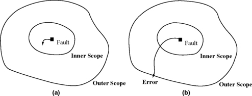
FIGURE 1.3 (a) Fault within the inner scope masked and not visible outside the inner scope. (b) Fault propagated outside the outer scope and visible as an error.
Three examples are considered here. The first one is a fault in a branch predictor. No fault in a branch predictor will cause a user-visible error. Hence, there is no scope outside which a branch predictor fault would show up as an error. In contrast, a fault in a cache cell can potentially lead to a user-visible error. If the cache cell is protected with ECC, then a fault is an error within the scope of the ECC logic. Outside the scope of this logic where our typical observation point would be, the fault gets tolerated and never causes an error. Consider a third scenario in which three complete microprocessors vote on the correct output. If the output of one of the processors is incorrect, then the voting logic assumes that the other two are correct, thereby correcting any internal fault. In this case, the scope is the entire microprocessor. A fault within the microprocessor will never show up outside the voting logic.
In traditional fault-tolerance literature, a third term—failures—is used besides faults and errors. Failure is defined as a system malfunction that causes the system to not meet its correctness, performance, or other guarantees. A failure is, however, simply a special case of an error showing up at a boundary where it becomes visible to the user. This could be an SDC event, such as a change in the bank account, which the user sees. This could also be a detected error (or DUE) caught by the system but not corrected and may lead to temporary unavailability of the system itself. For example, an ATM machine could be unavailable temporarily due to a system reboot caused by a radiation-induced bit flip in the hardware. Alternatively, a disk could be considered to have failed if its performance degrades by 1000x, even if it continues to return correct data.
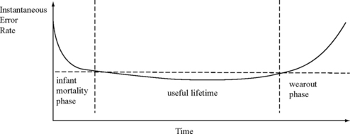
Like faults, errors can be classified as permanent, intermittent, or transient. As the names indicate, a permanent fault causes a permanent or hard error, an intermittent fault causes an intermittent error, and a transient fault causes a transient or soft error. Hard errors can cause both infant mortality and lifetime reliability problems and are typically characterized by the classic bathtub curve, shown in Figure 1.4. Initially, the error rate is typically high because of either bugs in the system or latent hardware defects. Beyond the infant mortality phase, a system typically works properly until the end of its useful lifetime is reached. Then, the wearout accelerates causing significantly higher error rates. The silicon industry typically uses a technique called burn-in to move the starting use point of a chip to the beginning of the useful lifetime period shown in Figure 1.4. Burn-in removes any chips that fail initially, thereby leaving parts that can last through the useful lifetime period. Further, the silicon industry designs technology parameters, such as oxide thickness, to guarantee that most chips last a minimal lifetime period.
1.4 Metrics
Time to failure (TTF) expresses fault and error rates, even though the term TTF refers specifically to failures. As the name suggests, TTF is the time to a fault or an error, as the case may be. For example, if an error occurs after 3 years of operation, then the TTF of that system for that instance is 3 years. Similarly, MTTF expresses the mean time elapsed between two faults or errors. Thus, if a system gets an error every 3 years, then that system’s MTTF is 3 years. Sometimes reliability models use median time to failure (MeTTF), instead of MTTF, such as in Black’s equation for electromigration (EM)–related errors (see Electromigration, p. 15).
Under certain assumptions (e.g., an exponential TTF, see Reliability, p. 12), the MTTF of various components comprising a system can be combined to obtain the MTTF of the whole system. For example, if a system is composed of two components, each with an MTTF of 6 years, then the MTTF of the whole system is


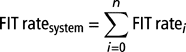
Although the term MTTF is fairly easy to understand, computing the MTTF of a whole system from individual component MTTFs is a little cumbersome, as expressed by the above equations. Hence, engineers often prefer the term failure in time (FIT), which is additive.
One FIT represents an error in a billion (109) hours. Thus, if a system is composed of two components, each having an error rate of 10 FIT, then the system has a total error rate of 20 FIT. The summation assumes that the errors in each component are independent.
The error rate of a component or a system is often referred to as its FIT rate. Thus, the FIT rate equation of a system is
As may be evident by now, FIT rate and MTTF of a component are inversely related under certain conditions (e.g., exponentially distributed TTF):
Thus, an MTTF of 1000 years roughly translates into a FIT rate of 114 FIT.
A silicon chip consists of a billion transistors, each with a FIT rate of 0.00001 FIT. What will be the MTTF of a system composed of 100 such chips?
SOLUTION The FIT rate of each chip = 109 × 0.00001 FIT = 104 FIT. The FIT rate of 100 such chips = 100 × 104 = 106 FIT. Then, the MTTF of a system with 100 such chips = 109/(106 × 24) ∼ 40 days.
What is the MTTF of a computer’s memory system that has 16 gigabytes of memory? Assume FIT per bit is 0.00001 FIT.
SOLUTION The FIT rate of the memory system = 16 × 230 × 8 × 0.00001 = 1 374 390 FIT. This translates into an MTTF of 109/(1 374 390 × 24) ∼ 30 days.
Besides MTTF, two terms—mean time to repair (MTTR) and mean time between failures (MTBF)—are commonly used in the fault-tolerance literature. MTTR represents the mean time needed to repair an error once it is detected. MTBF represents the average time between the occurrences of two errors. As Figure 1.5 shows, MTBF=MTTF + MTTR. Typically, MTTR ![]() MTTF. The next section examines how these terms are used to express various concepts in reliable computing.
MTTF. The next section examines how these terms are used to express various concepts in reliable computing.

Recently, Weaver et al. [26] introduced the term mean instructions to failure (MITF). MITF captures the average number of instructions committed in a microprocessor between two errors. Similarly, Reis et al. [19] introduced the term mean work to failure (MWTF) to capture the average amount of work between two errors. The latter is useful for comparing the reliability for different workloads. Unlike MTTF, both MITF and MWTF try to capture the amount of work done till an error is experienced. Hence, MITF and MWTF are often useful in doing trade-off studies between performance and error rate.
The definitions of MTTF and FIT rate have one subtlety that may not be obvious. Both terms are related to a particular scope (as explained in the last section). Consider a bit with ECC, which can correct an error in the single bit. The MTTF(bit) is significantly lower than the MTTF(bit + ECC). Conversely, the FIT rate(bit) is significantly greater than the FIT rate(bit + ECC). In both cases, it is the MTTF that is affected and not the MTBF. Vendors, however, sometimes incorrectly report MTBF numbers for the components they are selling, if they add error correction to the component.
All the above metrics can be applied separately for SDC or DUE. Thus, one can talk about SDC MTTF or SDC FIT. Similarly, one can express DUE MTTF or DUE FIT. Usually, the total SER is expressed as the sum of SDC FIT and DUE FIT.
1.5 Dependability Models
Reliability and availability are two attributes typically used to characterize the behavior of a system experiencing faults. This section discusses mathematical models to describe these attributes and the foundation behind the metrics discussed in the last section. This section will also discuss other miscellaneous related models used to characterize systems experiencing faults.
1.5.1 Reliability
The reliability R(t) of a system is the probability that the system does not experience a user-visible error in the time interval (0, t]. In other words, R(t)=P(T > t), where T is a random variable denoting the lifetime of a system. If a population of N0 similar systems is considered, then R(t) is the fraction of the systems that survive beyond time t. If Nt is the number of systems that have survived until time t and E(t) is the number of systems that experienced errors in the interval (0, t], then
Differentiating this equation, one gets
The instantaneous error rate or hazard rate h(t)—graphed in Figure 1.4—is defined as the probability that a system experiences an error in the time interval Δt, given that it has survived till time t. Intuitively, h(t) is the probability of an error in the time interval (t, t + Δt].

The general solution to this differential equation is
If one assumes that h(t) has a constant value of λ (e.g., during the useful lifetime phase in Figure 1.4), then
This exponential relationship between reliability and time is known as the exponential failure law, which is commonly used in soft error analysis. The expectation of R(t) is the MTTF and is equal to λ.
The exponential failure law lets one sum FIT rates of individual transistors or bits in a silicon chip. If it is assumed that a chip has n bits, where the ith bit has a constant and independent hazard rate of hi, then, R(t) of the whole chip can be expressed as

Thus, the reliability function of the chip is also exponentially distributed with a constant FIT rate, which is the sum of the FIT rates of individual bits.
The exponential failure law is extremely important for soft error analysis because it allows one to compute the FIT rate of a system by summing the FIT rates of individual components in the system. The exponential failure law requires that the instantaneous SER in a given period of time is constant. This assumption is reasonable for soft error analysis because alpha particles and neutrons introduce faults in random bits in computer chips. However, not all errors follow the exponential failure law (e.g., wearout in Figure 1.4). The Weibull or log-normal distributions could be used in cases that have a time-varying failure rate function [18].
1.5.2 Availability
Availability is the probability that a system is functioning correctly at a particular instant of time. Unlike reliability, which is defined over a time interval, availability is defined at an instant of time. Availability is also commonly expressed as
Thus, availability can be increased either by increasing MTTF or by decreasing MTTR.
Often, the term five 9s or six 9s is used to describe the availability of a system. The term five 9s indicates that a system is available 99.999% of the time, which translates to a downtime of about 5 minutes per year. Similarly, the term six 9s indicates that a system is available 99.9999% of the time, which denotes a system downtime of about 32 seconds per year. In general, n 9s indicate two 9s before the decimal point and (n – 2) 9s after the decimal point, if expressed in percentage.
If the MTTR of a system is 30 minutes, how many crashes can it sustain per year and still maintain a five 9s uptime? What is the MTTF in this case?
SOLUTION A five 9s uptime denotes a total downtime of about 5 hours per year. Hence, the number of system crashes allowed for this system per year is (5 × 60/30) = 10. The MTTF is (1 year–5 hours)/10 = 876 hours.
1.5.3 Miscellaneous Models
Three other models, namely maitainability, safety, and performability, are often used to describe systems experiencing faults. Maintainability is the probability that a failed system will be restored to its original functioning state within a specific period of time. Maintainability can be modeled as an exponential repair law, a concept very similar to the exponential failure law.
Safety is the probability that a system will either function correctly or fail in a “safe” manner that causes no harm to other related systems. Thus, unlike reliability, safety modeling incorporates a “fail-stop” behavior. Fail-stop implies that when a fault occurs, the system stops operating, thereby preventing the effect of the fault to propagate any further.
Finally, performability of a system is the probability that the system will perform at or above some performance level at a specific point of time [10]. Unlike reliability, which relates to correct functionality of all components, performability measures the probability that a subset of functions will be performed correctly. Graceful degradation, which is a system’s ability to perform at a lower level of performance in the face of faults, can be expressed in terms of a performability measure.
These models are added here for completeness and will not be used in the rest of this book. The next few sections discuss how the reliability and availability models apply to both permanent and transient faults.
1.6 Permanent Faults in Complementary Metal Oxide Semiconductor Technology
Dependability models, such as reliability and availability, can characterize both permanent and transient faults. This section examines several types of permanent faults experienced by complementary metal oxide semiconductor (CMOS) transistors. The next section discusses transient fault models for CMOS transistors. This section reviews basic types of permanent faults to give the reader a broad understanding of the current silicon reliability problems, although radiation-induced transient faults are the focus of this book.
Permanent faults in CMOS devices can be classified as either extrinsic or intrinsic faults. Extrinsic faults are caused by manufacturing defects, such as contaminants in silicon devices. Extrinsic faults result in infant mortality, and the fault rate usually decreases over time (Figure 1.4). Typically, a process called burn-in, in which silicon chips are tested at elevated temperatures and voltages, is used to accelerate the manifestation of extrinsic faults. The defect rate is expressed in defective parts per million.
In contrast, intrinsic faults arise from wearout of materials, such as silicon dioxide, used in making CMOS transistors. In Figure 1.4, the intrinsic fault rate corresponds to the wearout phase and typically increases with time. Several architecture researchers are examining how to extend the useful lifetime of a transistor device by delaying the onset of the wearout phase and decreasing the use of the device itself.
This section briefly reviews intrinsic fault models affecting the lifetime reliability of a silicon device. Specifically, this section examines metal and oxide failure modes. These fault models are discussed in greater detail in Segura and Hawkins’ book [23].
1.6.1 Metal Failure Modes
This section discusses the two key metal failure modes, namely EM and metal stress voiding (MSV).
Electromigration
EM is a failure mechanism that causes voids in metal lines or interconnects in semiconductor devices (Figure 1.6). Often, these metal atoms from the voided region create an extruding bulge on the metal line itself.
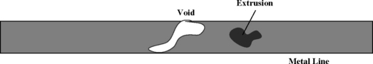
EM is caused by electron flow and exacerbated by rise in temperature. As electrons move through metal lines, they collide with the metal atoms. If these collisions transfer sufficient momentum to the metal atoms, then these atoms may get displaced in the direction of the electron flow. The depleted region becomes the void, and the region accumulating these atoms forms the extrusion.
Black’s law is commonly used to predict the MeTTF of a group of aluminum interconnects. This law was derived empirically. It applies to a group of metal interconnects and cannot be used to predict the TTF of an individual interconnect wire. Black’s law states that
where A0 is a constant dependent on technology, je is electron current density (A/cm2), T is the temperature (K), Ea is the activation energy (eV) for EM failure, and k is the Boltzmann constant. As technology shrinks, the current density usually increases, so designers need to work harder to keep the current density at acceptable levels to prevent excessive EM. Nevertheless, the exponential temperature term has a more acute effect on MeTTF than current density.
Use Black’s equation to estimate relative average lifetimes of two identical parts. A metal line in part 1 runs at 70° C with a maximum current density of 1MA/cm2. A similar metal line in part 2 runs at 100°C with a maximum current density of 2 MA/cm2. Use Ea = 0.8 eV and k = 86.17/μ eV/K.
An additional phenomenon called the Blech effect dictates whether EM will occur. Ilan Blech demonstrated that the product of the maximum metal line length (lmax) below which EM will not occur and the current density je) is a constant for a given technology.
Metal Stress Voiding
MSV causes voids in metal lines due to different thermal expansion rates of metal lines and the passivation material they bond to. This can happen during the fabrication process itself. When deposited metal reaches 400° C or higher for a passivation step, the metal expands and tightly bonds to the passivation material. But when cooled to room temperature, enormous tensile stress appears in the metal due to the differences in the thermal coefficient of expansion of the two materials. If the stress is large enough, then it can pull a line apart. The void can show up immediately or years later.
The MTTF due to MSV is given by
where T is the temperature, T0 is the temperature at which the metal was deposited, B0, n, and Eb are material-dependent constants, and k is the Boltzmann constant. For copper, n = 2.5 and Eb = 0.9. The higher the operating temperature, lower is the term (T0 – T) and higher the MTTFMSV. Interestingly, however, the exponential term drops rapidly with a rise in the operating temperature and usually has the more dominant effect.
In general, copper is more resistive to EM and MSV than aluminum. Copper has replaced aluminum for metal lines in the high-end semiconductor industry. Copper, however, can cause severe contamination in the fab and therefore needs a more carefully controlled process.
1.6.2 Gate Oxide Failure Modes
Gate oxide reliability has become an increasing concern in the design of high-performance silicon chips. Gate oxide consists of thin noncrystalline and amorphous silicon dioxide (SiO2). In a bulk CMOS transistor device (Figure 1.7), the gate oxide electrically isolates the polysilicon gate from the underlying semiconductor crystalline structure known as the substrate or bulk of the device. The substrate can be constructed from either p-type silicon for n-type metal oxide semiconductor (nMOS) transistors or n-type silicon for p-type metal oxide semiconductor (pMOS) transistors. The source and drain are also made from crystalline silicon but implanted with dopants of polarity opposite to that of the substrate. Thus, for example, an nMOS source and drain would be doped with an n-type dopant.

The gate is the control terminal, whereas the source provides electrons or hole carriers that are collected by the drain. When the gate terminal voltage of an nMOS (pMOS) transistor is increased (decreased) sufficiently, the vertical electric field attracts minority carriers (electrons in nMOS and holes in pMOS) toward the gate. The gate oxide insulation stops these carriers causing them to accumulate at the gate oxide interface. This creates the conducting channel between the source and drain, thereby turning on the transistor.
The switching speed of a CMOS transistor—going from off to on or the reverse—is a function of the gate oxide thickness (for a given gate oxide). As transistors shrink in size with every technology generation, the supply voltage is reduced to maintain the overall power consumption of a chip. Supply voltage reduction, in turn, can reduce the switching speed. To increase the switching speed, the gate oxide thickness is correspondingly reduced. Gate oxide thicknesses, for example, have decreased from 750 Å from the 1970s to 15 Å in the 2000s, where 1Å = 1angstrom = 10−10m. SiO2 molecules are 3.5 Å in diameter, so gate oxide thicknesses rapidly approach molecular dimensions. Oxides with such a low thickness—less than 30 Å—are referred to as ultrathin oxides.
Reducing the oxide thickness further has become challenging since the oxide layer runs out of atoms. Further, a thinner gate oxide increases oxide leakage. Hence, the industry is researching into what is known as high-k materials, such as hafnium dioxide (HfO2), zirconium dioxide (ZrO2), and titanium dioxide (TiO2), which have a dielectric constant or “k” above 3.9, the “k” of silicon dioxide. These high-k oxides are thicker than SiO2. Besides, they reduce the oxide leakage when the transistor is off without affecting the transistor’s performance when it is on.
This section discusses three oxide failure mechanisms—wearout in ultrathin oxides, hot carrier injection (HCI), and negative bias temperature instability (NBTI).
Gate Oxide Wearout
Ultrathin oxide breakdown causes a sudden discontinuous increase in conductance, often accompanied by an increased current noise. This causes a reduction in the “on” current of the transistor. Gradual oxide breakdown may initially lead to intermittent faults but may eventually prevent the transistor from functioning correctly, thereby causing a permanent fault in the device.
The breakdown is caused by gradual buildup of electron traps, which are oxide defects produced by missing oxygen atoms. Such electron traps can exist from the point of oxide creation, or they can be created when the SiO2–SiO2 bonds are broken by energetic particles, such as electrons, holes, or radiations. The precise point at which the breakdown occurs is statistically distributed, so only statistical averages can be predicted. The breakdown occurs when a statistical distribution of these traps is vertically aligned and allows a thermally damaging current to flow through the oxide. This is known as the percolation model of wearout and breakdown.
The time-to-breakdown (Tbd) for gate oxide could be expressed as
where C is a constant, tox is the gate oxide thickness, Tj is the average junction temperature, Ea is the activation energy, VG is the gate voltage, and γ and α are technology-dependent constants. Thus, Tbd decreases with decreasing oxide thickness but increases with decreasing VG.
The Tbd model is still an area of active research. Please refer to Strathis [22] for an in-depth discussion of this subject.
Hot Carrier Injection
HCI results in a degradation of the maximum operating frequency of the silicon chip. HCI arises from impact ionization when electrons in the channel strike the silicon atoms around the drain–substrate interface. This could happen from one of several conditions, such as higher power supply, short channel lengths, poor oxide interface, or accidental overvoltage in the power rails.
The ionization produces electron–hole pairs in the drain. Some of these carriers enter the substrate, thereby increasing the substrate current Isub. A small fraction of carriers created from the ionization may have sufficient energy (3.1 eV for electrons and 4.6 eV for holes) to cross the oxide barrier and enter the oxide to cause damage. Because these carriers have a high mean equivalent temperature, they are referred to as “hot” carriers. Interestingly, however, HCI becomes worse as ambient temperature decreases because of a corresponding increase in carrier mobility.
Compute the mean equivalent temperature of an electron with energy of 3.1 eV. Assume that the thermal energy follows the Boltzmann distribution: Et = kT/q, where Et is thermal energy, T is the temperature (K), and k is the Boltzmann constant = 1.38 × 10⁻²³J/K, and q = 1.6 × 10⁻¹⁹ C.
SOLUTION Rearranging the terms of the equation, the mean equivalent temperature T = Etq/k = 3.1 × 1.6 × 10−19/(1.38 × 10−3) ∼ 36 000 K.
Typically, the drain saturation current (IDsat) degradation is used to measure HCI degradation because IDsat is one of the key transistor parameters that most closely approximates the impact on circuit speed and because HCI-related damage occurs only during normal operation when the transistor is in saturation. Oxide damage due to HCI raises the threshold voltage of an nMOS transistor causing IDsat to degrade.
Frequency guardbanding is a typical measure adopted by the silicon chip industry to cope with HCI-related degradation. The expected lifetime of a silicon chip is often between 5 and 15 years. Usually, the frequency degradation during the expected lifetime is between 1% and 10%. Hence, the chips are rated at a few percentage points below what they actually run at. This reduction in the frequency is called the frequency guardband.
Transistor lifetime degradation (τ) due to HCI (e.g., 3% reduction in threshold voltage) is specified as

where W is the transistor width, ID is the drain current, and Isub is the substrate current. The ID and Isub parameters are typically estimated for the use condition of the chip (e.g., power on).
Negative Bias Temperature Instability
Like HCI, NBTI causes degradation of maximum frequency. Unlike HCI, which affects both nMOS and pMOS devices, NBTI only affects short-channel pMOS transistors (hence the term “negative bias”). The “hydrogen-release” model provides the most popular explanation for this effect. Under stress (e.g., high temperature), highly energetic holes bombard the channel–oxide interface, electro-chemically react with the oxide interface, and release hydrogen atoms by breaking the silicon–hydrogen bonds. These free hydrogen atoms combine with oxygen or nitrogen atoms to create positively charged traps at the oxide–channel interface. This causes a reduction in mobility of holes and a shift in the pMOS threshold voltage in the more negative direction. These effects cause the transistor drive current to degrade, thereby slowing down the transistor device. The term “instability” refers to the variation of threshold voltage with time. Researchers are actively looking into models that can predict how NBTI will manifest in future process generations.
1.7 Radiation-Induced Transient Faults in CMOS Transistors
Transient faults in semiconductor devices can be induced by a variety of sources, such as transistor variability, thermal cycling, erratic fluctuations of minimum voltage at which a circuit is functional, and radiation external to the chip. Transistor variability arises due to the random dopant fluctuations, use of subwavelength lithography, and high heat flux across the silicon die [5]. Thermal cycling can be caused by repeated stress from temperature fluctuations. Erratic fluctuations in the minimum voltage of a circuit can be caused by gate oxide soft breakdown in combination with high gate leakage [1].
This book focuses on radiation-induced transient faults. There are two sources of radiation-induced faults—alpha particles from packaging and neutrons from the atmosphere. This section discusses the nature of these particles and how they introduce errors in silicon chips. The permanent faults described earlier in this chapter and the transient faults discussed in the last paragraph can mostly be taken care of before a chip is shipped. In contrast, a radiation-induced transient fault is typically addressed in the field with appropriate fault detection and error correction circuitry.
1.7.1 The Alpha Particle
An alpha particle consists of two protons and two neutrons bound together into a particle that is identical to a helium nucleus. Alpha particles are emitted by radioactive nuclei, such as uranium or radium, in a process known as alpha decay. This sometimes leaves the nucleus in an excited state, with the emission of a gamma ray removing the excess energy.
The alpha particles typically have kinetic energies of a few MeV, which is lower than those of typical neutrons that affect CMOS chips. Nevertheless, alpha particles can affect semiconductor devices because they deposit a dense track of charge and create electron–hole pairs as they pass through the substrate. Details of the interaction of alpha particles and neutrons with semiconductor devices are described below.
Alpha particles can arise from radioactive impurities used in chip packaging, such as in the solder balls or contamination of semiconductor processing materials. It is very difficult to eliminate alpha particles completely from the chip packaging materials. Small amounts of epoxy or nonradioactive lead can, however, significantly reduce a chip’s sensitivity to alpha particles by providing a protective shield against such radiation. Even then, chips are still exposed to very small amounts of alpha radiation. Consequently, chips need fault detection and error correction techniques within the semiconductor chip itself to protect against alpha radiation.
1.7.2 The Neutron
The neutron is one of the subatomic particles that make up an atom. Atoms are considered to be the basic building blocks of matter and consist of three types of subatomic particles: protons, neutrons, and electrons. Protons and neutrons reside inside an atom’s dense center. A proton has a mass of about 1.67 × 10⁻²⁷kg. A neutron is only slightly heavier than a proton. An electron is about 2000 times lighter than both a proton and a neutron. A proton is positively charged, a neutron is neutral, and an electron is negatively charged. An atom consists of an equal number of protons and electrons and hence it is neutral itself.
Figure 1.8 shows the two dominant models of an atom. In the Bohr model (Figure 1.8a), electrons circle around the nucleus at different levels or orbitals much like planets circle the sun. Electrons can exist at definite energy levels, but can move from one energy state to another. Electrons release energy as electromagnetic radiation when they change state. The Bohr model explains the mechanics of the simplest atoms, like hydrogen. Figure 1.8b shows the wave model of an atom in which electrons form a cloud around the nucleus instead of orbiting around the nucleus, as in the Bohr model. This is based on quantum theory. Recently, the string theory has tried explaining the structure of an atom as particles on a string.

The neutrons that cause soft errors in CMOS circuits arise when atoms break apart into protons, electrons, neutrons. The half-life of a neutron is about 10–11 minutes,1 unlike a proton whose half-life is about 1032 years. Thus, protons can persist for long durations before decaying and constitute the majority of the primary cosmic rays that bombard the earth’s outer atmosphere. When these protons and associated particles hit atmospheric atoms, they create a shower of secondary particles, which constitute the secondary cosmic rays. The particles that ultimately hit the earth’s surface are known as terrestrial cosmic rays. The rest of the section describes these different kinds of cosmic rays.
Computers used in space routinely encounter primary and secondary cosmic rays. In contrast, computers at the earth’s surface need only deal with terrestrial cosmic rays, which are easier to protect against compared to primary and secondary cosmic rays. This book focuses on architecture design for soft errors encountered by computers used closer to the earth’s surface (and not in space).
Primary Cosmic Rays
Primary cosmic rays consist of two types of particles: galactic particles and solar particles. Galactic particles are believed to arise from supernova explosions, stellar flares, and other cosmic activities. They consist of about 92% protons, 6% alpha particles, and 2% heavier atomic nuclei. Galactic particles typically have energies above 1 GeV.2 The highest energy recorded so far for a galactic particle is 3 × 10²⁰ eV. As a reference point, the energy of a 1020 eV particle is the same as that of a baseball thrown at 50 miles per hour [7]. These particles have a flux of about 36 000 particles/cm2-hour (compared to about 14 particles/cm2-hour that hit the earth’s surface).
As the name suggests solar particles arise from the sun. Solar particles have significantly less energy than galactic particles. Typically, a particle needs about 1 GeV of energy or more to penetrate the earth’s atmosphere and reach sea level, unless the particle traverses down directly into the earth’s magnetic poles. Whether solar particles have sufficient energy or flux to penetrate the earth’s atmosphere depends on the solar cycle.
The solar cycle—also referred to as the sunspot cycle—has a period of about 11 years. Sunspots are dark regions on the sun with strong magnetic fields. They appear dark because they are a few thousand degrees cooler than their surroundings. Few sunspots appear during the solar minimum when the luminosity of the sun is stable and quite uniform. In contrast, at the peak of the solar cycle, hundreds of sunspots appear on the sun. This is accompanied by sudden, violent, and unpredictable bursts of radiation from solar flares. The last solar maximum was around the years 2000–2001.
Interestingly, the sea-level neutron flux is minimum during the solar maximum and maximum during the solar minimum. During the solar maximum, the number of solar particles does indeed increase by a million-fold and exceeds that of the galactic particles. This large number of solar particles creates an additional magnetic field around the earth. This field increases the shielding against intragalactic cosmic rays. The net effect is that the number of sea-level neutrons decreases by 30% during the solar maximum compared to that during the solar minimum.
Overall, neutrons from galactic particles are still the dominant source of neutrons on the earth’s surface. This conclusion is further supported by the fact that flux of terrestrial cosmic rays varies by less than 2% between day and night.
Both the flux and energy of neutrons determine the SER experienced by CMOS chips. To the first order for a given CMOS circuit, the SER from cosmic rays is proportional to the neutron flux. The energy of these particles also makes a difference, but the relationship is a little more complex and will be explained later in the chapter.
Secondary Cosmic Rays
Secondary cosmic rays are produced in the earth’s atmosphere when primary cosmic rays collide with atmospheric atoms. This interaction produces a cascade of secondary particles, such as pions, muons, neutrons. Pions and muons decay spontaneously because their mean lifetimes are in nanoseconds and microseconds, respectively. Neutrons have a mean lifetime of 10–11 minutes, so they survive longer. But most of these neutrons lose energy and are lost from the cascade. Nevertheless, they collide again with atmospheric atoms and create new showers and further cascades.
The flux of these secondary particles varies with altitude. The flux of secondary particles is relatively small in the outer atmosphere where the atmosphere is not as thick. The flux continues to increase as the altitude drops and peaks at around 15 km (also known as the Pfotzer point). The density of secondary particles continues to decrease thereafter till sea level.
Figure 1.9 shows the variation of neutron flux with altitude. This variation in flux is given by the following equation [30], where H is the altitude in kilometers:
This equation is a rough approximation of how the neutron flux varies with altitude. A more detailed calculation can be found in the joint electron device engineering council (JEDEC) standard [13].3
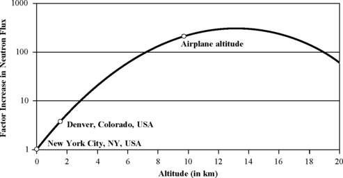
FIGURE 1.9 Variation of neutron flux with altitude. In Denver, Colorado, for example, the neutron flux is about 3.5 times higher than that in New York City, which is at sea level.
Airplanes typically fly at an altitude of 10 km. What is the increase in neutron flux over the sea level at this altitude?
SOLUTION The equation given above shows that the neutron flux increases by 228 times over sea level at an altitude of 10 km at which airplanes typically fly. This implies that the SER of CMOS chips operating in airplanes will be 228 times higher than what the same chips experience at sea level.
Please note that the SER experienced by CMOS chips will be slightly higher than indicated by the neutron flux equation given above. This is because of the presence of other particles, such as pions and muons, besides neutrons.
Terrestrial Cosmic Rays
Terrestrial cosmic rays refer to those cosmic particles that finally hit the earth’s surface. Terrestrial cosmic rays primarily arise from the cosmic ray cascades and consist of fewer than 1% primary particles.
Both the distribution of energy and flux of neutrons determine the SER experienced by CMOS chips. Figure 1.10 shows the distribution of neutron flux with energy based on a recent measurement by Gordon et al. [9]. Typically, only neutrons above 10 MeV affect CMOS chips today.4 To the first order, the SER is proportional to the neutron flux. Integrating the area under the curve in Figure 1.10 gives a total neutron flux of about 14 neutrons per cm2-hour. Earlier measurements by Ziegler in 1996, however, had suggested about 20 neutrons per cm2-hour [28]. The JEDEC standard [13] has agreed to use the recent data of Gordon et al. instead of Ziegler’s, possibly because the more recent measurements are more accurate.

FIGURE 1.10 Terrestrial differential neutron flux (neutrons/cm2-MeV-hour) plotted as a function of the neutron energy. The area under the curve gives a total neutron flux of about 14 neutrons/cm2-Mev-hour.
The neutron flux varies not only with altitude but also with the location on the earth. The earth’s magnetic field can bend both primary and secondary cosmic particles and reflect them back into space. The minimum momentum necessary for a normally incident particle to overcome the earth’s magnetic intensity and reach sea level is called the “geomagnetic rigidity (GR)” of a terrestrial site. The higher the GR of a site, the lower is the terrestrial cosmic ray flux. The GR at New York City is 2 GeV and hence only particles with energies above 2 GeV can cause a terrestrial cascade.
Typically, the magnetic field only causes the neutron flux to vary across any two terrestrial sites by only about a factor of 2x. The GR is highest near the equator (about 17 GeV) and hence the neutron flux is lowest there. In contrast, the GR is lowest near the north and south poles (about 1 GeV), where the neutron flux is the highest. The city of Kolkata in India, for example, is close to sea level and has one of the highest GR (15.67 GeV). Nevertheless, its neutron flux is only about half of that of New York City, although its GR is eight times higher than that of New York City. The JEDEC standard [13] describes how to map a given terrestrial site to its GR and compute the corresponding neutron flux at that location. In summary, three factors influence the neutron flux at a terrestrial site: the solar cycle, its altitude, and its latitude and longitude, which determines its GR.
The neutron flux discussed so far is without any shielding and measured in open air. The flux seen within a concrete building can be somewhat lower. For example, a building with 3-feet concrete walls could see a 30% reduction in SER. Unfortunately, unlike for alpha particles, there is no known shielding for these atmospheric cosmic rays except 10–15 feet of concrete. Consequently, semiconductor chips deep inside the basement of a building are less affected by atmospheric neutrons compared to those directly exposed to the atmosphere (e.g., next to a glass window). Since it is impractical to ship a silicon chip with a 10-feet concrete slab, silicon chip manufacturers look for other ways to reduce the error rate introduced by these neutrons.
1.7.3 Interaction of Alpha Particles and Neutrons with Silicon Crystals
Alpha particles and neutrons slightly differ in their interactions with silicon crystals. Charged alpha particles interact directly with electrons. In contrast, neutrons interact with silicon via inelastic or elastic collisions. Inelastic collisions cause the incoming neutrons to lose their identity and create secondary particles, whereas elastic collisions preserve the identity of the incoming particles. Experimental results show that inelastic collisions cause the majority of the soft errors due to neutrons [21], hence inelastic collisions will be the focus of this section.
Stopping Power
When an alpha particle penetrates a silicon crystal, it causes strong field perturbations, thereby creating electron–hole pairs in the bulk or substrate of a transistor (Figure 1.11). The electric field near the p–n junction—the interface between the bulk and diffusion—can be high enough to prevent the electron–hole pairs from recombining. Then, the excess carriers could be swept into the diffusion regions and eventually to the device contacts, thereby registering an incorrect signal.

Stopping power is one of the key concepts necessary to explain the interaction of alpha particles with silicon. Stopping power is defined as the energy lost per unit track length, which measures the energy exchanged between an incoming particle and electrons in a medium. This is same as the linear energy transfer (LET), assuming all the energy absorbed by the medium is utilized for the production of electron–hole pairs. The maximum stopping power is referred to as the Bragg peak. Figure 1.12 shows the stopping power of different particles in a silicon crystal.

FIGURE 1.12 Stopping power of different particles in silicon. Reprinted with permission from Karnik et al. [12]. Copyright © 2004 IEEE.
Stopping power quantifies the energy released from the interaction between alpha particles and silicon crystals, which in turn can generate electron–hole pairs. About 3.6 eV of energy is required to create one such pair. For example, an alpha particle (4He) with a kinetic energy of 10 MeV has a stopping power of about 100 keV/µm (Figure 1.12) and hence can roughly generate about 2.8 × 10⁴ electron–hole pairs/µ m.5 The charge on an electron is 1.6 × 10⁻¹⁹C, so this generates roughly a charge as high as 4.5 fC/µm.6 Whether the generated charge can actually cause a malfunction or a bit flip depends on two other factors, namely, charge collection efficiency and critical charge of the circuit, which are covered later in this section.
Compute the amount of charge necessary to flip a memory cell with a capacitance of 2 fF/µm and a supply voltage of 1.2V.7
SOLUTION Total charge in the cell = capacitance × voltage = 2 × 1.2 = 2.4 fC/µm. It should be noted that a 10 MeV alpha particle could flip this cell.
7fF = femto Farad, unit of measure for capacitance.
Can a single photon of visible light carrying 2 eV cause an upset?
SOLUTION The minimum energy needed to generate an electron–hole pair is 3.6 eV. So, it is highly unlikely that a photon will generate an electron–hole pair. Even if it did generate a single electron–hole pair, the generated charge would correspond to the charge on a single electron or 0.00016 fC, which is several orders of magnitude less than 1–10 fC of charge stored by devices in current technologies. Hence, a single photon cannot cause an upset.
Neutrons do not directly cause a transient fault because they do not directly create electron–hole pairs in silicon crystals (hence their stopping power is zero). Instead, these particles collide with the nuclei in the semiconductor resulting in the emission of secondary nuclear fragments. These fragments could consist of particles such as pions, protons, neutrons, deuteron, tritons, alpha particles, and other heavy nuclei, such as magnesium, oxygen, and carbon. These secondary fragments can cause ionization tracks that can produce a sufficient number of electron–hole pairs to cause a transient fault in the device. The probability of a collision that produces these secondary fragments, however, is extremely small. Consequently, about 105 times greater number of neutrons is necessary than alpha particles to produce the same number of transient faults in a semiconductor device.
To understand the interaction, consider the following example of an inelastic collision provided by Tang [24] in which a 200 MeV neutron interacts with 28Si. This can produce the following interaction:
where n is a neutron, p is a proton, and 25Mg* is an excited compound nucleus, which deexcites as
This creates one neutron, three alpha particles (4He), and a residual nucleus 12C. The 12C nucleus has the smallest kinetic energy of all these particles but the highest stopping power estimated at 1.25 MeV/µm (Figure 1.12) with a maximum penetration range of 3 µm (Figure 1.13) around its Bragg peak. This can generate about 3.5 × 10⁵ electron–hole pairs with a total charge of about 55.7 fC. As shown in an earlier example for the alpha particle, this charge is often sufficient to cause a transient fault. The high stopping power of these ions also explain why neutrons produce an intense current pulse with a small width, whereas alpha particles produce a shorter but wider current pulse.
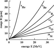
FIGURE 1.13 Penetration range in silicon of different particles as a function of energy. Reprinted with permission from Karnik et al. [12]. Copyright © 2004 IEEE.
Besides neutrons, other particles, such as pions and muons, exist in the terrestrial cosmic rays. However, neither pions nor muons are a significant threat to semiconductor devices. The number of pions is negligible compared to neutrons and therefore pions can cause far less upsets than neutrons. The kinetic energy of muons is usually very high, and muons do interact directly with electrons. Nevertheless, typically, muons do not create a sufficiently dense electron–hole trail to cause an upset. Ziegler and Puchner [30] predict that these particles can cause soft errors worth only a few FIT.
Critical Charge (Qcrit)
Stopping power explains why and how many electron–hole pairs may be generated by an alpha or a neutron strike, but it does not explain if the circuit will actually malfunction. The charge accumulation needs to cross a certain threshold before an SRAM cell, for example, will flip the charge stored in the cell. This minimum charge necessary to cause a circuit malfunction is termed as the critical charge of the circuit and represented as Qcrit. Typically, Qcrit is estimated in circuit models by repeatedly injecting different current pulses through the circuit till the circuit malfunctions.
Hazucha and Svensson [11] proposed the following model to predict neutron-induced circuit SER:
Constant is a constant parameter dependent on the process technology and circuit design style, Flux is the flux of neutrons at the specific location, Area is the area of the circuit sensitive to soft errors, and Qcoll is the charge collection efficiency (ratio of collected charge and generated charge per unit volume). It should be noted that the SER is a linear function of the neutron flux, as well as the area of the circuit. The parameter Qcoll depends strongly on doping and Vcc and is directly related to the stopping power. The greater is the stopping power, the greater is Qcoll. Qcoll can be derived empirically using either accelerated neutron tests or device physics models, whereas Qcrit is derived using circuit simulators. Although Hazucha and Svensson formulated this equation for neutrons, it can also be used to predict the SER of alpha particles. In reality, the SER equations used in industrial models can be far more complicated with a number of other terms to characterize the specific technology generation.
The Hazucha and Svensson equation does explain the basic trends in SERs over process technology. With every process generation, the area of the same circuit goes down, so this should reduce the effective SER encountered by a circuit scaled down from one process generation to the next. However, Qcrit also decreases because the voltage of the circuit typically goes down across process generations. At present, for latches and logic, this effect appears to cancel each other out, resulting in roughly a constant circuit SER across generations. However, if Qcrit is sufficiently low, such as seen in SRAM devices, which are usually 5–10 times smaller than latches in the same technology, then the impact of the area begins to dominate. This is usually referred to as the saturation effect, where the SER for a circuit decreases with process generations. Interestingly, however, the circuit is highly vulnerable to soft errors in the saturation region. In the extreme case, as Qcrit approaches zero, almost any amount of charge generated by alpha or neutron strikes will result in a transient fault.
Chapter 2 discusses in greater detail how to compute Qcrit and map it into a circuit-level SER.
1.8 Architectural Fault Models for Alpha Particle and Neutron Strikes
Microprocessors and other silicon chips can be considered to have different levels of abstractions: transistors that create circuits, circuits that create logic gates and storage devices, and finally the gates and storage devices themselves. The last few sections describe how a transistor collects charge from an alpha particle or a neutron strike. When this charge is sufficient to overwhelm a circuit, then it may malfunction. Logically, at the gate or cell level, this malfunction appears as a bit flip. For storage devices, the concept is simple: when a bit residing in a storage cell flips, a transient fault is said to have occurred (Figure 1.14).

For logic devices, however, a change in the value of the input node feeding a gate or output node coming out of a gate does not necessarily mean a transient fault has actually occurred. Only when this transient fault propagates to a forward latch or storage cell does one say a transient fault has occurred. Chapter 2 discusses transient faults in logic devices in greater detail.
An alpha particle or a neutron strike can, however, cause bit flips in multiple storage or logic gates. There are two types of multibit faults: spatial and temporal. Spatial multibit faults arise when a single neutron can cause flips in multiple contiguous cells. In today’s technology, such multibit faults primarily arise only in SRAM and DRAM cells because latches and clocked logic devices are significantly larger than these memory cells. Temporal multibit errors occur when two different neutron or alpha particles strike two different bits. Typically, these are related to error detection codes and are discussed in Chapter 5.
Maiz et al. [14] computed the probability of a spatial multibit error in 130- and 90-nm process technology for Intel SRAM cells based on experiments done under an accelerated neutron beam (Figure 1.15).8 The probability of an error in three or more contiguous bits is still quite low, but the double-bit error rate could be as high as 1–5% of the single-bit error rate. Such double-bit errors could arise because of not only the small size of transistors but also the aggressive layout optimizations of memory cells. As process technology continues to shrink, this effect will get worse and is likely to increase the number of spatial double-bit errors. Fortunately, current processors and chipsets can use interleaved error detection and correction codes to tackle such errors (see Chapter 5). For further details on multibit errors, please refer to recent analysis of multibit errors in CMOS technology by Seifert et al. [20].
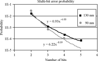
FIGURE 1.15 Probability of a multibit error compared to a single-bit error in a sample of SRAM cells. Reprinted with permission from Maiz et al. [14]. Copyright © 2003 IEEE.
1.9 Silent Data Corruption and Detected Unrecoverable Error
For an alpha particle or a neutron to cause a soft error, the strike must flip the state of a bit. Whether the bit flip eventually affects the final outcome of a program (Figure 1.3) depends on whether the error propagates without getting masked, whether there is error detection, and whether there is error detection and correction. Architecturally, the error detection and correction mechanisms create two categories of errors: SDC and DUE. Much of the industry has embraced this model because of two reasons. First, different market segments care to a different degree about SDC versus DUE. Second, this allows semiconductor manufacturers to specify what the error rates of their chips are.
The rest of this section explains these definitions, the subtleties around the definitions, and soft error budgets vendors typically create for their silicon chips.
1.9.1 Basic Definitions: SDC and DUE
Figure 1.16 illustrates the possible outcomes of a single-bit fault. Outcomes labeled 1–3 indicate nonerror conditions. The most insidious form of error is SDC (outcome 4), where a fault induces the system to generate erroneous outputs. SDC can be expressed as both FIT and MTTF. To avoid SDC, designers often use basic error detection mechanisms, such as parity.
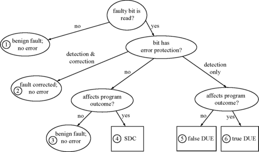
FIGURE 1.16 Classification of the possible outcomes of a faulty bit in a microprocessor. Reprinted with permission from Weaver et al. [26]. Copyright © 2004 IEEE.
The ability to detect a fault but not correct it avoids generating incorrect outputs, but cannot recover when an error occurs. In other words, simple error detection does not reduce the overall error rate but does provide fail-stop behavior and thereby avoids any data corruption. Errors in this category are called DUE. Like SDC, DUE is also expressed in both FIT and MTTF. Currently, much of the industry specifies SERs in terms of SDC and DUE numbers.
DUE events are further subdivided according to whether the detected fault would have affected the final outcome of the execution. Such benign detected faults are called false DUE events (outcome 5 of Figure 1.16) and others true DUE events (outcome 6). A conservative system that signals all detected faults as processor failures will unnecessarily raise the DUE rate by failing on false DUE events. Alternatively, if the processor can identify false DUE events (e.g., the fault corrupted only the result of a wrong-path instruction), then it can suppress the error signal.
DUE events can also be divided into process-kill and system-kill categories (not shown in Figure 1.16). In some cases, such as a parity error on an architectural register, an OS can isolate the error to a specific process or set of processes. The OS can then kill the affected process or processes but leave the rest of the system running. Such a DUE event is called process-kill DUE. The remaining DUE events fall into the system-kill DUE category, as the only recourse is to bring down the entire system.
A silicon chip had an initial SDC of 1000 FIT purely from soft errors. The vendor decided to add parity to every bit that contributed to the 1000 FIT SDC. The vendor also estimated that the false DUE per bit will cause a DUE increase of 20%. What is the resulting DUE of the chip? Assume only single-bit faults.
SOLUTION Adding parity to the chip converts SDC to DUE. So, the total DUE of the chip would be (1 + 0.2) × 1000 = 1200 FIT.
There are four subtleties in the definitions of SDC and DUE. First, inherent in the definition of a DUE event is the idea that it is a fail-stop. That is, on detecting the error, the computer system prevents propagation of its effect beyond the point at which it has been detected. Typically, a computer system can reboot—either automatically or manually—and return to normal function after a DUE event. That may not necessarily be true for an SDC event.
Second, because a DUE event is caused by an error detected by the computer system, it is often possible to trace back to the point where the error occurred (see Chapter 5). A computer system will typically or optionally log such an event either in hardware or in software, allowing system diagnosis. In contrast, it is usually very hard to trace back and identify the origin of an SDC event in a computer system. Logs may be missing if the system crashes due to an SDC event before the computer has a chance to log the error.
Third, a system crash may not necessarily be a DUE event. An SDC event may corrupt OS structures, which may lead to a system crash. System crashes that are not fail-stop—that is, the effect of the error was not detected and its propagation halted—are usually classified as SDC events.
Finally, a particle strike in a bit can result in both SDC and DUE events. For example, a bit may have an error detection scheme, such as parity, but the parity check could happen a few cycles after the bit is read and used. The hardware can clearly detect the error, but its effect may already propagate to user-visible state. Conservatively, soft errors in this bit can be classified always as SDC. Alternatively, soft errors in this bit can be binned as SDC during the vulnerable interval where its effect can propagate to user-visible state and DUE after parity check is activated. The latter needs careful probabilistic analysis.
1.9.2 SDC and DUE Budgets
Typically, silicon chip vendors have market-specific SDC and DUE budgets that they require their chips to meet. This is similar in some ways to a chip’s power budget or performance target. The key point to note is that chip operation is not error free. The soft error budgets for a chip would be set sufficiently low for a target market such that the SDC and DUE from alpha particles and neutrons would be a small fraction of the overall error rate. For example, companies could set an overall target (for both soft and other errors) of 1000 years MTTF or 114 FIT for SDC and 25 years MTTF or about 4500 FIT for DUE for their systems [16]. The SDC and DUE due to alpha particle and neutron strikes are supposed to be only a small fraction of this overall budget.
Table 1.1 shows examples of SDC and DUE tolerance in sample application servers. For example, databases often have error recovery mechanisms (via their logs) and can often tolerate and recover from detected errors (see Log-Based Backward Error Recovery in Database Systems, p. 317, Chapter 8). But they are often not equipped to recover from an SDC event due to a particle strike. In contrast, in the desktop market, software bugs and device driver crashes often account for a majority of the errors. Hence, processors and chipsets in such systems can tolerate more errors due to particle strikes and may not need as aggressive a protection mechanism as those used in mission-critical systems, such as airplanes. Mission-critical systems, on the other hand, must have extremely low SDC and DUE because people’s lives may be at stake.

A system is to be composed of a number of silicon chips, each with an SDC MTTF of 1000 years and DUE MTTF of 10 years (both from soft errors only). The system MTTF budgets are 100 years for SDC and 5 years for DUE. What is the maximum number of chips that can fit into the overall soft error budget?
SOLUTION 10 chips can fit under the SDC budget (= 1000/100) and two chips under the DUE budget (= 10/5). Hence, the maximum number of chips that can be accommodated is two chips.
If the effective FIT rate of a latch is 0.1 milliFIT, then how many latches can be accommodated in a microprocessor with a latch SDC budget of 10 FIT?
SOLUTION Total number of latches that can be accommodated is 100 000 (= 10/0.0001). The Fujitsu SPARC64 V processor (announced in 2003) had 200 000 latches [2]. Modern microprocessors can have as many as 10 times greater number of latches as that in the Fujitsu SPARC64 V. Consequently, it becomes critical to protect these latches to allow the processor to meet its SDC budget.
1.10 Soft Error Scaling Trends
The study of computer design and silicon chips necessitates prediction of future scaling trends. This section discusses current predictions of soft error scaling trends in SRAM, latches, and DRAM cells. As with any prediction, these could be proven incorrect in the future.
1.10.1 SRAM and Latch Scaling Trends
As explained in the Critical Charge (Qcrit) subsection in this chapter, there are two opposite effects that determine the SER of circuits, such as SRAM cells or latches. An SRAM cell typically consists of six transistors that make up two cross-coupled inverters that store the memory value and a couple of transistors that connect the input and output to the bitlines. As transistor and hence SRAM cell size continues to shrink across process technologies, the SER should reduce because a neutron has a less cross-sectional area to strike and cause a malfunction. However, as the cell size decreases, it holds less charge causing the Qcrit to decrease. This makes it easier for the cell to be upset due to a neutron strike. Figure 1.17 shows that these opposing effects mostly cancel each other out, and overall there is a slight decrease in SRAM SER. This suggests that SRAM cells approach the “saturation” region in which any strike would potentially cause a soft error (because of a sufficiently low Qcrit).

FIGURE 1.17 SRAM scaling trend. a.u. = arbitrary units. BPSG refers to boron contamination that could increase neutron-related errors. The graph shows that the FIT/bit for SRAM cells in recent times (toward the right end of the graph) decreases slowly over time. Vdd is the supply voltage of the chip. Reprinted with permission from Baumann [3]. Copyright © 2002 IEEE.
Overall, the FIT/bit of SRAM storage appears be in the range of 1–10 milliFIT [17,25]. The relatively large variation in the FIT rate arises primarily due to the variation in size, supply voltage, collection efficiency, and other process-related parameters of an SRAM cell. In contrast, the SER for latches appears to be roughly constant (or to vary within a narrow band) over the past few generations since they have not approached the saturation region yet [8].
The SER of other logic devices are, however, predicted to increase over technology generations. SER of logic devices, such as NAND and NOR gates, are typically lower than those of storage elements, such as SRAM cells or latches, because the effects of most alpha particle or neutron strikes are masked. For example, the glitch created at a gate by a strike may not propagate to a forward latch to cause an error. This is known as electrical masking. As the number of logic levels shrinks and the frequency of chips increases, this masking effect is reduced causing more soft errors. Chapter 2 discusses soft error trends in logic devices in greater detail.
Overall, to the first approximation today, the SER of a silicon chip is a function of the number of unprotected latches and SRAM cells in the chip. Because the total number of bits in a microprocessor—both protected and unprotected—roughly doubles every technology generation, one can expect the SER to roughly double, unless significant soft error protection techniques are designed into the microprocessor.
1.10.2 DRAM Scaling Trends
Figure 1.18 shows the scaling trends in DRAMs. DRAM cells are typically made of four transistors (as opposed to six-transistor SRAMs). Large main memory systems are made up of DRAM chips. Typically, a DRAM device consists of 256–1024 megabits in current technology. A number of these devices are, in turn, put in a dual-interlocked memory module (DIMM), which connects to the processor motherboard. DIMMs of 1 gigabyte are not uncommon today in desktops and laptops. Total DRAM capacity in a server machine can be as high as 512 gigabytes.

FIGURE 1.18 DRAM scaling trends. a.u. = arbitrary unit. This graph shows the DRAM FIT/bit decreases exponentially with every DRAM device generation, but the FIT/device has remained roughly constant in recent times. Reprinted with permission from Baumann [3]. Copyright © 2002 IEEE.
DRAM and SRAM scaling trends differ significantly. Vendors have successfully reduced the FIT/bit of DRAMs exponentially as the number of bits per DRAM device has increased. The FIT per DRAM device, however, appears to have stayed roughly constant over generations. DRAM vendors have achieved this by digging deeper trenches, adding more stacks, using thinner and alternate dielectrics, and putting bigger capacitors on the DRAM cells. This has allowed the collected charge to decrease without decreasing Qcrit.
Although the DRAM FIT per device has remained constant, large servers with significant amounts of memory may still have significant error rates. Further, because the amount of memory used can be very large, DRAM can also encounter multiple bit errors. Appropriate fault detection and error correction techniques must be used to tackle these errors.
1.11 Summary
Radiation-induced transient faults are caused by alpha particles found in chip packages and atmospheric neutrons. A soft error is a manifestation of a transient fault. Soft errors due to alpha particles in silicon chips were first reported by Intel Corporation in 1979, and soft errors due to neutrons were first reported by IBM Corporation in 1984. Since then computer system problems caused by alpha particles and neutrons have been reported intermittently.
MTTF is a common metric used to express the SER from alpha particles and neutrons. The MTTF of a system composed of multiple components is the inverse of the sum of the inverse of the component MTTFs. The inverse of MTTF can also be expressed as FIT rates. One FIT represents an error in a billion hours. FIT rates are additive under the exponential failure law, which is commonly used in soft error analysis.
A soft error can be classified either as SDC or DUE. An SDC event arises when corrupted data eventually become visible to the user. A DUE event arises when the system detects a fault. The DUE typically assumes a fail-stop behavior in which an SDC event can never occur. Thus, the SER can be expressed as either the SDC MTTF or DUE MTTF, as the case may be.
Radiation-induced transient faults is one of many silicon reliability problems faced by the chip industry today. Other types of faults include permanent faults caused by EM and gate oxide breakdown and transient faults caused by transistor variability, thermal cycling, and erratic fluctuations of minimum voltage at which a circuit is functional. Radiation-induced transient faults are, however, the only ones that are typically dealt with directly in the field with fault detection and error correction circuitry.
Although alpha particles and neutrons are both classified as radiation, they arise from different sources. Alpha particles arise from chip packaging material. In contrast, neutrons emanate when primary, secondary, and tertiary cosmic rays collide with the atmosphere. Neutrons from galactic particles, instead of solar particles, are the dominant source of neutrons on the earth’s surface.
An alpha particle causes a malfunction in a circuit’s operation when it penetrates a crystal and loses sufficient energy in a transistor’s substrate to create electron–hole pairs that are swept into the diffusion regions of the transistor. The amount of energy lost or released by an alpha particle per unit track length in a silicon crystal is known as the stopping power. Stopping power varies with kinetic energy of an alpha particle. The greater the kinetic energy of an alpha particle, the less is its stopping power and hence the amount of energy released in a silicon crystal.
Neutrons do not interact with the silicon crystal to create electron–hole pairs. Instead, neutrons can undergo inelastic collisions with the silicon crystal, which can produce alpha particles and carbon (12C) nuclei. A carbon nucleus has a low energy but a high stopping power in a silicon crystal. This carbon nucleus can generate sufficient electron–hole pairs to cause a transistor malfunction.
The charge generated by alpha particles and neutrons must be higher than the minimum charge necessary to cause circuit malfunction. This minimum charge is known as the critical charge and expressed as Qcrit. As transistors shrink in size with every process technology generation, they hold less charge, thereby causing a lower Qcrit and making them more vulnerable to a particle strike. However, with every technology generation, the transistors also shrink in size making them harder to strike. For latches, these effects often cancel out, roughly giving a constant FIT/bit over technology generations. For SRAM cells, the transistor has shrunk to an extent that most particle strikes on such a cell will cause a bit flip. Hence, the SER of an SRAM cell continues to decrease with every process technology. DRAMs have, however, managed to aggressively decrease the FIT/bit using various optimizations not typically available for SRAM cells or latches.
1.12 Historical Anecdote
The first half of the 20th century saw a flurry of research into radiation physics. In the 1890s Wilhelm Conrad Roentgen discovered X-rays, for which he received the first Nobel Prize for physics in 1902. Scientists discovered that X-rays and other radioactive materials ionize gases, which enabled these gases to conduct electricity. This effect was used to measure radiation using electroscopes. Scientists soon discovered that the charge in these electroscopes leaked away over time, no matter how they designed the electroscopes or what shielding they used around them. In 1912, an Austrian physicist named Victor Hess took an electroscope to a higher altitude in balloon flights and observed that the intensity of the ionizing radiation initially decreased with altitude, but by about 5000 feet, the radiation was more intense than that at sea level. Victor Hess surmised that this was due to cosmic radiation coming from beyond the earth’s atmosphere. Since then, the change in cosmic radiation flux with altitude has typically been used as the signature to identify cosmic rays. The term “cosmic rays” was, however, introduced later in 1926 by an American physicist named Robert Millikan.
References
Agostinelli M., Hicks J., Xu J., Woolery B., Mistry K., Zhang K., Jacobs S., Jopling J., Yang W., Lee B., Raz T., Mehalel M., Kolar P., Wang Y., Sandford J., Pivin D., Peterson C., DiBattista M., Pae S., Jones M., Johnson S., Subramanian G. Erratic Fluctuations of SRAM Cache Vmin at the 90 nm Process Technology Node. IEEE International Electron Devices Meeting (IEDM). December 2005:655–658.
Ando H., Yoshida Y., Inoue A., Sugiyama I., Asakawa T., Morita K., Muta T., Motokurumada T., Okada S., Yamashita H., Satsukawa Y., Konmoto A., Yamashita R., Sugiyama H. A13 GHz Fifth Generation SPARC64 Microprocessor. IEEE Journal of Solid State Circuits. November 2003;Volume 38(Issue 11):1896–1905.
Baumann R. Tutorial on Soft Errors. International Reliability Physics Symposium (IRPS) Tutorial Notes. IEEE, Dallas, Texas, USA. April 2002.
Baumann R., Hossain T., Smith E., Murata S., Kitagawa H. Boron as a Primary Source of Radiation in High Density DRAMs. IEEE Symposium on VLSI. June 1995:81–82.
Borkar S. Designing Reliable Systems from Unreliable Components: The Challengesof Transistor Variability and Degradation. IEEE Micro. November/December 2005;Volume 25(Issue 6):10–16.
Bossen D. CMOS Soft Errors and Server Design. International Reliability Physics Symposium (IRPS) Tutorial Notes. IEEE, Dallas, Texas, USA. April 2002.
Friedlander M.W. A Thin Cosmic Rain: Particles from Outer Space. Harvard University Press, November 2002.
Hareland S., Maiz J., Alavi M., Mistry K., Walstra S., Dai C. Impact of CMOS Process Scaling and SOI on the Soft Error Rates of Logic Processes. Symposium on VLSI Technology Digest of Technical Papers. June 2001:73–74.
Gordon M.S., et al. Measurement of the Flux and Energy Spectrum of Cosmic-Ray Induced Neutrons on the Ground. IEEE Transactions on Nuclear Science. December 2004;Vol. 51(No. 6):3427–3434. Part 2
Havekort B.R., et al. Performability Modelling: Techniques and Tools. John Wiley and Sons, 2001.
Hazuchaand P., Svensson C. Impact of CMOS Technological Scaling on the Atmospheric Neutron Soft Error Rate. IEEE Transactions on Nuclear Science. December 2000;Vol. 47(No. 6):2586–2594.
Karnik T., Hazucha P., Patel J. Characterization of Soft Errors Caused by Single Event Upsets in CMOS Processes. IEEE Transactions on Dependable and Secure Computing. April–June 2004;Vol. 1(No. 2):128–143.
JEDEC Standard. Measurement and Reporting of Alpha Particles and Terrestrial Cosmic Ray-Induced Soft Errors in Semiconductor Devices. JESD89. August 2001.
Maiz J., Hareland S., Zhang K., Armstrong P. Characterization of Multi-Bit Soft Error Events in Advanced SRAMs. Digest of International Electronic Device Meeting (IEDM). December 2003:21.4.1–21.4.4.
May T.C., Woods M.H. Alpha-Particle-Induced Soft Errors in Dynamic Memories. IEEE Transactions on Electronic Devices. January 1979;Vol. 26(Issue 1):2–9.
Michalak S.E., Harris K.W., Hengartner N.W., Takala B.E., Wender S.A. Predicting the Number of Fatal Soft Errors in Los Alamos National Laboratory’s ASC Q Supercomputer. IEEE Transactions on Device and Materials Reliability. September 2005;Vol. 5(No. 3):329–335.
Normand E. Single Event Upset at Ground Level. IEEE Transactions on Nuclear Science. December 1996;Vol. 43(No. 6):2742–2750.
Pradhan D.K. Fault-Tolerant Computer System Design. Prentice-Hall, 2003.
Reis G., Chang J., Vachharajani N., Rangan R., August D., Mukherjee S.S. Design and Evaluation of Hybrid Fault-Detection Systems. International Symposium on Computer Architecture (ISCA). June 2005:148–159. Madison, Wisconsin, USA
Seifert N., et al. Radiation-Induced Soft Error Rates of Advanced CMOS Bulk Devices. 44th Annual International Reliability Physics Symposium (IRPS). 2006:217–225.
Srinivasan G.R. Modeling the Cosmic-Ray-Induced Soft-Error Rate in Integrated Circuits: An Overview. IBM Journal of Research and Development. January 1996;Vol. 40(No. 1):77–89.
Strathis J.H. Reliability Limits for the Gate Insulator in CMOS Technology. IBM Journal of Research and Development. March/May 2002;Vol. 46(No. 2/3):265–286.
Segura J., Hawkins C.F. CMOS Electronics: How It Works, How It Fails. Wiley-IEEE Press, 2004.
Tang H.H.K. Nuclear Physics of Cosmic Ray Interaction with Semiconductor Materials: Particle-Induced Soft Errors from a Physicist’s Perspective. IBM Journal of Research and Development. January 1996;Vol. 40(No. 1):91–108.
Tosaka Y., Satoh S., Suzuki K., Suguii T., Ehara H., Woffinden G.A., Wender S.A. Impact of Cosmic Ray Neutron Induced Soft Errors, on Advanced Submicron CMOS Circuits. VLSI Symposium on VLSI Technology Digest of Technical Papers. June 1996:148–149.
Weaver C., Emer J., Mukherjee S.S., Reinhardt S.K. Techniques to Reduce the Soft Error Rate of a High-Performance Microprocessor. 31st Annual International Symposium on Computer Architecture. June 2004:264–275.
Wood A.P. Software Reliability from the Customer View. IEEE Computer. August 2003;Vol. 36(No. 8):37–42.
Ziegler J.F. Terrestrial Cosmic Rays. IBM Journal of Research and Development. January 1996;Vol. 40(No. 1):19–39.
Ziegler J.F., Lanford W.A. The Effect of Cosmic Rays on Computer Memories. Science. Vol. 206(No. 776), 1979.
Zielger J.F., Puchner H. SER—History, Trends and Challenges. Cypress Semiconductor Corporation, 2004.
1The half-life for a given particle is the time for half the radioactive nuclei in any sample to undergo radioactive decay.
21 eV is a unit of energy equal to the work done by an electron accelerated through a potential difference of 1 V.
3The Web site http://www.seutest.com provides a calculator to compute the neutron flux at a location based on a variety of parameters, such as latitude, longitude, altitude, and geometric rigidity (discussed later in this section).
4Terrestrial neutrons have two other peaks below the one between 10 and 1000 MeV. The other two peaks appear roughly between 0.01 and 0.02 eV (also called thermal neutrons) and between 0.01 and 5 MeV. These neutrons could also cause transient faults. Further, thermal neutrons may also arise in semiconductor processes that use the boron-10 isotope.
5In reality, the stopping power varies over its penetration distance (as expressed in µm) [21].
61 fC = 1 femto Coulomb = 10−15 C.