
CHAPTER 12
A Flexible Sequencer
Have you ever had a transmit-receive relay fail and witnessed the ensuing carnage that happens when you pump 100 W or more of RF into the front end of your multithousand-dollar receiver? Not a pretty sight. Dennis has experienced something similar to this with predictable results. In his case, it was a relay on the output of a very expensive 2 meter low noise amplifier (LNA) that was in the wrong position when the transmitter keyed up. You guessed it. The result was an ex-LNA.
If you spend much time around VHF and UHF “weak signal” work, referring to operating on CW or sideband, you eventually want to improve the performance of your station. The means to improving performance are simple: more power, more antenna gain, and more receiver gain. More power is easy, we add a high-power amplifier. Antennas? Well, bigger and higher Yagis come to mind. Receiver gain increases? We add an LNA. When we add amplifiers and LNAs we also need the means of controlling them, in other words, ways to switch them in and out of the circuit. By placing these items under control, we prevent things like what Dennis experienced when placing several hundred Watts of RF into the output of his very expensive LNA. What we need is a sequencer. Figure 12-1 shows the completed sequencer that is the subject of this chapter.
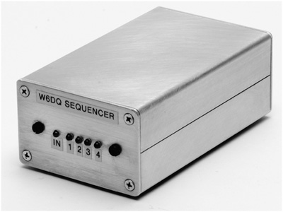
FIGURE 12-1 The flexible sequencer.
Just What Is a Sequencer?
Just like the name implies, a sequencer is a device that can turn other devices on and off in a specified order. A typical sequencer has four outputs that can be energized in order with an ever-so-slight delay between each output turning on, and then can de-energize the four outputs in the reverse order, with the same ever-so-slight delay between each output turning off. Why four outputs? The answer is pretty simple. You generally have four items that you want to control, namely, a low-noise amplifier, a transmit-receive relay, a high-power amplifier, and of course, the transmitter and receiver or transceiver, or possibly a transverter. Most sequencers have fixed time delays between outputs, say 100 ms. For most operations, 100 ms are more than enough time for things like relays to settle out after switching (they do take time to stop bouncing around after switching) and we do want them settled before applying the high-power RF. So, a sequencer is a pretty essential item in a high-power, weak-signal VHF/UHF station.
However, VHF/UHF stations are not the only place sequencers are used. Even on HF, if you are using a high-power linear amplifier, keying the amplifier in sequence with an antenna changeover relay is not a bad idea. Sequencers do have multiple applications in an amateur radio station.
The Sequencer Design
The sequencer shield described here is based on the relay shield constructed in Chapter 11. You can use the relay shield as it was built, with a few minor additions, connecting the external devices using the screw terminals, or you can use an alternative approach, which we describe later in this chapter. In the latter case, we provide a design that is “purpose built.” That is to say, it is a complete system, down to an enclosure to house it.
We chose not to use an Arduino board and shield; rather, the Digispark (as was used in Chapter 7 for the Keyer) seemed to be the perfect fit for this project. With six digital IO ports available on the Digispark, we can use one port as an input, four ports to drive the four relays, and the remaining port to drive an LED indicating there is an input signal present. (You could also use an ATtiny85 and program it as we did in Chapter 7. The Digispark, however, is a little easier to use because of its built-in USB port. The Arduino Nano 3.0 also offers a small footprint and attached USB port.) All four relays have LEDs to show their state.
The sequencer is shown in schematic form in Figure 12-2. For the sake of simplicity, the diagram depicts only one relay section, as shown within the dashed outline. There are three additional relay sections that are not shown, but are identical to the relay section shown in the diagram. Module A1 in Figure 12-2 is the Digispark (or an ATtiny85) and IC U1 is the hex driver (DS75492).
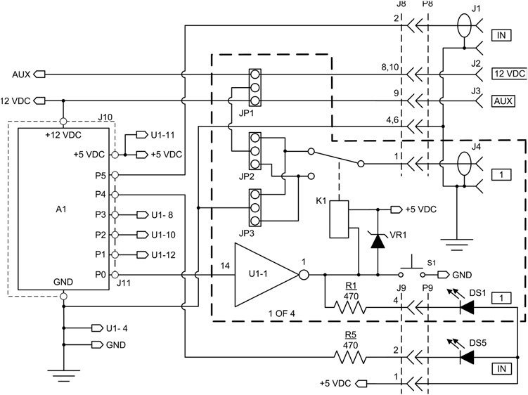
FIGURE 12-2 Sequencer schematic diagram using Digispark.
We have tried to create a flexible design, one that allows use of different voltage relays (we have a mix of 5, 12, and 24 VDC relays in use), different keying schemes (some pieces of equipment may require a grounded input to operate while others require a circuit to open). However, unlike the relay shield, we have added jumpers JP1 through JP12 to allow reconfiguration of the shield for normally open, normally closed, contacts to ground, to 12 VDC or to an auxiliary input that might use 24 VDC, a common voltage used for coaxial relays. There is no reason why the jumpers couldn’t be replaced with hardwired connections for your specific needs, simplifying construction.
Timing
The software is designed to allow the timing to be easily changed for each relay as well as the order in which the relays are energized and de-energized. This adds another layer of flexibility not found in the typical commercially-available sequencers. To help visualize what the output of the sequencer looks like, a representative timing diagram is shown in Figure 12-3. As the input goes to TRUE, each output is enabled in sequence. When the input goes to FALSE, each output is disabled in sequence. The sequence depicted is the default ordering of the outputs. The software is designed to allow the sequence to be changed easily.
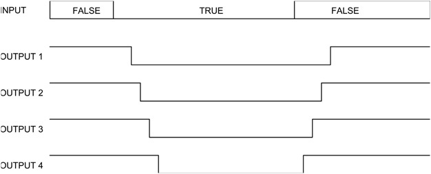
FIGURE 12-3 Default timing for the sequencer.
Constructing the Sequencer
As we mentioned earlier, we provide two methods of construction. First, we present a purpose-built design that is not assembled as a shield and is mounted in a nice enclosure. As an alternative, the relay shield from Chapter 11 can be used with several minor modifications and can be used with a second sketch described later in this chapter and shown in Listing 12-2.
A Purpose-Built Sequencer
The sequencer is constructed on a small 5 cm by 7 cm (approximately 2 in. × 2.75 in.) prototyping board obtained on eBay and is housed in an extruded Aluminum chassis with removable front and rear panels. This particular prototyping board is quite nice in that it is double sided with plated-through holes, making construction much easier. The extruded aluminum enclosure is an LMB product, EAS-100, and is available in plain aluminum or black anodized finish (see: http://www.lmbheeger.com/products.asp?catid=68). These enclosures are quite nice for small projects and reasonably priced. It consists of two interlocking extruded aluminum pieces (top and bottom) that include slots for mounting circuit boards, with two aluminum plates that screw on for a front and rear panel. You can see the enclosure in Figure 12-1. We drilled mounting holes in the bottom half of the enclosure for the circuit board; mounting holes in the rear panel for the RCA jacks and power connectors; and mounting holes in the front panel for the circuit board and LEDs.
As mentioned earlier, rather than using an Arduino, this version is constructed using an Arduino “clone,” a Digispark board. Refer back to Figure 12-2 to view the schematic for the sequencer. The parts list for the sequencer is shown in Table 12-1. Figure 12-4 shows parts placement for the sequencer and Figure 12-5 is the wiring diagram. As before, the wiring diagram shows the card from the bottom side.

FIGURE 12-4 Sequencer parts placement.
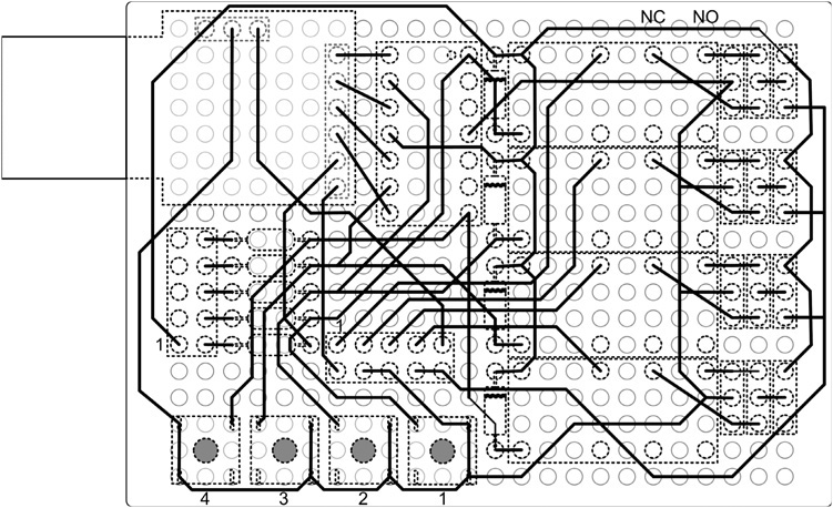
FIGURE 12-5 Sequencer wiring diagram.
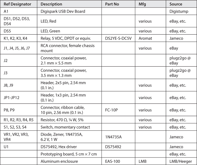
TABLE 12-1 Sequencer Parts List
The assembled sequencer board is shown in Figure 12-6. You can clearly see the configuration jumpers on the left side of the shield, the Digispark at the upper right, the pushbuttons near the bottom-right for manual operation, and the two 10-pin headers connecting to the front and rear panels. It’s a good idea to mark pin 1 of each header using a marker. We have permanently soldered the Digispark to the circuit board using header pins. If you are not comfortable mounting the Digispark in this manner, you can add header sockets to the Digispark to make it removable. (Don’t forget, you could also program an ATtiny85 to do the job.)
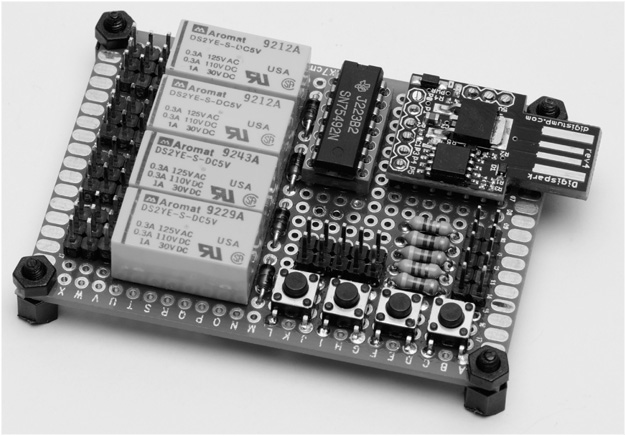
FIGURE 12-6 Assembled sequencer board.
One physical difference between the relay shield and this version of the sequencer is that the LEDs are mounted remotely on the front panel in order to be visible during operation. The LEDs are mounted on a smaller prototype board and connected to the main board with a ribbon cable. Figure 12-7 shows the front panel construction and how the prototype board is mounted. Mounting the LEDs is fairly simple. The first step is to drill the holes in the front panel for the LEDS and mounting screws. Next, place the LEDs in the appropriate locations on the prototyping board but do not solder them in place. The board is then mounted to the front panel and the LEDs slipped into their respective holes on the front panel. The LEDs are then soldered into place. (You could also mount the LEDs in rubber grommets on the front panel, but that is less robust than the approach used here.)

FIGURE 12-7 Front panel construction showing LEDs.
The rear panel is drilled for five RCA jacks and two coaxial power connectors. We used two different sized coaxial power connectors so they would not be mixed up in use. The rear panel is connected to the sequencer board using another piece of ribbon cable. We chose to use connectors on the ribbon cable for ease of disassembly; however, this is not required. The ribbon cables can be soldered in place if so desired. Figure 12-8 shows the rear panel of the sequencer. (You can often find old floppy drive ribbon cables for next to nothing at flea markets, hamfests, and even used items stores, like Goodwill or church-related shops.)
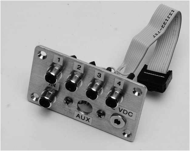
FIGURE 12-8 Sequencer rear panel construction.
The sequencer is shown assembled in Figure 12-9. You can clearly see the front and rear panels and the main sequencer board and how they are interconnected. A labeler was used for the finishing touches on the assembly.

FIGURE 12-9 Assembled sequencer.
Remember, before you ever apply power to the sequencer, you should check your wiring against the schematic and wiring diagrams. Use a continuity tester or multimeter for tracing the wiring. If you don’t have access to these, use a yellow highlighter to trace a copy of the schematic. Once you are satisfied that the wiring is correct, you can proceed with applying power and testing the sequencer.
To operate the sequencer, 12 VDC is applied to the 12 V coaxial input pin and an input that is normally open to ground is connected to the Input RCA jack.
Programming and Testing the Sequencer
In this section, we load the sequencer program into the Digispark and begin testing the completed sequencer. You need to review the programming procedure described in Chapter 7 for the Digispark keyer. Some of the important points to remember are that you must use IDE 1.04 with the Digispark extensions installed. The new Digispark Pro, which offers more memory and I/O pins, does work with later versions of the Arduino IDE. You must use the Arduino IDE that has been modified by Digistump for use with the Digispark. The sequencer program source code for the Digispark is shown in Listing 12-1.
LISTING 12-1 Sequencer program for Digispark.
Initial Testing of the Sequencer
If you have assembled the sequencer into an enclosure similar to what we have used, you need to provide access to the USB connector on the Digispark. One other recommendation that comes from the Digispark Wiki site: use a USB hub to apply power to the Digispark via USB rather than a direct connection to the USB. In the event that there is a short circuit in your wiring, you run the risk of damaging the USB port on your computer. Using a USB hub may blow the hub away, but at least the computer’s USB port is saved.
Now apply 12 VDC to the 12 V connector on the rear panel. If the Digispark you are using has never been programmed, none of the LEDs should be lit and none of the relays should have clicked. At this point, you should be able to check the relays and LEDs by pressing each pushbutton on the shield. If it all checks out, you can proceed with loading the sequencer program.
Loading the Sequencer Program and Testing
First, make sure that you have the 12 VDC power disconnected from your sequencer. Launch the Digispark IDE 1.04 with the Digispark extensions and load the sequencer sketch from Listing 12-1. Remember that you need to compile and upload with the Digispark disconnected from the USB port. The IDE prompts you when to connect the USB cable to the Digispark. Once the program is loaded, the IDE informs you that the load was successful.
To test the sequencer, apply a ground to the input pin (J1 in Figure 12-2). The four relays and corresponding LEDs will fire up in sequence. Releasing the switch causes the relays and LEDs to go off in the reverse sequence.
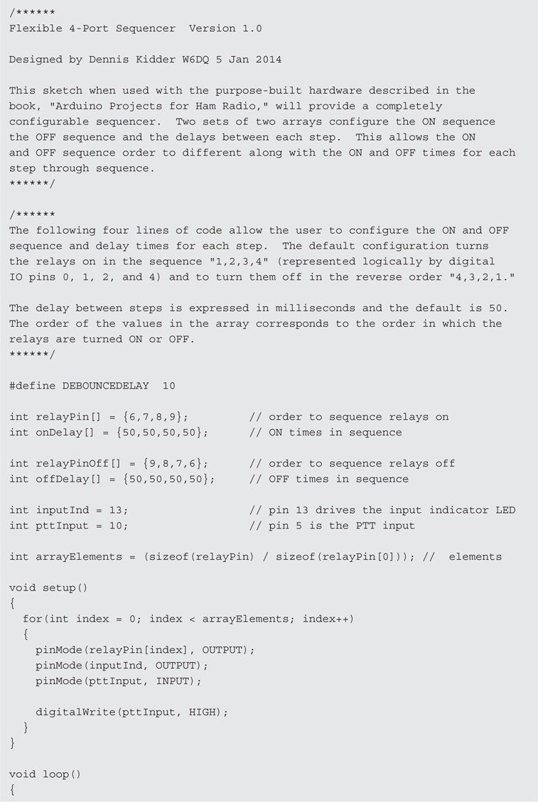
Sequencer Code “Walk-Through”
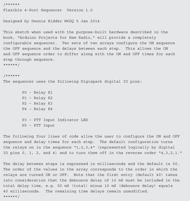
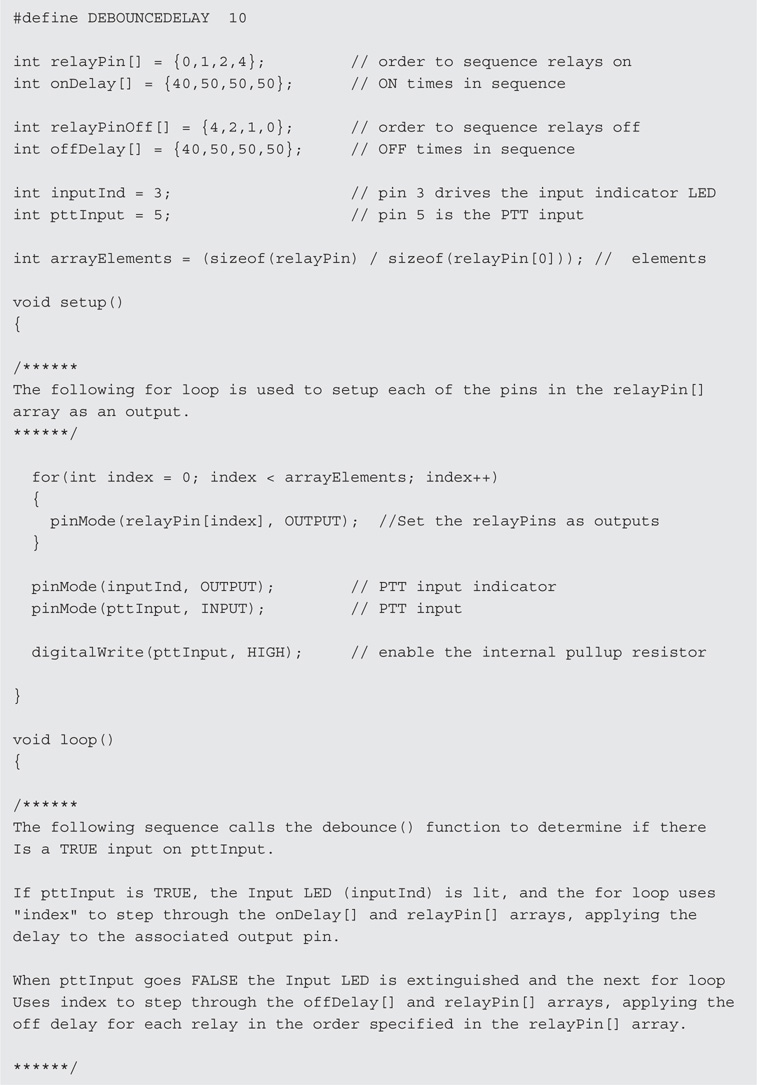
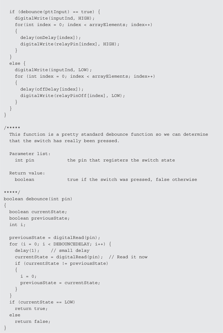
The sequencer code from Listing 12-1 should be pretty straightforward to you by now. We define DEBOUNCEDELAY as 10 ms. We then set up four arrays: relayPin[], onDelay[], relayPinOff[], and offDelay[], and populate them. As noted in the comments, the relayPin[] array sets the order in which the relays are turned on following the time delay set by onDelay[] for each relay. The first entry in onDelay[] corresponds to the first entry in relayPin[]. We also set up the pin numbers for the Input indicator LED and the PTT input pin. The following lines of code define the pin numbers for the PTT input (pttInput) and the PTT input indicator (inputInd):
![]()
We have to be careful when defining the pins as inputs and outputs with the Digispark. There are multiple pins that serve multiple purposes. The USB interface is realized with P3 and P4. P3 causes problems for us under certain circumstances as it has a 1.5K pull-up resistor connected. Placing a load on P4 may cause the USB to not function. P1 has an on-board LED. If we use this as an output, we have to consider the extra load from the on-board LED. Fortunately, there is a circuit trace that can be cut to disable the LED, which we have done for this application. Cutting the trace to disable the LED is described in the Digispark Wiki:
http://digistump.com/wiki/digispark
In addition, the power indicating LED on the Digispark also has a trace that may be cut in order to reduce current consumption. P5 brings its own quirks to the table in that it is designed as a 3.3 V level output. While we can use P5 as an output, it seemed more reasonable to us to use it as the PTT input.
Next we determine the number of members in the arrays. When the compiler creates the array in memory, it allocates memory based on the number of elements and their data type. In this case, the members are all integers. This line of code:
int arrayElements = (sizeof(relayPin) / sizeof(relayPin[0]));
sets arrayMembers to the number of elements calculated to be in the relayPin array. sizeof() is actually a C operator used to determine the number of bytes occupied by an array or a variable data type. Although using sizeof() looks like a function call, it isn’t. By dividing sizeof(relayPin) by sizeof(relayPin[0]), we know how many elements are in the array. All four arrays contain integers and by necessity, the same number of members and as a result, all four arrays are the same size. Using this approach means that we can change the array sizes or data types if need be and all of the loops that need to use the array size are automatically adjusted for us via the variable arrayElements.
In the void setup() section, we use the relayPin[] array to initialize each of the relay pins as an output. The for loop marches through each position in the array according to the value of index. Take a look at the for loop:
for(int index = 0; index < arrayElements; index++)
The value of index is incremented from “0” (zero) and used as a pointer to the array element, and then sets each element of the relayPin array as an OUTPUT. When the value of index increments and is no longer less than the number of elements in the array, the loop terminates.
We initialize the inputInd and the pttInput pins next. We use the last step in the sequence, a digitalWrite() to the input pin which may seem counter-intuitive but is most useful. By setting the input pin HIGH with the digitalWrite(), we enable an internal pullup resistor in the Digispark on the input pin, eliminating the need for an additional external pullup resistor.
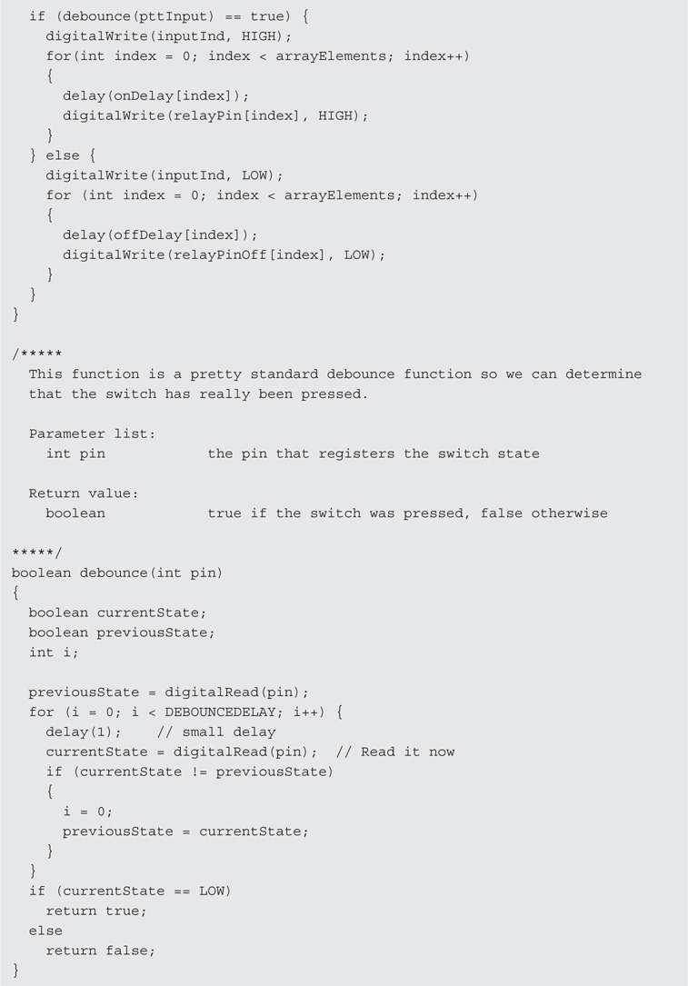
The void loop() section of the program applies the associated on and off time delay to each relay in the sequence specified by the relayPin[] and relayPinOff[] arrays. We use the same debounce function that was used in the Real Time Clock/Timer sketch from Chapter 4. While the debounced pttInput pin is TRUE, we execute the for loop as we did above, incrementing through each element of the onDelay and relayPin arrays and following the specified delay, setting each pin HIGH, turning on the relay.
When pttInput goes FALSE, a second for loop increments through each element of the offDelay[] and relayPinOff[] arrays, and following the specified delay, sets each pin LOW, turning off each relay.
Modifying the Sequence Order and Delay Time
The sequencer program is designed to allow the user to easily modify the order in which the relays turn on and off, as well as the time delay between each step. There are only four lines of code that you might need to modify:
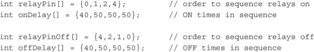
The first line sets the order in which the relays are energized. It is highly likely that you would not need to modify this line, but you can if need be. (Remember that the initializer list uses logical pins, not the relay number.) The second line sets the delay in milliseconds between each relay being energized. Of course, the first entry is the time delay from when the input is detected. We have set this up so that each delay is individually configurable and corresponds to the relay order from the previous line.
So why is the first delay 40 ms instead of 50? The first entry should be reduced by 10 ms as dictated by the debounce delay. The debounce function introduces the time delay defined by DEBOUNCEDELAY, in this case, 10 ms. The debounce delay must elapse before the first entry of the on or off time delay arrays are executed. In other words, if the first entry is set to 0 (zero), the first relay is energized 10 ms following the detection of an input because the debounce delay does not provide a return until 10 ms have elapsed from a change of state of the input. As a result, since we want the default delay to be 50 ms, we must subtract the 10 ms from the first entry, hence a value of 40 ms.
The third and fourth lines are used to configure the order and time delays for de-energizing the relays. The default configuration de-energizes the relays in the opposite order to which they were energized. This can be changed to meet any special requirements you may encounter in your application. As we have shown in the default configuration, the first entry includes the 10 ms debounce delay.
Configuring the Jumpers for Different Situations
The sequencer is designed to fit into a lot of different configurations. In a typical ham station, we might encounter 28 V antenna relays as well as 12 V or even 115 VAC relays. We might have components that require a ground to be actuated or require switched 12 VDC input. The jumpers allow us to configure the output of the sequencer to accommodate many different requirements.
The RCA output jacks are connected to the center contact of each relay and each relay has a normally open (NO) and normally closed (NC) position. There are three possible selections for the NO or NC position: 1) Ground, 2) +12 VDC, or 3) AUX. AUX selects an arbitrary voltage applied to the AUX input on the rear panel. This could be 28 VDC (or AC). We would not recommend switching a 115 VAC circuit (even though the relays are rated for 1 A at 115 VAC), but would recommend using an external relay to switch the higher voltage. Figure 12-10 shows the six possible jumper positions for each output. Note that only the pins for relay K1 are shown. The other three relay’s jumper pins are identical.
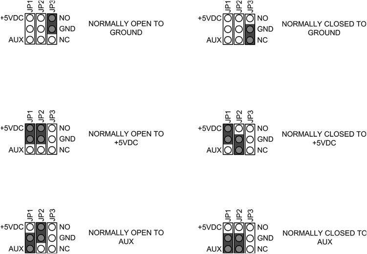
FIGURE 12-10 Jumper configurations.
Modifying the Relay Shield from Chapter 11
To use the relay shield from Chapter 11, we make several simple additions. The additions consist of adding an input connection to the Arduino with which to trigger the sequencer. We have added another set of screw terminals for input interface, mounting a two-position screw terminal in the 40-pin header area of the shield. (The new terminal is near the right edge of the board shown in Figure 12-11.) One pin of the screw terminal is wired to ground and the other pin is wired to Digital IO pin 10. The new input detects a normally open circuit that would close to ground, such as a push-to-talk (PTT) switch on a microphone. You can also add the LED used to indicate that an input is present. You can use Digital IO pin 13 to drive this LED. Be sure to add a 1K resistor in series with the LED. You may also wish to mount the LEDs remotely, rather than on the relay shield as it is shown in Chapter 11.
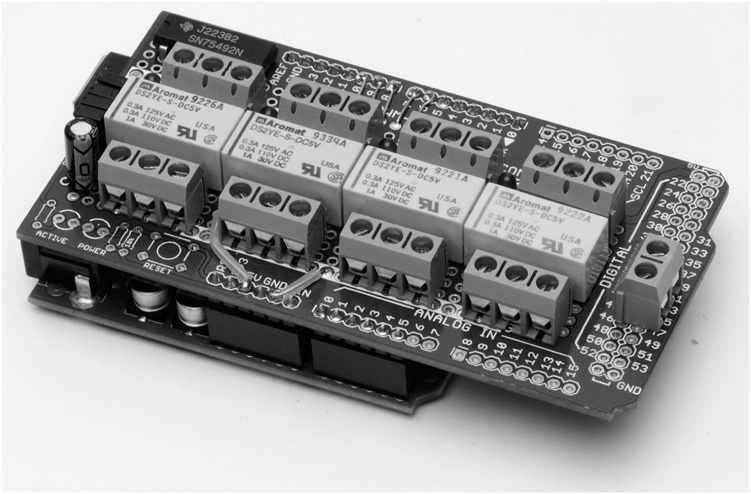
FIGURE 12-11 New screw terminal added to the relay shield (far right).
Figure 12-11 shows the location of the new screw terminals (compare to Figure 11-3). As this version is built as a shield, it is operated with an Arduino. The modified relay shield is shown being used with an Arduino Duemilanove, but the shield can be used with virtually any Arduino or compatible. CAUTION: When using the Mega shield with most Arduinos, be sure to cover the USB connector with insulating material, preferably two layers of black electrical tape. The Mega shield (and several others we might add) allows you to mount components in the area directly above the USB connector leading to the possibility of a short circuit if a component lead or wiring comes in contact with the USB connector.
Alternate Listing for the Relay Shield Sequencer
We have provided an alternate source code version of the sequencer program sketch for use with the modified relay shield and an Arduino. The alternate version is shown in Listing 12-2. The modifications are limited to changing pin assignments from what were used the Digispark version to those that are used with the Chapter 11 relay shield and an Arduino. Follow the same testing procedure for the modified relay shield that was used for testing the Digispark sequencer. Once you are satisfied that the shield is wired correctly you can proceed with loading the program in Listing 12-2 and continue with testing.
LISTING 12-2 Sequencer program for Arduino.
Conclusion
In this chapter we have constructed a device that can now be integrated into the user’s station. It is a matter of determining the switching requirements of the attached devices and configuring the sequencer’s jumper pins to match those requirements. One thing that has not been covered in this chapter is dealing with RF interference. It is always possible that stray RF signals can enter the sequencer’s enclosure and cause indeterminate results. The aluminum enclosure we used does a pretty good job of shielding the contents, but in the event that RF does get in, then you might try adding a small capacitor across each input and output, and power connectors (.01 μF at 50 V should suffice). Other measures include reviewing the grounding on the station, using well-shielded RCA patch cables, and possibly adding clamp-on ferrite EMI suppressors to the cables. The combination of clamp-on ferrite and capacitor on each cable and jack should take care of any issues you may encounter.
Last but not least, this design is made to be expandable. If you should need more than four outputs, it is quite easy to add additional relays, up to six, without having to add another hex driver. Of course, if you need more relays, you cannot use the Digispark1 version because of the limit number of I/O line. In such cases, you will have to use the Arduino shield version. Adding relays means adding elements to the arrays, making sure they are added in equal numbers to all of the affect arrays.
We are certain that you will discover new applications for the sequencer in your radio shack. It’s up to you to explore the possibilities!
_______________________
1 Digistump has just come out with Digispark Pro, which ups the I/O pin count to 14 and increases the program space to 14 kb. There are some other enhancements, too, yet the size is still about the same.