
CHAPTER 7
A CW Automatic Keyer
You may be thinking: Just what the world needs, another Arduino-based keyer. True, there are dozens of circuits for CW keyers based on several of the Arduino family of boards. However, using an Arduino board for something as simple as a CW keyer is an H-bomb-to-kill-an-ant approach to the problem. You could probably design your own keyer circuit using just three or so I/O pins. For that reason, we’re going to depart slightly from our usual Arduino project and consider using one of the minimal Atmel μC chips: The ATtiny85.
Another wrinkle we’re going to use to make our keyer a little different is that it uses capacitive reactance to activate the keyer circuit. This means you do not need to implement (or buy) a set of paddles to use the keyer. Instead, we provide two simple sensors that use the μC to detect which sensor (a dit or a dah) is activated and use your body’s capacitive reactance to key the transmitter circuitry. The advantages of this approach are several: 1) no external paddle set required, 2) low cost, and 3) a more robust and rugged keyer. Because we can make the “paddle sensors” from simple aluminum brackets, the paddle sensors are rugged, cheap, and light weight. Because of the low current demands of the circuit, you should be able to get over 2000 hours of keyer use without having to change the battery. Indeed, you might decide to leave the on-off switch out of the project. Finally, as you will see shortly, the keyer is very small, which makes it easy to backpack into the field if you choose to do so.
Figure 7-1 shows a picture of both flavors of the keyer. The keyer on the left uses a bare ATtiny85 chip with a button battery and the keyer on the right uses a Digispark board based on the same ATtiny85 chip. As you can see in Figure 7-1, no expense was spared in making the capacitive touch paddles for the keyer input. (The paddles for the ATtiny85 keyer are corner braces from the local hardware store and the Digispark keyer uses wire connectors.)
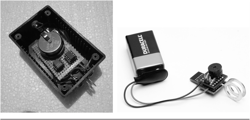
FIGURE 7-1 The ATtiny85 keyer (left) and the Digispark keyer (right).
The ATtiny85 is also produced by Atmel and has the feature set described in Table 7-1. As you can see, there is quite a bit of functionality crammed into an 8-pin DIP package. Given that our keyer design only requires three I/O lines, we can comfortably use an ATtiny85 for the keyer project.
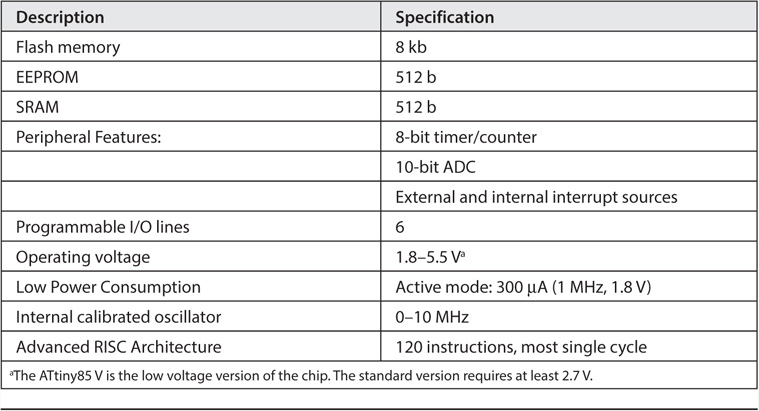
TABLE 7-1 ATtiny85 Feature Set
Actually, we are going to present two versions of the keyer to you in this chapter. The first version uses the ATtiny85 chip in its stand-alone DIP package. The second version uses the Digispark board produced by Digistump (http://digistump.com). See Figure 7-2 for pictures of the two versions of the ATtiny85 chip.

FIGURE 7-2 The Digispark chip on the left and the 8-pin ATtiny85 chip on the right. (Digispark courtesy of Digistump. ATtiny85 courtesy of cash)
The ATtiny85 chip can be purchased from domestic suppliers for about $2 each (see Appendix A). The Digispark board costs $9, but has a number of advantages. The biggest advantage is that funny-looking appendage sticking out of the left side of the Digispark board in Figure 7-2 is actually a USB connector. In other words, you can directly connect the Digispark board to your computer via a USB connection to program it. Not so with the barebones chip. To program the bare chip, we need to devise a simple circuit board and tie it to a 328-style Arduino board and use that board as the host programmer.
Required Software to Program an ATtiny85
You need to download and install certain libraries to be able to program the ATtiny85 chip. The “barebones” chip requires you to install the necessary files from the ATtiny-master.zip file, which can be found at https://github.com/damellis/attiny/. (The actual download button is near the lower-right side of the page.) The procedure you need to follow is a little different from what you would use for a “standard” library file, mainly because we need to alter the Arduino IDE in the process.
When you extract the zip file, you have a new directory named attiny-master created for you. Inside of that folder is another folder named attiny. That attiny folder needs to be copied to a new folder where your sketches are stored. You can use the File-Preferences menu option to see the location of your sketches folder, as shown in Figure 7-3.
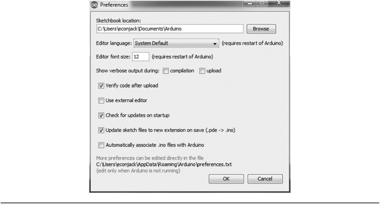
FIGURE 7-3 The preference menu option.
As you can see at the top of Figure 7-2, we installed the Arduino IDE so the sketches are saved at:
C:Arduino1.0.5Sketches.
Inside your sketches directory, create a new subdirectory named Hardware. (You may already have a Hardware directory. If so, ignore creating the new Hardware directory.) Now copy the attiny folder from the unzipped master directory into the hardware directory. For our system, the directory structure looks like:
C:Arduino1.0.5SketchesHardwareattiny
After you have copied the attiny directory, restart the Arduino IDE. Now, when you click on the Tools → Board option, you should see new options that cover the ATtiny chips. That is, your Board menu should now have new options that look like those shown in Figure 7-4. If you do not see the new options for the Board menu in the Arduino IDE, you need to redo the steps above. (You will also note that the Tools → Programmer menu option now has a USBtiny option, too.)
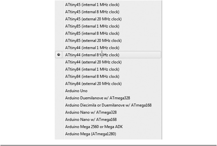
FIGURE 7-4 ATtinyXX board options.
Connecting the ATtiny85 to Your Arduino
You are now ready to build the circuit that is actually used to program the ATtiny85 chip. Figure 7-5 shows the pin assignments for the ATtiny85 chip. Notice that the labels for the pins are a little strange, in that what is labeled as circuit pin 0 is actually physical pin 5 on the chip. It’s very important not to confuse the physical pin position with the circuit pin position or you risk the chance of causing your ATtiny85’s untimely death. Figure 7-6 presents a breadboard view of the ATtiny85 programming shield.
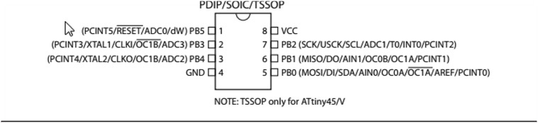
FIGURE 7-5 ATtiny85 pin assignments.

FIGURE 7-6 The layout of the ATtiny85 programming breadboard.
To help you prevent confusing physical and logical pin numbers, Table 7-2 gives you the ATtiny85 labels as well as the chip numbers. The table is based on Figure 7-6. The third column of the table tells you where each pin from the ATtiny85 chip (often called just ’85 in literature) is connected to your Arduino board. The fourth column relates to the ATmega1280 and ATmega2560 boards. So, for example, as you can see in Figure 7-6, the SCK line from the ATtiny85 runs from pin 7 of the ‘85 to pin 13 of the Arduino Uno. If you were using a Mega board, the SCK line would run to pin 52 on the Mega board. If you use Figure 7-6 in conjunction with Table 7-2, you should have no trouble wiring the shield.
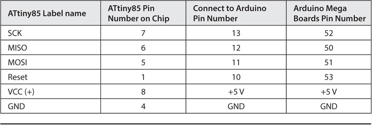
TABLE 7-2 Pin Assignments for ATtiny and Arduino Connecting Pins
Some Arduino boards aren’t happy unless you connect a 10 μF electrolytic capacitor between the RESET and GND pins on the Arduino board. Because this capacitor is polarized, make sure you connect the negative terminal to ground. Your connections should look similar to that shown in Figure 7-5.
Because we program ATtiny85 chips fairly often, we moved the breadboard circuit shown in Figure 7-6 to a “programming shield” that just piggybacks onto the Arduino board. (If you want more instructions on building an ATtiny85 programming shield, see: http://www.instructables.com/id/8-Pin-Programming-Shield/.) If this is the only ATtiny85 project you plan to build, the breadboard version is good enough. Figure 7-7 shows the shield we built for programming the ATtiny85.
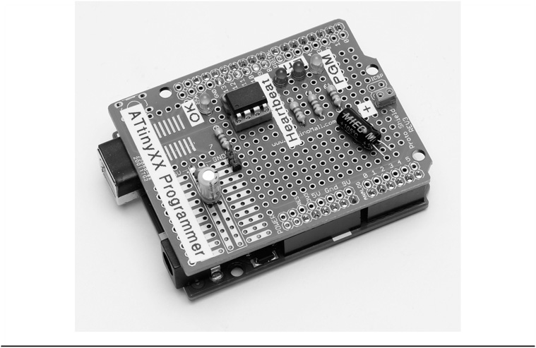
FIGURE 7-7 The programming shield for the ATtiny85 piggybacked to an Arduino.
The only thing about the shield is that we added two socket pins for the 10 μF capacitor. You can see the “+” mark labeled on the shield, near the right edge of the board. We did this because the capacitor needs to be removed when you load the ArduinoISP sketch, but must be replaced when you actually program the ATtiny85.
The Proper Programming Sequence
When you wish to program an ATtiny85 chip, there’s a specific sequence you must follow for everything to work properly. The following steps walk you through the sequence needed to program the ATtiny85:
1. Temporarily remove the 10 μF capacitor from the Arduino board.
2. If you have created a shield for the ATtiny85 programmer, plug it into the Uno or other 328-type Arduino board.
3. Load the ArduinoISP sketch found in the File → Examples directory.
4. Open “ArduinoISP” sketch from “Examples” folder.
5. Select your board from the Tools → Board menu. This should be the host Arduino board (e.g., Uno, Duemilanove).
6. Compile and upload the ArduinoISP sketch.
7. Replace the 10 μF capacitor and reinstall the programming shield (or the connections to the breadboard). Make sure you pay attention to its polarity.
8. From the Tools → Board menu, select the ATtiny85 (internal 8 MHz clock) option.
9. From the Tools → Programmer menu, select Arduino as ISP. (The ISP means the insystem programmer.)
10. At this point, you may want to upload the simple Blink program, change the program line that reads:
int led = 13;
to
int led = 0;
This is necessary because there is no pin 13 on the chip! Now connect a small LED between P0 (chip pin number 5) and the ground socket that holds the 10 μF capacitor. You should see the LED blink at a one second rate. This simply confirms that the program was successfully uploaded to the ATtiny85 chip.
11. You can now open the CW keyer sketch (presented later in this chapter) and compile it.
12. Upload the compiled sketch to the ATtiny85. For some host boards, you may see the messages:
avrdude: please define PAGEL and BS2 signals in the configuration
file for part ATtiny85
avrdude: please define PAGEL and BS2 signals in the configuration
file for part ATtiny85
You can ignore the error messages that refer to PAGEL or BS2 signals if they appear. Chances are good that the upload worked.
You should now remove the chip from its programming socket and place it in the circuit that uses the chip. It should work as you designed it. However, if things are not working correctly, the next section presents some potential areas where things may have gone wrong.
Some Things to Check If Things Go South
There are some issues that you need to be aware of in case your setup doesn’t correctly program the ATtiny85 chip. Consider the following checklist if you are having issues programming the chip using your Arduino:
1. Not all versions of the Atmel chip family are suitable for programming the ATtiny85. For example, the earlier ATmega168 won’t work. Also, we have purchased some 328s online that don’t work with the 1.0.5 IDE, but do work with the pre-1.0 IDE. While we are not sure, it seems that such boards have issues with the bootloader software that’s burned onto the chip. If you are unsure of your vendor’s board and its compatibility, ask if their board has been tested with version 1.0.5 of the IDE before you order the board.
2. Check the pin assignments in your program’s source code. It’s pretty easy to forget that you’re not working with a full Arduino board and to assume that you can still blink the LED on pin 13 when no pin 13 exists. While such flat-forehead mistakes do happen, usually they become obvious and no harm is done to the chip. Still, keep Figure 7-5 and Table 7-2 in mind when you move sketches from the Arduino to the ATtiny85.
3. Some versions of the Arduino IDE (e.g., version 1.0.2) simply don’t work when trying to program the ATtiny85. If you have an earlier version than 1.0.5, we suggest that you upgrade the Arduino IDE to the latest version.
4. Sometimes, having the circuit shown in Figure 7-6 connected to the Arduino board appears to prevent the sketch from properly loading into the Arduino. If that is the case, completely disconnect the ATtiny85 breadboard circuit from the Arduino board, load the sketch, and then reconnect the breadboard to the Arduino board. This is one reason that we created an “ATtiny85 programming shield” based on Figure 7-6. It’s a simple matter to remove the shield, load the sketch, and then plug the shield back into the Arduino board.
5. After programming the ATtiny85 chip, you may need to remove it from the programming circuit in order to make sure it is working properly. That is, testing the newly programmed chip in the circuit shown in Figure 7-6 may not work. It’s better to remove the chip from the programming socket and put it into the circuit in which you plan to use the chip for testing purposes.
6. The 10 μF capacitor that spans the RESET and GND pins on the Arduino board should be removed while loading the ArduinoISP sketch. However, be sure to put the capacitor back onto the board before trying to program the ATtiny85.
7. Keep in mind which pins on the ATtiny85 may be used as analog inputs (i.e., 3, 4, and 7).
At this point, you are ready to program the ATtiny85 with the code for the keyer. However, before we get to that code, we also want to show how to use the Digispark for the keyer.
Using the Digispark
The first thing you need to do is download a modified version of the Arduino IDE that is designed for use with the Digispark. This is a free download and can be found at:
http://sourceforge.net/projects/digistump/files/DigisparkArduino-Win32-1.0.4-May19.zip/download
NOTE: The Digispark IDE is a step or two behind the Arduino IDE in terms of version number, so make sure you keep the two IDEs in separate directories. Although the two IDEs look the same when they are run, they function differently under the hood, so don’t try to use the Arduino IDE to program the Digispark.
In Figure 7-8, you can see the +5 V and ground connections along the bottom of the board and the other pin connections (p) through P5, bottom to top along the right edge of the board. The USB connection is done via the connections on the left side of the board. If you are worried about the drain imposed on the battery by the LED, you can use a soldering iron to remove the LED (a little tricky because it is very small) or you can cut the traces using a sharp knife. Given the relatively small current drain for the LED, you could simply ignore the LED. Alternatively, you could add a switch to the circuit between the battery and the Digispark. We chose to ignore the LED’s current drain.
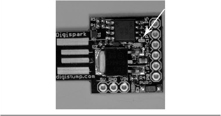
FIGURE 7-8 Close-up of the Digispark board with the onboard LED identified.
Table 7-3 shows the pinouts for the Digispark. All pins (P0 through P5) can be used for digital I/O.

TABLE 7-3 Digispark Pinouts Relative to ATtiny85
While it is true that the Digispark costs a little more than a naked ATtiny85 chip, there are a number of features that make the Digispark a worthy consideration. First, there is no need for the ISP setup used earlier in this chapter to program the ATtiny85. The Digispark has a USB port onboard that makes it work just like other Arduino boards. Second, it has an onboard voltage regulator that gives you more options in terms of powering the system. Although designed for 5 V operation (500 ma max), the regulator accepts up to 35 V at the ragged edge. (Digistump recommends not exceeding 12 V.) The regulator and USB chips do draw a little more current, but the board still has a decent battery life, especially if you use a 9 V battery. Third, the Digispark has an SMD LED similar to that on the Arduino Uno (see the arrow in Figure 7-8). Finally, the bootloader is already on the chip, which makes compiling and uploading programs very similar to the “normal” Arduino IDE.
Similar … yes. Identical … no.
Compiling and Uploading Programs with Digispark
When you start the Digispark IDE for the first time, you need to set the Tools → Board menu option to reflect that you are using a Digispark. Figure 7-9 shows the selection you should make. The topmost menu option is the correct one to select. (We truncated the list of options, as it is fairly long.) Also make sure the Tools → Programmer menu option is set to Digispark.

FIGURE 7-9 Board options (partial list) for Digispark.
You can now select a program to test the Digispark. Figure 7-10 shows the process for selecting the Digispark version of the Blink program found in the standard Arduino IDE. For the Digispark, the program is named Start. Note that you can also compile and run many of the standard Arduino examples, but you may have to make some minor changes. For example, the Blink program toggles the LED tied to pin 13 on the Arduino board. However, the Digispark doesn’t have a pin 13. Its LED pin is pin 1, so the code needs to be changed to reflect that fact. (The Start program includes the necessary source code change.) Pins 3 and 4 are used for USB communication when you are uploading a sketch to the Digispark. However, once the program is uploaded, those pins can resume their normal I/O functions.

FIGURE 7-10 Selecting the Start (Blink) program example.
After the Start program is loaded, you can click the “check mark” icon to compile the Start code. You should NOT click the compile-upload “right-arrow” icon.
At this point, you should unplug the Digispark from the USB cable. While this may seem a bit weird, it’s the way things work for the Digispark.
Once you see the Binary sketch size message as shown at the bottom of Figure 7-11, then you can click the “right-arrow” icon to upload the code. Note that the Digispark is still NOT connected to the USB cable at this time. (Interestingly, the Digispark compiles the Start program to 758 bytes, as can be seen in Figure 7-11. When you compile the Blink program using the standard Arduino 1.0.5 IDE, the program compiles to 1084 bytes. This suggests if you’re thinking you would like to move an Arduino sketch to the Digispark but are afraid it won’t fit, try compiling the Arduino code in the Digispark IDE and see what the final code size is. Also keep in mind that the Digispark library environment is not as robust as the Arduino libraries. However, more and more new Digispark libraries are coming online all the time.)

FIGURE 7-11 Compiling the Start program.
Figure 7-12 shows what happens when you click the upload icon. Note the message at the bottom of Figure 7-12. The IDE informs you that you have 60 seconds to plug the Digispark into the USB cable. If you don’t plug the Digispark into the USB cable within 60 seconds, you get a timeout message and the code is not uploaded. (On some boards, you may have to shut the IDE down and start over. On other boards, you just need to recompile and upload the source code.) When you plug the Digispark into the USB cable, you should see the green power LED come on. If you don’t see the green power LED come on, chances are you’ve put the Digispark into the connector upside down. Flip the Digispark over and try again.

FIGURE 7-12 The upload message from the Digispark IDE.
Assuming you do get the Digispark plugged into the USB cable in time, you will see messages giving you progress reports detailing the percentage of completion. You may also see progress messages telling you the IDE is erasing the old Digispark program along with upload messages. Finally, you should see:
>Starting the user app …
running: 100% complete
>> Micronucleus done. Thank you!
After the Digispark fission reactor shuts down (really?), you are ready to run the application that is now stored in the Digispark. You can disconnect the Digispark from the USB cable and place it in the circuit for which the software was written. For us, that is the CW keyer code, the subject of the next section.
Once you see the “Thank you” message, you know the program has been uploaded to the Digispark. It’s then possible to add a power source and whatever components you need and run your program. Figure 7-13 shows the Digispark after uploading the keyer code and adding a battery plus two wires that serve to test the keying. As you can see in Figure 7-13, the battery (a CR2477) and its holder are about the same size as the Digispark. The CR2477 is rated at 1000 mAh, which, given the small current drain of the Digispark, should have the shelf life of granite even without a power switch. Another good battery choice is a standard 9 V battery, as shown in Figure 7-1. The two wires leading toward the bottom of the picture are attached to the keying paddles. You can actually test the circuit by just touching the wires.

FIGURE 7-13 Prototype CW keyer using the Digispark.
The CW Keyer
Testing the prototype using the hardware shown in Figure 7-13 is pretty easy. There is very little to the circuit. The final circuit, however, may have an on-off switch. The reason we say “may have an on-off switch” is because it may not be worth it, especially if you are using the ATtiny85 by itself. With the bare chip drawing about 300 μA, the CR2477 should last over 2000 hours. The Digispark, however, has an onboard voltage regulator and power LED that increases the battery draw. Still, even assuming the worst-case assumptions about the additional current draw, the Digispark should provide at least 400 hours of operation on a single 9 V battery.
So, why all the fuss about a switch? After all, the switch only costs a buck or two, so why not include it? Actually, it’s not the cost of the switch that is an issue to us, it’s the “added appendage” that we object to. That is, we want a keyer with minimal moving parts, that is rugged, and doesn’t have “stuff” sticking out that can break off in the field. Not using a switch is one less thingy sticking out of the case that can break in the field. Also, you can always remove the battery from its holder.
Adjusting Code Speed
Some of us are not the fastest fist in the West and appreciate it when an operator realizes we’re struggling and QRS’s for our benefit. Having the ability to adjust the keyer speed is a nice feature. Of course, you could have a small pot that is adjustable via a small screwdriver through a hole in the keyer case and use the chip’s ADC capabilities to alter the speed. However, that’s the beauty of a μC: we can set the speed in software. Simply stated, the program’s source code recognizes that, if you hold the “dah key” for 10 consecutive strobes (i.e., greater than DAHTRIGGER), it lowers the keyer speed by approximately 1 word per minute. If you hold the “dit key” for 10 consecutive strobes (DITTRIGGER), it increases the keyer speed by 1 word per minute. (You can change the symbolic constants for the strobe counts to whatever makes sense to you.) Using a software approach to speed change makes it easy to change the code speed without having to use a potentiometer in the circuit. Not using a potentiometer also keeps the cost down and lowers the space requirements. If you don’t like the way we have implemented the speed changing method, you can either change the circuit or the software to suit your needs.
Capacitance Sensors
The Arduino family of μCs are capable of making a touch-sensitive input using any of the Arduino pins. As you saw in Figure 7-13, two plain wires were used to make the keyer paddles for the prototype of the CW keyer. All you have to do is set the pin being used as the sensor to ground, turn on the chip’s pull-up resistor, and measure how long it takes the pin to change state.
A number of programmers have refined a function, readCapacitivePin(), that is designed to return a value between 0 and 17 depending upon the level of capacitance on the pin. You can read the background information at http://playground.arduino.cc/Code/CapacitiveSensor. That reference points out that, although no hardware is required to make the touch sensor, a 1 nF capacitor in line with the pin being used helps reduce noise on the line. We chose to omit those caps because the keyer works fine without them. The authors also warn not to connect any voltage source to the sensor pin as it could damage the μC chip. Although not required for most modern rigs, we have added a 4N26 optoisolator to the keying circuit in much the same way it is used in Chapter 9 (see Figure 9-5).
The CW keyer source code is presented in Listing 7-1. The code begins with a series of #defines. The #define DEBUG preprocessor directive is used primarily to toggle the digitalWrite() method calls on the LED in and out of the program. This makes it easier to see what the code is doing and debug the program as needed. Obviously, you want the debug code removed when you are ready to program the chip for use in your circuit, so comment out the #define DEBUG directive at that time. The directives for DAHPADDLEPIN and DITPADDLEPIN are somewhat arbitrary since any digital pin can be used as a sensor. However, pin 1 on the Digispark is used for the onboard LED, which we do use in the debug mode, so we don’t use it for one of the touch sensors. The OUTPUTPIN is the actual keying line and its output is fed into the 4N26 optoisolator. Figure 7-14 shows the complete schematic for the keyer using the ATtiny85 chip. The Digispark is essentially the same, but uses a 9 V battery.
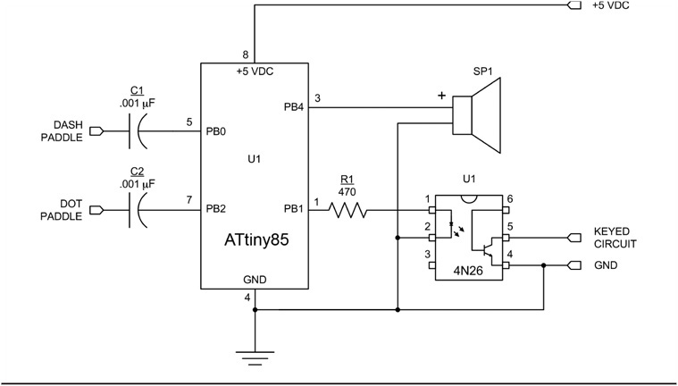
FIGURE 7-14 Schematic for ATtiny85 keyer.


LISTING 7-1 The CW keyer using touch sensors.
The #define MYTRIGGERVALUE is one preprocessor directive value with which you may have to experiment. A whole host of factors can affect the actual behavior of the capacitance being placed on a sensor pin. Everything from the circuit ground to the size of the paddle sensor can affect the values being read. It is even possible to sense body capacitance without touching the sensor. We suggest you try the code starting with the value of 1 for this directive and see how the circuit behaves. In our initial tests, when the “paddles” were nothing more than wires connected to the pins, the value 1 worked fine. However, when we tried it with a large double-sided copper clad circuit board as the “paddle,” we could actually trigger the circuit without touching it using the value of 1 for the threshold value.
In the setup() function, some debug code (which you’ve seen before) is run and then we set OUTPUTPIN to the output mode using a call to pinMode(). The default keyer speed is set to 13 words per minute (i.e., 65 characters per minute). Using the standard timing formula, a dit then corresponds to about 92 ms. A dah is then fixed to three times that time period. The inter-atom spacing is assumed to be one dit. That is, the letter “S” is 92 ms (dit), 92 ms (atom space), 92 ms (dit), 92 ms (atom space), 92 ms (dit), 92 ms (atom space). This means that every completed letter is automatically followed by one atom space. Obviously, final letter and word spacing is determined by the operator.
If you follow the comments for DITADJUST, you’ll discover that changing the words per minute means that the dit speed in milliseconds rises (for a slower speed) or falls (for a faster speed) by 7 ms each time DITADJUST is changed. TOPSPEED and SLOWSPEED are used to set the maximum and minimum words per minute speeds.
The volatile Keyword
The loop() function first call the readCapacitivePin() for the DAHPADDLEPIN. Note the use of the volatile keyword for the first three variables used in the function. You use the volatile keyword to force the compiler to reload the rvalue of the variable each time it is referenced. Optimizing compilers often cache the rvalue of a variable, keeping it in a central processing unit (CPU) register to improve execution speed. However, if external resources can alter the value, it is possible to have the program be “out of sync” with the actual value for the variable. Using the volatile keyword forces the compiler to reload the most current value of the variable.
To get the most accurate reading from the pin as possible, the readCapacitivePin() code disables, interrupts, and then unrolls the polling of the pin using pointers to minimize the number of machine cycles required to read the pin. When the pin transitions, the value (0 to 17) is returned to the caller. If the return value stored in dahCycles is greater than MYTRIGGERVALUE, the sendDah() function is called. The same process is repeated for the dit sensor. Therefore, all the loop() function does is continually scan the dit and dah sensors looking for a change in capacitance. When that happens, the appropriate function is called to send a dit or a dah.
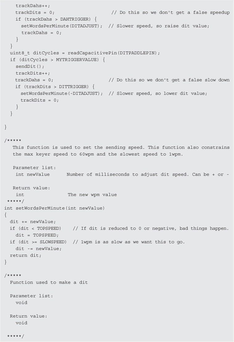
The setWordsPerMinute() function is used to change the sending speed. Two variables, trackDits and trackDahs, store the sequence of dits and dahs that have been sensed. The longest Morse sequence using dits is the number 5, comprised of five dits. The longest sequence using dahs is the number 0, comprised of five dahs. The symbolic constants DAHTRIGGER and DITTRIGGER are defined as 9. This means that 10 consecutive dits raise the word per minute (wpm) by one. Likewise, 10 consecutive dahs lower the words per minute by one. These conventions make it fairly easy to adjust the code speed for the keyer.
Construction
The actual construction method you use is determined by which version of the keyer you plan to build. Let’s build the ATtiny85 versions first. Figure 7-15 shows what our keyer looks like. You can use just about any case you wish as long as it’s big enough to hold the components. (The case here was from Jameco Electronics, approximately 3 × 2 × 1.25 in. in size.) On the right side of the keyer in Figure 7-13, you can see the two small metal corner braces that we use for the dit and dah paddle levers. The ATtiny85 is the 8-pin chip on the top of the perf board and the 4N26 optoisolator is the 6-pin chip just below it. The battery is a CR2477, which provides 3 V for the keyer and is rated at 1 AHr. The ATtiny85 can operate with as little as 2.5 V, so the CR2477 supplies enough voltage for the chip. (The battery would not supply sufficient voltage for the Digispark, however, in part because of the onboard voltage regulator and LED.)
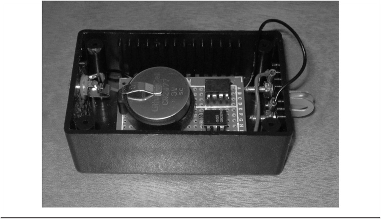
FIGURE 7-15 The ATtiny85 keyer. (Case courtesy of Jameco)
The output from the optoisolator is tied to the standard audio jack on the left edge of the case. You could leave this out and simply pass a wire through the case to a plug that is compatible with your rig. However, we have rigs that use both a ¼ in. and ⅛ in. jacks. Depending upon which rig we want to use, we have made a pair of connecting cables, one terminated with a ¼ in. plug and the other terminated with a ⅛ in. plug on one end and ⅛ in. plugs on the other ends. This approach means we don’t have a loose plug wire dangling from the keyer when it’s not in use. Pick whatever wiring best suits your needs.
We simply hot glued the perf board to the plastic case. While we can imagine that prying the battery from its holder may prove a little bit difficult, even with no power switch, we have yet to drain the battery. Some back-of-the-napkin calculations suggest that the battery should provide power for several thousand hours even when left on continuously. Of course, you could simply remove the battery if you plan to leave it idle for any length of time.
Figure 7-16 presents another perspective of the Digispark version of the keyer that Dennis built. The glow emanating from the bottom of the keyer is from the Digispark onboard LED. Dennis also included a small buzzer, which you can see atop the small prototyping board available from Digistump. Dennis has his keyer tied to the Palm Paddle set of commercial paddles. He also has the Digispark version shown in Figure 7-1.
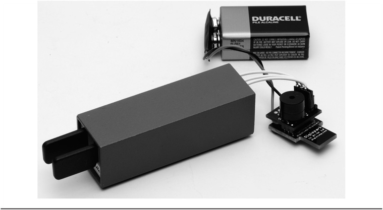
FIGURE 7-16 The Digispark version of the keyer.
The parts Dennis used to construct the Digispark keyer shown in Figure 7-16 are presented in Figure 7-17. The parts show the two 1 nF capacitors that you might need to insert into the paddle leads under certain noisy conditions. The header pins are used to tie the prototype board to the Digispark.
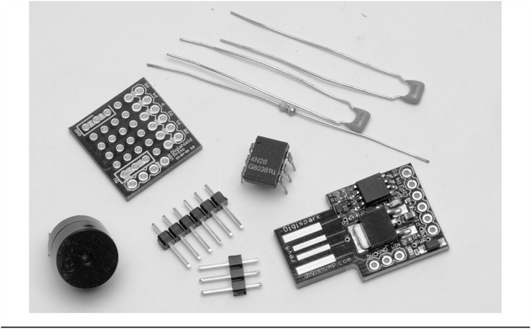
FIGURE 7-17 Digispark keyer parts.
Figure 7-18 presents a parts placement for the components shown in Figure 7-17. One advantage of Dennis’s design is that the buzzer serves as a side tone for many low-cost QRP rigs that don’t provide a sidetone.
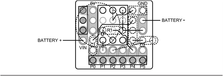
FIGURE 7-18 Parts placement for Digispark prototype board.
Conclusion
This chapter has presented two designs for a simple keyer. Perhaps equally important, however, is that you learned how to build and program a μC circuit using the ATtiny85 chip. Such an approach is useful when the demands of your project don’t warrant the expense of a full Arduino board. Knowing how to program the ATtiny85 gives you another tool to hang on your tool belt, and that’s a good thing. After all, if the only tool you have is a hammer, all of your problems start to look like a nail.
Keep in mind that the ATtiny85 still has lots of program space left if you care to add new features to the keyer. You could, for example, hard code some messages (e.g., CQ, CQ, CQ DE…) into the chip and devise a way to activate those when needed. If you do add new features to the keyer, we hope you’ll share your efforts with the rest of us via the web site.