
Chapter 10. Audio Amplifier Performance
10.1. A Brief History of Amplifiers
A full and detailed account of semiconductor amplifier design since its beginnings would be a book in itself, and a most fascinating volume it would be. This is not that book, but I still feel obliged to give a very brief account of how amplifier design has evolved in the last three or four decades.
Valve amplifiers, working in push–pull Class-A or AB1, and perforce transformer coupled to the load, were dominant until the early 1960s, when truly dependable transistors could be made at a reasonable price. Designs using germanium devices appeared first, but suffered severely from the vulnerability of germanium to even moderately high temperatures; the term thermal runaway was born. At first all silicon power transistors were NPN, and for a time most transistor amplifiers relied on input and output transformers for push–pull operation of the power output stage. These transformers were as always heavy, bulky, expensive, and nonlinear and added insult to injury as their LF and HF phase shifts severely limited the amount of negative feedback (NFB) that could be applied safely.
The advent of the transformerless Lin configuration,[1] with what became known as a quasi-complementary output stage, disposed of a good many problems. Because modestly capable PNP driver transistors were available, the power output devices could both be NPN and still work in push–pull. It was realized that a transformer was not required for impedance matching between power transistors and 8-Ω loudspeakers.
Proper complementary power devices appeared in the late 1960s, and full complementary output stages soon proved to give less distortion than their quasi-complementary predecessors. At about the same time, DC-coupled amplifiers began to take over from capacitor-coupled designs, as the transistor differential pair became a more familiar circuit element.
A much fuller and generally excellent history of power amplifier technology is given in Sweeney and Mantz.[2]
10.2. Amplifier Architectures
This grandiose title simply refers to the large-scale structure of the amplifier, that is, the block diagram of the circuit one level below that representing it as a single white block-labeled power amplifier. Almost all solid-state amplifiers have a three-stage architecture as described here, although they vary in the detail of each stage.
10.3. The Three-Stage Architecture
The vast majority of audio amplifiers use the conventional architecture, shown in Figure 10.1. There are three stages, the first being a transconductance stage (differential voltage in, current out), the second a transimpedance stage (current in, voltage out), and the third a unity-voltage-gain output stage. The second stage clearly has to provide all the voltage gain and I have therefore called it the voltage-amplifier stage or VAS. Other authors have called it the predriver stage but I prefer to reserve this term for the first transistors in output triples. This three-stage architecture has several advantages, not least being that it is easy to arrange things so that the interaction between stages is negligible. For example, there is very little signal voltage at the input to the second stage due to its current input (virtual-earth) nature, and therefore very little on the first stage output; this minimizes Miller phase shift and possible early effect in the input devices.
Figure 10.1. The three-stage amplifier structure. There is a transconductance stage, a transadmittance stage (the VAS), and a unity-gain buffer output stage.

Similarly, the compensation capacitor reduces the second stage output impedance so that the nonlinear loading on it due to the input impedance of the third stage generates less distortion than might be expected. The conventional three-stage structure, familiar though it may be, holds several elegant mechanisms such as this. Since the amount of linearizing global NFB available depends on amplifier open-loop gain, how the stages contribute to this is of great interest. The three-stage architecture always has a unity-gain output stage—unless you really want to make life difficult for yourself—and so the total forward gain is simply the product of the transconductance of the input stage and the transimpedance of the VAS, the latter being determined solely by the Miller capacitor Cdom, except at very low frequencies. Typically, the closed-loop gain will be between+20 and+30 dB. The NFB factor at 20 kHz will be 25 to 40 dB, increasing at 6 dB per octave with falling frequency until it reaches the dominant pole frequency P1, when it flattens out. What matters for the control of distortion is the amount of NFB available, rather than the open-loop bandwidth, to which it has no direct relationship. In my Electronics World Class-B design, the input stage gm is about 9 mA/V, and Cdom is 100 pF, giving an NFB factor of 31 dB at 20 kHz. In other designs I have used as little as 26 dB (at 20 kHz) with good results.
Compensating a three-stage amplifier is relatively simple; since the pole at the VAS is already dominant, it can be easily increased to lower the HF NFB factor to a safe level. The local NFB working on the VAS through Cdom has an extremely valuable linearizing effect.
The conventional three-stage structure represents at least 99% of the solid-state amplifiers built, and I make no apology for devoting much of this book to its behavior. I doubt if I have exhausted its subtleties.
10.3.1. Two-Stage Amplifier Architecture
In contrast, the architecture shown in Figure 10.2 is a two-stage amplifier, with the first stage once again being more a transconductance stage, although now without a guaranteed low impedance to accept its output current. The second stage combines VAS and output stage in one block; it is inherent in this scheme that the VAS must double as a phase splitter as well as a generator of raw gain. There are then two quite dissimilar signal paths to the output, and it is not at all clear that trying to break this block down further will assist a linearity analysis. The use of a phase-splitting stage harks back to valve amplifiers; where it was inescapable as a complementary valve technology has, so far, eluded us.
Figure 10.2. The two-stage amplifier structure. A voltage-amplifier output follows the same transconductance input stage.

Paradoxically, a two-stage amplifier is likely to be more complex in its gain structure than a three stage. The forward gain depends on the input stage gm, the input stage collector load (because the input stage can no longer be assumed to be feeding a virtual earth), and the gain of the output stage, which will be found to vary in a most unsettling manner with bias and loading. Choosing the compensation is also more complex for a two-stage amplifier, as the VAS/phase splitter has a significant signal voltage on its input and so the usual pole-splitting mechanism that enhances Nyquist stability by increasing the pole frequency associated with the input stage collector will no longer work so well. (I have used the term Nyquist stability or Nyquist oscillation throughout this book to denote oscillation due to the accumulation of phase shift in a global NFB loop, as opposed to local parasitics, etc.)
The LF feedback factor is likely to be about 6 dB less with a 4-Ω load due to lower gain in the output stage. However, this variation is much reduced above the dominant pole frequency, as there is then increasing local NFB acting in the output stage.
Two-stage amplifiers are not popular; I can quote only two examples, Randi[3]and Harris.[4]The two-stage amplifier offers little or no reduction in parts cost, is harder to design, and, in my experience, invariably gives a poor distortion performance.
10.4. Power Amplifier Classes
For a long time the only amplifier classes relevant to high-quality audio were Class-A and Class-AB. This is because valves were the only active devices, and Class-B valve amplifiers generated so much distortion that they were barely acceptable, even for public address purposes. All amplifiers with pretensions to high fidelity operated in push–pull Class-A.
Solid state gives much more freedom of design; all of the following amplifier classes have been exploited commercially. Unfortunately, there will only be space to deal in detail in this book with A, AB, and B, although this certainly covers the vast majority of solid-state amplifiers. Plentiful references are given so that the intrigued can pursue matters further.
10.4.1. Class-A
In a Class-A amplifier, current flows continuously in all the output devices, which enables the nonlinearities of turning them on and off to be avoided. They come in two rather different kinds, although this is rarely explicitly stated, which work in very different ways. The first kind is simply a Class-B stage (i.e., two emitter–followers working back to back) with the bias voltage increased so that sufficient current flows for neither device to cut off under normal loading. The great advantage of this approach is that it cannot abruptly run out of output current; if the load impedance becomes lower than specified, then the amplifier simply takes brief excursions into Class-AB, hopefully with a modest increase in distortion and no seriously audible distress.
The other kind could be called a controlled-current source type, which is, in essence, a single emitter–follower with an active emitter load for adequate current sinking. If this latter element runs out of current capability, it makes the output stage clip much as if it had run out of output voltage. This kind of output stage demands a very clear idea of how low an impedance it will be asked to drive before design begins.
Valve textbooks contain enigmatic references to classes of operation called AB1 and AB2; in the former, grid current did not flow for any part of the cycle, but in the latter, it did. This distinction was important because the flow of output-valve grid current in AB2 made the design of the previous stage much more difficult.
AB1 or AB2 has no relevance to semiconductors, for base current in BJT always flows when a device is conducting, whereas gate current in power FET never does, apart from charging and discharging internal capacitances.
10.4.2. Class-AB
This is not really a separate class of its own, but a combination of A and B. If an amplifier is biased into Class-B and then the bias increased further, it will enter AB. For outputs below a certain level, both output devices conduct and operation is Class-A. At higher levels, one device will be turned completely off as the other provides more current, and the distortion jumps upward at this point as AB action begins. Each device will conduct between 50 and 100% of the time, depending on the degree of excess bias and the output level.
Class-AB is less linear than either A or B, and in my view its only legitimate use is as a fallback mode to allow Class-A amplifiers to continue working reasonably when faced with low-load impedance.
10.4.3. Class-B
Class-B is by far the most popular mode of operation, and probably more than 99% of the amplifiers currently made are of this type. Most of this book is devoted to it, so no more is said here.
10.4.4. Class-C
Class-C implies device conduction for significantly less than 50% of the time and is normally only usable in radio work, where an LC circuit can smooth out the current pulses and filters harmonics. Current-dumping amplifiers can be regarded as combining Class-A (the correcting amplifier) with Class-C (the current-dumping devices); however, it is hard to visualize how an audio amplifier using devices in Class-C only could be built.
10.4.5. Class-D
These amplifiers continuously switch the output from one rail to the other at a supersonic frequency, controlling the mark/space ratio to give an average representing the instantaneous level of the audio signal; this is alternatively called pulse width modulation. Great effort and ingenuity have been devoted to this approach, for the efficiency is, in theory, very high, but the practical difficulties are severe, especially so in a world of tightening EMC legislation, where it is not at all clear that a 200-kHz high-power square wave is a good place to start. Distortion is not inherently low[5]and the amount of global NFB that can be applied is severely limited by the pole due to the effective sampling frequency in the forward path. A sharp cutoff low-pass filter is needed between amplifier and speaker to remove most of the RF; this will require at least four inductors (for stereo) and will cost money, but its worst feature is that it will only give a flat frequency response into one specific load impedance. The technique now has a whole chapter of this book to itself. Other references to consult for further information are Goldberg and Sandler[6] and Hancock.[7]
10.4.6. Class-E
An extremely ingenious way to operate a transistor is to have either a small voltage across it or a small current through it almost all the time; in other words, the power dissipation is kept very low.[8] Regrettably, this is an RF technique that seems to have no sane application to audio.
10.4.7. Class-F
There is no Class-F, as far as I know. This seems like a gap that needs filling.
10.4.8. Class-G
This concept was introduced by Hitachi in 1976 with the aim of reducing amplifier power dissipation. Musical signals have a high peak/mean ratio, spending most of this at low levels, so internal dissipation is much reduced by running from low-voltage rails for small outputs, switching to higher rails current for larger excursions.
The basic series Class-G with two rail voltages (i.e., four supply rails, as both voltage are ±) is shown in Figure 10.3.[9,11] Current is drawn from the lower ±V1 supply rails whenever possible; should the signal exceed ±V1, TR6 conducts and D3 turns off, so the output current is now drawn entirely from the higher ±V2 rails, with power dissipation shared between TR3 and TR6. The inner stage TR3, TR4 is usually operated in Class-B, although AB or A is equally feasible if the output stage bias is suitably increased. The outer devices are effectively in Class-C as they conduct for significantly less than 50% of the time.
Figure 10.3. Class-G-series output stage. When the output voltage exceeds the transition level, D3 or D4 turn off and power is drawn from the higher rails through the outer power devices.
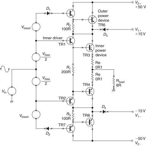
In principle, movements of the collector voltage on the inner device collectors should not significantly affect the output voltage, but in practice, Class-G is often considered to have poorer linearity than Class-B because of glitching due to charge storage in commutation diodes D3, D4. However, if glitches occur they do so at moderate power, well displaced from the crossover region, and so appear relatively infrequently with real signals.
An obvious extension of the Class-G principle is to increase the number of supply voltages. Typically the limit is three. Power dissipation is further reduced and efficiency increased as the average voltage from which the output current is drawn is kept closer to the minimum. The inner devices operate in Class-B/AB as before, and the middle devices are in Class-C. The outer devices are also in Class-C, but conduct for even less of the time.
To the best of my knowledge, three-level Class-G amplifiers have only been made in shunt mode, as described later, probably because in series mode the cumulative voltage drops become too great and compromise the efficiency gains. The extra complexity is significant, as there are now six supply rails and at least six power devices, all of which must carry the full output current. It seems most unlikely that this further reduction in power consumption could ever be worthwhile for domestic hi-fi.
A closely related type of amplifier is Class-G shunt.[10]Figure 10.4 shows the principle; at low outputs, only Q3, Q4 conduct, delivering power from the low-voltage rails. Above a threshold set by Vbias3 and Vbias4, D1 or D2 conduct and Q6, Q8 turn on, drawing current from the high-voltage rails, with D3, 4 protecting Q3, 4 against reverse bias. The conduction periods of the Q6, Q8 Class-C devices are variable, but inherently less than 50%. Normally the low-voltage section runs in Class-B to minimize dissipation. Such shunt Class-G arrangements are often called “commutating amplifiers.”
Figure 10.4. A Class-G shunt output stage, composed of two EF output stages with the usual drivers. Vbias3,4 set the output level at which power is drawn from the higher rails.

Some of the more powerful Class-G shunt PA amplifiers have three sets of supply rails to further reduce the average voltage drop between rail and output. This is very useful in large PA amplifiers.
10.4.9. Class-H
Class-H is once more basically Class-B, but with a method of dynamically boosting the single supply rail (as opposed to switching to another one) in order to increase efficiency.[12] The usual mechanism is a form of bootstrapping. Class-H is used occasionally to describe Class-G as described earlier; this sort of confusion we can do without.
10.4.10. Class-S
Class-S, so named by Doctor Sandman,[13] uses a Class-A stage with very limited current capability, backed up by a Class-B stage connected so as to make the load appear as a higher resistance that is within the capability of the first amplifier.
The method used by the Technics SE-A100 amplifier is extremely similar.[14] I hope that that this necessarily brief catalogue is comprehensive; if anyone knows of other bona fide classes I would be glad to add them to the collection. This classification does not allow a completely consistent nomenclature; for example, quad-style current dumping can only be specified as a mixture of Class-A and -C, which says nothing about the basic principle of operation, which is error correction.
10.4.11. Variations on Class-B
The solid-state Class-B three-stage amplifier has proved both successful and flexible, so many attempts have been made to improve it further, usually by trying to combine the efficiency of Class-B with the linearity of Class-A. It would be impossible to give a comprehensive list of the changes and improvements attempted, so I give only those that have been either commercially successful or particularly thought provoking to the amplifier-design community.
10.4.12. Error-Correcting Amplifiers
This refers to error-cancellation strategies rather than the conventional use of NFB. This is a complex field, for there are at least three different forms of error correction, of which the best known is error feedforward as exemplified by the ground-breaking Quad 405.[15] Other versions include error feedback and other even more confusingly named techniques, some of which turn out on analysis to be conventional NFB in disguise. For a highly ingenious treatment of the feedforward method, see Giovanni Stochino.[16]
10.4.13. Nonswitching Amplifiers
Most of the distortion in Class-B is crossover distortion and results from gain changes in the output stage as the power devices turn on and off. Several researchers have attempted to avoid this by ensuring that each device is clamped to pass a certain minimum current at all times.[17] This approach has certainly been exploited commercially, but few technical details have been published. It is not intuitively obvious (to me, anyway) that stopping the diminishing device current in its tracks will give less crossover distortion.
10.4.14. Current-Drive Amplifiers
Almost all power amplifiers aspire to be voltage sources of zero output impedance. This minimizes frequency response variations caused by the peaks and dips of the impedance curve and gives a universal amplifier that can drive any loudspeaker directly.
The opposite approach is an amplifier with a sufficiently high output impedance to act as a constant-current source. This eliminates some problems, such as rising voice-coil resistance with heat dissipation, but introduces others, such as control of the cone resonance. Current amplifiers therefore appear to be only of use with active crossovers and velocity feedback from the cone.[18]
It is relatively simple to design an amplifier with any desired output impedance (even a negative one) and so any compromise between voltage and current drive is attainable. The snag is that loudspeakers are universally designed to be driven by voltage sources, and higher amplifier impedances demand tailoring to specific speaker types.[19]
10.4.15. The Blomley Principle
The goal of preventing output transistors from turning off completely was introduced by Peter Blomley in 1971[20]; here the positive/negative splitting is done by circuitry ahead of the output stage, which can then be designed so that a minimum idling current can be separately set up in each output device. However, to the best of my knowledge this approach has not yet achieved commercial exploitation.
10.4.16. Geometric Mean Class-AB
The classical explanations of Class-B operation assume that there is a fairly sharp transfer of control of the output voltage between the two output devices, stemming from an equally abrupt switch in conduction from one to the other. In practical audio amplifier stages this is indeed the case, but it is not an inescapable result of the basic principle. Figure 10.5 shows a conventional output stage, with emitter resistors Re1, Re2 included to increase quiescent-current stability and allow current sensing for overload protection; to a large extent, these emitter resistances make classical Class-B what it is.
Figure 10.5. A conventional double emitter–follower output stage with emitter resistors Re shown.

However, if the emitter resistors are omitted and the stage biased with two matched diode junctions, then the diode and transistor junctions form a translinear loop[21] around which the junction voltages sum to zero. This links the two output transistor currents Ip, In in the relationship In * Ip=constant, which in op-amp practice is known as geometric-mean Class-AB operation. This gives smoother changes in device current at the crossover point, but this does not necessarily mean lower THD. Such techniques are not very practical for discrete power amplifiers; first, in the absence of the very tight thermal coupling between the four junctions that exists in an IC, the quiescent-current stability will be atrocious, with thermal runaway and spontaneous combustion a near certainty. Second, the output device bulk emitter resistance will probably give enough voltage drop to turn the other device off anyway, when current flows. The need for drivers, with their extra junction drops, also complicates things.
A new extension of this technique is to redesign the translinear loop so that 1/In+1/Ip=constant; this is known as harmonic-mean AB operation.[22] It is too early to say whether this technique (assuming it can be made to work outside an IC) will be of use in reducing crossover distortion and thus improving amplifier performance.
10.4.17. Nested Differentiating Feedback Loops
This is a most ingenious, but conceptually complex technique for significantly increasing the amount of NFB that can be applied to an amplifier (see Cherry[23]).
10.5. AC- and DC-Coupled Amplifiers
All power amplifiers are either AC coupled or DC coupled. The first kind have a single supply rail, with the output biased to be halfway between this rail and ground to give the maximum symmetrical voltage swing; a large DC-blocking capacitor is therefore used in series with the output. The second kind have positive and negative supply rails, and the output is biased to be at 0 V, so no output DC blocking is required in normal operation.
10.5.1. Advantages of AC Coupling
- The output DC offset is always zero (unless the output capacitor is leaky).
- It is very simple to prevent turn-on thump by purely electronic means. The amplifier output must rise up to half the supply voltage at turn on, but providing this occurs slowly, there is no audible transient. Note that in many designs, this is not simply a matter of making the input bias voltage rise slowly, as it also takes time for the DC feedback to establish itself, and it tends to do this with a snap action when a threshold is reached.
- No protection against DC faults is required, providing that the output capacitor is voltage rated to withstand the full supply rail. A DC-coupled amplifier requires an expensive and possibly unreliable output relay for dependable speaker protection.
- The amplifier should be easier to make short-circuit proof, as the output capacitor limits the amount of electric charge that can be transferred each cycle, no matter how low the load impedance. This is speculative; I have no data as to how much it really helps in practice.
- AC-coupled amplifiers do not, in general, appear to require output inductors for stability. Large electrolytics have significant equivalent series resistance (ESR) and a little series inductance. For typical amplifier output sizes the ESR will be of the order of 100 mΩ; this resistance is probably the reason why AC-coupled amplifiers rarely had output inductors, as it is enough resistance to provide isolation from capacitative loading and so gives stability. Capacitor series inductance is very low and probably irrelevant, being quoted by one manufacturer as a few tens of nanoHenrys’. The output capacitor was often condemned in the past for reducing the low-frequency damping factor (DF), for its ESR alone is usually enough to limit the DF to 80 or so. As explained earlier, this is not a technical problem because “damping factor” means virtually nothing.
10.5.2. Advantages of DC Coupling
- No large and expensive DC-blocking capacitor is required. However, the dual supply will need at least one more equally expensive reservoir capacitor and a few extra components such as fuses.
- In principle, there should be no turn-on thump, as the symmetrical supply rails mean the output voltage does not have to move through half the supply voltage to reach its bias point—it can just stay where it is. In practice, the various filtering time constants used to keep the bias voltages free from ripple are likely to make various sections of the amplifier turn on at different times, and the resulting thump can be substantial. This can be dealt with almost for free, when a protection relay is fitted, by delaying the relay pull-in until any transients are over. The delay required is usually less than a second.
- Audio is a field where almost any technical eccentricity is permissible, so it is remarkable that AC coupling appears to be the one technique that is widely regarded as unfashionable and unacceptable. DC coupling avoids any marketing difficulties.
- Some potential customers will be convinced that DC-coupled amplifiers give better speaker damping due to the absence of output capacitor impedance. They will be wrong, as explained later, but this misconception has lasted at least 40 years and shows no sign of fading away.
- Distortion generated by an output capacitor is avoided. This is a serious problem, as it is not confined to low frequencies,
as is the case in small-signal circuitry. For a 6800-μF output capacitor driving 4 W into an 8-Ω load, there is significant
midband third harmonic distortion at 0.0025%, as shown in Figure 10.6. This is at least five times more than the amplifier generates in this part of the frequency range. In addition, the THD
rise at the LF end is much steeper than in the small-signal case, for reasons that are not yet clear. There are two cures
for output capacitor distortion. The straightforward approach uses a huge output capacitor, far larger in value than required
for a good low-frequency response. A 100,000-μF/40-V Aerovox from BHC eliminated all distortion, as shown in Figure 10.7. An allegedly “audiophile” capacitor gives some interesting results; a Cerafine Supercap of only moderate size (4700 μF/63
V) gave Figure 10.8, where the midband distortion is gone, but the LF distortion rise remains. What special audio properties this component is
supposed to have are unknown; as far as I know, electrolytics are never advertised as low midband THD, but that seems to be
the case here. The volume of the capacitor case is about twice as great as conventional electrolytics of the same value, so
it is possible the crucial difference may be a thicker dielectric film than is usual for this voltage rating.
Figure 10.6. The extra distortion generated by an 6800-μF electrolytic delivering 40 W into 8 Ω. Distortion rises as frequency falls, as for the small-signal case, but at this current level there is also added distortion in the midband.

Figure 10.7. Distortion with and without a very large output capacitor, the BHC Aerovox 100,000 μF/40 V (40 watts/8 Ω). Capacitor distortion is eliminated.

Figure 10.8. Distortion with and without an “audiophile” Cerafine 4700-μF/63-V capacitor. Midband distortion is eliminated but LF rise is much the same as the standard electrolytic.

Either of these special capacitors costs more than the rest of the amplifier electronics put together. Their physical size is large. A DC-coupled amplifier with protective output relay will be a more economical option.
A little-known complication with output capacitors is that their series reactance increases the power dissipation in the output stage at low frequencies. This is counterintuitive as it would seem that any impedance added in series must reduce the current drawn and hence the power dissipation. In fact, it is the load phase shift that increases the amplifier dissipation.
- The supply currents can be kept out of the ground system. A single-rail AC amplifier has half-wave Class-B currents flowing in the 0-V rail, which can have a serious effect on distortion and cross talk performance.
10.6. Negative Feedback in Power Amplifiers
It is not the role of this book to step through elementary theory, which can be found easily in any number of textbooks. However, correspondence in audio and technical journals shows that considerable confusion exists regarding NFB as applied to power amplifiers; perhaps there is something inherently mysterious in a process that improves almost all performance parameters simply by feeding part of the output back to the input, but inflicts dire instability problems if used to excess. This chapter therefore deals with a few of the less obvious points here.
The main uses of NFB in amplifiers are the reduction of harmonic distortion, the reduction of output impedance, and the enhancement of supply-rail rejection. There are analogous improvements in frequency response and gain stability, and reductions in DC drift, but these are usually less important in audio applications.
By elementary feedback theory, the factor of improvement for all these quantities is(10-1)
![]() where A is the open-loop gain and β is the attenuation in the feedback network, that is, the reciprocal of the closed-loop gain.
In most audio applications the improvement factor can be regarded as simply open-loop gain divided by closed-loop gain.
where A is the open-loop gain and β is the attenuation in the feedback network, that is, the reciprocal of the closed-loop gain.
In most audio applications the improvement factor can be regarded as simply open-loop gain divided by closed-loop gain.
In simple circuits you just apply NFB and that is the end of the matter. In a typical power amplifier, which cannot be operated without NFB, if only because it would be saturated by its own DC offset voltages, several stages may accumulate phase shift, and simply closing the loop usually brings on severe Nyquist oscillation at HF. This is a serious matter, as it will not only burn out any tweeters that are unlucky enough to be connected, but can also destroy the output devices by overheating, as they may be unable to turn off fast enough at ultrasonic frequencies.
The standard cure for this instability is compensation. A capacitor is added, usually in Miller-integrator format, to roll off the open-loop gain at 6 dB per octave, so it reaches unity loop gain before enough phase shift can build up to allow oscillation. This means that the NFB factor varies strongly with frequency, an inconvenient fact that many audio commentators seem to forget.
It is crucial to remember that a distortion harmonic, subjected to a frequency-dependent NFB factor as described earlier, will be reduced by the NFB factor corresponding to its own frequency, not that of its fundamental. If given a choice, generate low-order rather than high-order distortion harmonics, as the NFB deals with them much more effectively.
NFB can be applied either locally (i.e., to each stage, or each active device) or globally; in other words, right around the whole amplifier. Global NFB is more efficient at distortion reduction than the same amount distributed as local NFB, but places much stricter limits on the amount of phase shift that may be allowed to accumulate in the forward path.
Above the dominant pole frequency, the VAS acts as a Miller integrator and introduces a constant 90° phase lag into the forward path. In other words, the output from the input stage must be in quadrature if the final amplifier output is to be in phase with the input, which to a close approximation it is. This raises the question of how the 90° phase shift is accommodated by the NFB loop; the answer is that the input and feedback signals applied to the input stage are subtracted, and the small difference between two relatively large signals with a small phase shift between them has a much larger phase shift. This is the signal that drives the VAS input of the amplifier.
Solid-state power amplifiers, unlike many valve designs, are almost invariably designed to work at a fixed closed-loop gain. If the circuit is compensated by the usual dominant pole method, the HF open-loop gain is also fixed, and therefore so is the important NFB factor. This is in contrast to valve amplifiers, where the amount of NFB applied was regarded as a variable and often user-selectable parameter; it was presumably accepted that varying the NFB factor caused significant changes in input sensitivity. A further complication was serious peaking of the closed-loop frequency response at both LF and HF ends of the spectrum as NFB was increased due to the inevitable bandwidth limitations in a transformer-coupled forward path. Solid-state amplifier designers go cold at the thought of the customer tampering with something as vital as the NFB factor, and such an approach is only acceptable in cases such as valve amplification where global NFB plays a minor role.
10.6.1. Some Common Misconceptions About Negative Feedback
All of the comments quoted here have appeared many times in the hi-fi literature. All are wrong.
NFB is a bad thing. Some audio commentators hold that, without qualification, NFB is a bad thing. This is of course completely untrue and based on no objective reality. NFB is one of the fundamental concepts of electronics, and to avoid its use altogether is virtually impossible; apart from anything else, a small amount of local NFB exists in every common emitter transistor because of the internal emitter resistance. I detect here distrust of good fortune; the uneasy feeling that if something apparently works brilliantly then there must be something wrong with it.
A low NFB factor is desirable. Untrue; global NFB makes just about everything better, and the sole effect of too much is HF oscillation, or poor transient behavior on the brink of instability. These effects are painfully obvious on testing and not hard to avoid unless there is something badly wrong with the basic design.
In any case, just what does low mean? One indicator of imperfect knowledge of NFB is that the amount enjoyed by an amplifier is almost always baldly specified as so many dB on the very few occasions it is specified at all, despite the fact that most amplifiers have a feedback factor that varies considerably with frequency. A dB figure quoted alone is meaningless, as it cannot be assumed that this is the figure at 1 kHz or any other standard frequency.
My practice is to quote the NFB factor at 20 kHz, as this can normally be assumed to be above the dominant pole frequency and so in the region where open-loop gain is set by only two or three components. Normally the open-loop gain is falling at a constant 6-dB/octave at this frequency on its way down to intersect the unity-loop-gain line and so its magnitude allows some judgment as to Nyquist stability. Open-loop gain at LF depends on many more variables, such as transistor beta, and consequently has wide tolerances and is a much less useful quantity to know.
NFB is a powerful technique and therefore dangerous when misused. This bland truism usually implies an audio Rakes’s progress that goes something like this: an amplifier has too much distortion and so the open-loop gain is increased to augment the NFB factor. This causes HF instability, which has to be cured by increasing the compensation capacitance. This is turn reduces the slew-rate capability, resulting in a sluggish, indolent, and generally bad amplifier.
The obvious flaw in this argument is that the amplifier so condemned no longer has a high NFB factor because the increased compensation capacitor has reduced the open-loop gain at HF; therefore feedback itself can hardly be blamed. The real problem in this situation is probably an unduly low standing current in the input stage; this is the other parameter determining slew rate.
NFB may reduce low-order harmonics but increases the energy in the discordant higher harmonics. A less common but recurring complaint is that the application of global NFB is a shady business because it transfers energy from low-order distortion harmonics—considered musically consonant—to higher order ones that are anything but. This objection contains a grain of truth, but appears to be based on a misunderstanding of one article in an important series by Peter Baxandall[24] in which he showed that if you took an amplifier with only second-harmonic distortion and then introduced NFB around it, higher order harmonics were indeed generated as the second harmonic was fed back round the loop. For example, the fundamental and the second harmonic intermodulate to give a component at third-harmonic frequency. Likewise, the second and third intermodulate to give the fifth harmonic. If we accept that high-order harmonics should be numerically weighted to reflect their greater unpleasantness, there could conceivably be a rise rather than a fall in the weighted THD when NFB is applied.
All active devices, in Class-A or -B (including FETs, which are often erroneously thought to be purely square law), generate small amounts of high-order harmonics. Feedback could and would generate these from nothing, but in practice they are already there.
The vital point is that if enough NFB is applied, all the harmonics can be reduced to a lower level than without it. The extra harmonics generated, effectively by the distortion of a distortion, are at an extremely low level, providing a reasonable NFB factor is used. This is a powerful argument against low feedback factors such as 6 dB, which are most likely to increase the weighted THD. For a full understanding of this topic, a careful reading of the Baxandall series is absolutely indispensable.
A low open-loop bandwidth means a sluggish amplifier with a low slew rate. Great confusion exists in some quarters between open-loop bandwidth and slew rate. In truth, open-loop bandwidth and slew rate have nothing to do with each other and may be altered independently. Open-loop bandwidth is determined by compensation Cdom, VAS b, and resistance at the VAS collector, whereas slew rate is set by the input stage standing current and Cdom • Cdom affects both, but all the other parameters are independent.
In an amplifier, there is a maximum amount of NFB you can safely apply at 20 kHz; this does not mean that you are restricted to applying the same amount at 1 kHz, or indeed 10 Hz.The obvious thing to do is to allow the NFB to continue increasing at 6 dB/octave—or faster if possible—as frequency falls so that the amount of NFB applied doubles with each octave as we move down in frequency, and we derive as much benefit as we can. This obviously cannot continue indefinitely, for eventually open-loop gain runs out, being limited by transistor beta and other factors. Hence the NFB factor levels out at a relatively low and ill-defined frequency; this frequency is the open-loop bandwidth and, for an amplifier that can never be used open loop, has very little importance.