Chapter 11. Valve (Tube-Based) Amplifiers
Although the bulk of modern electronic circuitry is based on “solid-state” components, for very good engineering reasons—one could not, for example, build a compact disc player using valves and still have room in one’s house to sit down and listen to it—all the early audio amplifiers were based on valves, and it is useful to know how these worked and what the design problems and circuit options were in order to get a better understanding of the technology. Also, there is still interest on the part of some “hi-fi” enthusiasts in the construction and use of valve-operated audio amplifiers, and additional information on valve based circuitry may be welcomed by them.
11.1. Valves or Vacuum Tubes
The term thermionic valve (or valve for short) was given, by its inventor, Sir Ambrose Fleming, to the earliest of these devices, a rectifying diode. Fleming chose the name because of the similarity of its action in allowing only a one-way flow of current to that of a one-way air valve on an inflatable tire, and the way it operated was by controlling the internal flow of thermally generated electrons, which he called “thermions,” hence the term thermionic valve. In the United States they are called “vacuum tubes.” These devices consist of a heated cathode, mounted, in vacuum, inside a sealed glass or metal tube. Other electrodes, such as anodes or grids, are then arranged around the cathode so that various different functions can be performed.
The descriptive names given to the various types of valve are based on the number of its internal electrodes so that a valve with two electrodes (a cathode and an anode) is called a “diode,” one with three electrodes (a cathode, a grid, and an anode) is called a “triode,” one with four (a cathode, two grids, and an anode) is called a “tetrode,” and so on.
It helps to understand the way in which valves work, and how to get the best performance from them, if one understands the functions of these internal electrodes and the way in which different groupings of them affect the characteristics of the valve, so, to this end, I have listed them and examined their functions separately.
11.1.1. The Cathode
This component is at the heart of any valve and is the source of the electrons with which it operates. It is made in one of two forms: either a short length of resistor wire, made of nickel, folded into a ‘V’ shape and supported between a pair of stiff wires at its base and a light tension spring at its top, as shown in Figure 11.1(a), or a metallic tube, usually made of nickel, with a bundle of nickel or tungsten heater wires gathered inside it, as shown in Figure 11.1(b). Whether the cathode is a directly heated “filament” or an indirectly heated metal cylinder, its function and method of operation are the same, although, other things being equal, the directly heated filament is much more efficient in terms of the available electron emission from the cathode in relation to the amount of power required to heat it to its required operating temperature (about 775°C for one having an oxide-coated construction).
Figure 11.1. Valve cathode styles.


It is possible to use a plain tungsten filament as a cathode, but it needs to be heated to some 2500°C to be usable, which requires quite a substantial amount of power and leads to other problems, such as fragility. Virtually all contemporary low to medium power valves use oxide-coated cathodes, which are made from a mixture of the oxides of calcium, barium, and strontium deposited on a nickel substrate.
In the manufacture of the valve, these chemicals are applied to the cathode as a paste composed of a binding agent, the metals in the form of their carbonates, and some small quantities of doping agents, typically of rare-earth origin. The metal carbonates are then reduced to their oxides by subsequent heating during the last stage in the process of evacuating the air from the valve envelope.
In use, a chemical reaction occurs between the oxide coating and the heated nickel cathode tube (or the directly heated filament), which causes the alkali metal oxides to be locally reduced to the free metal, which then slowly diffuses out to the cathode surface to form the electron-emitting layer. The extent of electronic emission from the cathode depends critically upon its temperature, and the value chosen for this in practice is a compromise between performance and life expectancy, as higher cathode temperatures lead to shorter cathode life due to the loss through evaporation of the active cathode metals, whereas a lower limit to the working temperature is set by the need to have an adequate level of electron emission.
When hot, the cathode will emit electrons, which form a cloud around it, a situation in which the thermal agitation of the electrons in the cathode body, which causes electrons to escape from its surface, is balanced by the growing positive charge that the cathode has acquired as the result of the loss of these electrons. This electron cloud is called the “space charge” and plays an important part in the operation of the valve; a matter that is discussed later.
11.1.2. The Anode
In the simplest form of valve, the diode, the cathode is surrounded by a metal tube or box, called the anode or plate. This is usually made of nickel and will attract electrons from the space charge if it is made positive with regard to the cathode. The amount of current that will flow depends on the closeness of the anode box to the cathode, the effective area of the cathode, the voltage on the anode, and the cathode temperature. For a fixed cathode temperature and anode voltage, the ratio of anode voltage to current flow determines the anode current resistance, Ra, which is measured by the current flow for a given applied voltage— as shown in the equation
![]()
Because the anode is bombarded by electrons accelerated toward it by the applied anode voltage, when they collide with the anode their kinetic energy is converted into heat, which raises the anode temperature. This heat evolution is normally unimportant, except in the case of power rectifiers or power output valves, when care should be taken to ensure that the makers’ current and voltage ratings are not exceeded. In particular, there is an inherent problem that if the anode becomes too hot, any gases that have been trapped in pores within its structure will be released, and this will impair the vacuum within the valve, which can lead to other problems.
11.1.3. The Control Grid
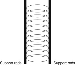
If the cathode is surrounded by a wire grid or mesh—in practice, this will usually take the form of a spiral coil, spot welded between two stiff supporting wires, of the form shown in Figure 11.2—the current flow from the cathode to the anode can be controlled by the voltage applied to the grid, such that if the grid is made positive, more negatively charged electrons will be attracted away from the cathode and encouraged to continue on their way to the anode. However, if the grid is made negative, it will repel the electrons emitted by the cathode and reduce the current flow to the anode.
Figure 11.2. Control grid construction.
It is this quality that is the most useful aspect of a valve in that a quite large anode current flow can be controlled by a relatively small voltage applied to the grid, and so long as the grid is not allowed to swing positive with respect to the cathode, no current will flow in the grid circuit, and its effective input impedance at low frequencies will be almost infinite. This ability to regulate a large current at a high voltage by a much smaller control voltage allows the valve to amplify small electrical signals, and since the relationship between grid voltage and anode current is relatively linear, as shown in Figure 11.3, this amplification will cause relatively little distortion in the amplified signal. The theoretical amplification factor of a valve, operating into an infinitely high impedance anode load, is denoted by the Greek symbol μ.
Figure 11.3. Triode valve characteristics.

Although there may be several grids between the cathode and the anode in more complex valves, the grid closest to the cathode will have the greatest influence on the anode current flow, which is therefore usually called the control grid.
The effectiveness of the grid in regulating the anode current depends on the relative proximity of the grid and the anode to the cathode, in that, if the grid is close to the cathode, but the anode is relatively remote, the effectiveness of the grid in determining the anode current will be much greater and will therefore give a higher value of μ than if the anode is closer to the grid and cathode. Unfortunately, there is a snag in that the anode current resistance of the valve, Ra, is also related to the anode/cathode spacing and becomes higher as the anode/cathode spacing is increased. The closeness of the pitch of the wire spiral that forms the grid also affects the anode current resistance in that a close spacing will lead to a high Ra, and vice versa.
The stage gain (M) of a simple valve amplifier, of the kind shown in Figure 11.4, is given by the equation
![]() so that a low impedance valve, such as a 6SN7 (typical Ia=9 mA, Ra=7.7 K, μ=20), which has close anode–grid and grid–cathode spacings, and a relatively open pitch in the grid wire spiral,
will have a high possible anode current but a low amplification factor, while a high impedance valve such as a 6SL7 (typical
Ia=2.3 mA, Ra=44 K, μ=70) will have a low stage gain unless the circuit used has a high value of anode load resistance (R), which, in turn, will demand a high value of HT voltage.
so that a low impedance valve, such as a 6SN7 (typical Ia=9 mA, Ra=7.7 K, μ=20), which has close anode–grid and grid–cathode spacings, and a relatively open pitch in the grid wire spiral,
will have a high possible anode current but a low amplification factor, while a high impedance valve such as a 6SL7 (typical
Ia=2.3 mA, Ra=44 K, μ=70) will have a low stage gain unless the circuit used has a high value of anode load resistance (R), which, in turn, will demand a high value of HT voltage.
Figure 11.4. A simple valve amplifier.

11.1.4. The Space Charge
Although a cloud of electrons will surround any heated cathode mounted in a vacuum and will act as a reservoir of electrons when these are drawn off as anode current, their presence becomes of particular importance when a negatively charged control grid is introduced into the system, in that the electron cloud will effectively fill the space between the cathode and the grid and will act as the principal source of electrons.
The presence of this electron cloud—known as the space charge—has several important operational advantages. Of these the first is that, by acting as an electron reservoir, it allows larger, brief-duration, current flows than would be available from the cathode on its own and that it acts as a measure of protection to the cathode against the impacts of positive ions created by electronic collisions with the residual gases in the envelope, as these ions will be attracted toward the more negatively charged cathode. Finally, left to itself, the electronic emission from the cathode suffers from both “shot” and “flicker” noise, a current fluctuation that is averaged out if the anode current is drawn from the space charge.
This random emission of electrons from a space charge-depleted cathode is used to advantage in a “noise diode,” a wide-band noise source that consists of a valve in which the cathode is deliberately operated at a low temperature to prevent a space charge from forming so that a resultant noisy current can be drawn off by the anode.
In the case of a triode used as an output power valve, where large anode currents are needed, the grid mesh must be coarse and the grid–cathode spacing must be close. This limits the formation of an adequate space charge in the grid–cathode gap, and, in its absence, the cathode must have higher emission efficiency than would be practicable with an indirectly heated system, which means that a directly heated filament must be used instead. Usually, the filament voltage will be low to minimize cathode-induced “hum” and the filament current will be high because of the size of the filament (2.5 A at 2.5 V in the case of the 2A3 valve).
Directly heated cathodes are also commonly used in valve HT rectifiers, such as the 5U4 or the 5Y3, because the higher cathode emission reduces the voltage drop across the valve and increases the available HT output voltage by comparison with a similar power supply using an indirectly heated cathode type.
11.1.5. Tetrodes and Pentodes
Although the triode valve has a number of advantages as an amplifier, such as a low noise and low distortion factor, it suffers from the snag that there will be a significant capacitance, typically of the order of 2.5 pF, between the grid and the anode. In itself, this latter capacitance would seem to be too small to be troublesome, but, in an amplifying stage with a gain of, say, 100, the Miller effect will increase the capacitance by a factor of 101, increasing the effective input capacitance to 252.5 pF, which could influence the performance of the stage.
When triode valves were used as RF amplifiers, in the early years of radio, this anode–grid capacitance caused unwanted RF instability, and the solution adopted was the introduction of a “screening” grid between the triode control grid and its anode, which reduced this anode–grid capacitance, in the case of a screened grid or tetrode valve, to some 0.025 pF.
A further effect that the inclusion of a screening grid had upon the valve characteristics was to make the anode current, in its linear region, almost independent of the anode voltage, which led to very high values for Ra and μ. Unfortunately, the presence of this grid caused a problem that when the anode voltage fell, during dynamic conditions, to less than that of the screening grid, electrons hitting the anode could cause secondary electrons to be ejected from its surface, especially if the anode was hot or its surface had been contaminated by cathode material, and these would be collected by the screening grid, which would cause a kink in the anode current/voltage characteristics. While this might not matter much in an RF amplifier, it would cause an unacceptable level of distortion if used in an audio amplifier stage.
Two solutions were found for this problem, of which the simplest was to interpose an additional, open mesh grid between the anode and the screening grid. This grid will normally be connected to the cathode, either externally or within the valve envelope, and is called the suppressor grid because it acts to suppress the emission of secondary electrons from the anode.
Since this type of valve had five electrodes it was called a “pentode.” A typical small-signal pentode designed specifically for use in audio systems is the EF86, in which steps have also been taken to reduce the problem of microphony when the valve is used in the early stages of an amplifying system. The EF86 also has a wire mesh screen inside the glass envelope and surrounding the whole of the electrode structure. This is connected to pins 2 and 7 and is intended to lessen the influence of external voltage fields on the electron flow between the valve electrodes.
In use, a small-signal pentode amplifying stage will give a much higher stage gain than a medium impedance triode valve (250˘ in comparison with, say, 30˘). It will also have a better HF gain due to its lower effective anode–grid capacitance. However, a triode gain stage will probably have a distortion figure, other things being equal, which is about half that of a pentode.
The second solution to the problem of anode current nonlinearity in tetrodes, particularly suited to the output stages of audio amplifiers, was alignment of the wires of the control grid and screening grid so that they constrained the electron flow into a series of beams, which served to sweep any secondary electrons back toward the anode—a process that was helped by the inclusion within the anode box of a pair of “beam-confining electrodes,” which modified the internal electrostatic field pattern. These are connected to the cathode internally and take the form shown in Figure 11.5. These valves were called beam tetrodes or kinkless tetrodes and had a lower distortion than output pentodes. Valves of this type, such as the 6L6, the 807, and the KT66 and KT88, were widely employed in the output stages of the high-quality audio amplifiers of the 1950s and early 1960s.
Figure 11.5. Construction of a beam tetrode.(Courtesy of RCA.)

Both pentodes and beam tetrodes can be used with their screen grids connected to their anodes. In this mode their characteristics will resemble a triode having similar grid–cathode and grid–anode spacings to the grid–cathode and grid–screen grid spacings of the pentode. The most common use of this form of connection is in power output stages, where a triode connected beam tetrode will behave much like a power triode, without the need for a directly heated (and hum-inducing) cathode.
11.1.6. Valve Parameters
In addition to the anode current resistance, Ra, and the amplification factor, μ, mentioned earlier, there is also the valve slope or mutual conductance (gm), which is a measure of the extent to which the anode current will be changed by a change in grid voltage. Traditionally, this would be quoted in milliamperes per volt (mA/V or milli-Siemens, written as mS) and would be a useful indication of the likely stage gain given by the valve in an amplifying circuit.
This would be particularly helpful in the case of a pentode amplifying stage, where the value of Ra would probably be very high in comparison with the likely value of load resistance. (For example, in the case of the EF86, Ra is quoted as 2.5 MΩ and the gm is 2 mA/V.) In this case, the stage gain (M) can be determined, approximately, by the relationship M≈–gm ∙ RL, which, for a 100 k anode load would be ≈2200˘.
The various valve characteristics are defined mathematically as

In these equations the negative sign takes account of the phase inversion of the signal. These parameters are related to one another by the further equation,
![]()
11.1.7. Gettering
Preservation of a high vacuum within its envelope is essential to the life expectancy and proper operation of the valve. However, it is difficult to remove all traces of residual gas on the initial pumping out of the envelope, quite apart from the small but continuing gas evolution from the cathode, or any other electrodes that may become hot in use. The solution to this problem is the inclusion of a small container, known as a boat, mounted somewhere within the envelope, but facing away from the valve electrodes, which contains a small quantity of reactive material, such as metallic calcium and magnesium.
The boat is positioned so that after the pumping out of the envelope has been completed, and the valve had been sealed off, the getter could be caused to evaporate on to the inner face of the envelope by heating the boat with an induction heating coil. Care is taken to ensure that as little as possible of the getter material finds its way on to the inner faces of the valve electrodes, where it may cause secondary emission, or on to the mica spacers, where it may cause leakage currents between the electrodes.
While this technique is reasonably effective in cleaning up the gas traces that arise during use of the valve, the vacuum is never absolute, and evidence of the residual gas can sometimes be seen as a faint, deep blue glow in the space within the anode envelope of a power output valve. If, however, there is a crack in the glass envelope, or some other cause of significant air leakage into the valve interior, this will become apparent because of a whitening of the edges of the normally dark, mirror-like surface of the getter deposit on the inside of the valve envelope. A further sign of the ingress of air into the valve envelope is the presence of a pinkish-violet glow that extends beyond the confines of the anode box. By this time the valve must be removed and discarded to prevent damage to other circuit components through an increasing and uncontrolled current flow.
11.1.8. Cathode and Heater Ratings
For optimum performance, the cathode temperature should be maintained, when in use, at its optimum value, which requires that the heater or filament voltages should be set at the correct levels. Since the voltage of the domestic AC power supply is not constant, the design ratings for the heater or filament supply must take account of this. However, this is not as difficult to do as it might appear. For example, Brimar, a well-known valve manufacturer, makes the following recommendations in their Valve and Teletube Manual: “the heater supply voltages should be within ±5% of the rated value when the heater transformer is fed with its nominal input voltage, provided that the mains power supply is within ±10% of its declared value.”
An additional requirement is that, because of inevitable cathode-heater leakage currents, the voltages between these electrodes should be kept as low as possible and should not exceed 200 V. Moreover, there must always be a resistive path, not exceeding 250 kΩ, between the cathode and heater circuits.
As a practical point, the wiring of the heater circuit, which is usually operated at 6.3 V AC, will normally be installed as a twisted pair to minimize the induction of mains hum into sensitive parts of the system, as will the heater wiring inside the cathode tube of low noise valves, such as the EF86. With modern components, such as silicon diodes and low-cost regulator ICs, there is no good reason why the heater supplies to high-quality valve amplifiers should not be derived from smoothed and stabilized DC sources.
It has been suggested that the cathodes of valves can be damaged by reverse direction ionic bombardment if the HT voltage is applied before the cathode has had a chance to warm up and form a space charge, and that the valve heaters should be left on to avoid this problem. In practice, this problem does not arise because gaseous ions are only formed by collisions between residual gas molecules and the electrons in the anode current stream. If the cathode has not reached operating temperature there will be little or no anode current and, consequently, no gaseous ions produced as a result of it. Brimar specifically warns against leaving the cathode heated, in the absence of anode current, in that this may lead to cathode poisoning because of chemical reactions occurring between the exposed reactive metal of the cathode surface and any gaseous contaminants present within the envelope. Unfortunately, the loss of electron emissivity as the cathode temperature is reduced occurs more rapidly than the reduction in the chemical reactivity of the cathode metals.
Indirectly heated HT rectifier valves have been used, despite their lower operating efficiency, to ensure that the full HT voltage was not applied to the equipment before the other valves had warmed up. This was done to avoid the HT rail overvoltage surge that would otherwise occur and allow the safe use of lower working voltage and less expensive components, such as HT reservoir, smoothing, or intervalve coupling capacitors.
11.1.9. Microphony
Any physical vibration of the grid (or filament, in the case of a directly heated cathode) will, by altering the grid–cathode spacing, cause a fluctuation of the anode current, which will cause an audible ringing sound when the envelope is tapped—an effect known as microphony in the case of a valve used in audio circuitry. Great care must therefore be taken in the manufacture of valves to maintain the firmness of the mounting of the grids and other electrodes. This is done by the use of rigid supporting struts whose ends are located in holes punched in stiff mica disc-shaped spacers, which, in turn, are a tight fit within the valve envelope.
Since a microphonic valve will pick up vibration from any sound source, such as a loudspeaker system in proximity to it, and convert these sounds into (inevitably distorted) electrical signals, which will be added to the amplifier output, this can be a significant, but unsuspected, source of signal distortion, which will not be revealed during laboratory testing on a resistive dummy load. Because it is difficult to avoid valve microphony completely, and it is equally difficult to sound proof amplifiers, this type of distortion will always occur unless such valve amplifier systems are operated at a low volume level or the amplifier is located in a room remote from the loudspeakers.
11.2. Solid-State Devices
11.2.1. Bipolar Junction Transistors
11.2.1.1. ‘N’- and ‘P’-Type Materials
Most materials can be grouped in one or other of three classes, insulators, semiconductors, or conductors, depending on the ease or difficulty with which electrons can pass through them. In insulators, all of the electrons associated with the atomic structure will be firmly bound in the valency bands of the material, whereas in good, usually metallic, conductors many of the atomic electrons will only be loosely bound and will be free to move within the body of the material.
In semiconductors, at temperatures above absolute zero (0°K or –273.15°C), electrons will exist both in the valency levels where they are not free to leave the atoms with which they are associated and in the conduction band in which they are free to travel within the body of the material. This characteristic is influenced greatly by the “doping” of the material, which is normally done during the manufacture of the semiconductor material by introducing carefully controlled amounts of specific impurities into the molten mass from which the single semiconductor crystal is grown. The most common semiconductor material in normal use is silicon because it is inexpensive, readily available, and has good thermal properties. Germanium, the material from which all early transistors were made, has electrical characteristics that are influenced greatly by its temperature, which is inconvenient in use. Also, it does not lend itself at all well to contemporary mass-production techniques.
In the case of silicon, which has very little conductivity in its undoped “intrinsic” form, the most common dopants are boron or aluminium, which give rise to a semiconductor with a deficiency of valency electrons, usually referred to as holes—called a ‘P’-type material—or phosphorus, which will cause the silicon to have a surplus of valency electrons, which forces some of them into the conduction band. Such a semiconductor material would be termed ‘N’ type. Both P-type and N-type silicon can be quite highly conductive, depending on the doping levels used.
11.2.1.2. Fermi Levels
The electron energy distribution in single-crystal P- and N-type materials is shown in Figure 11.6, and the mean electron energy levels, known as the Fermi levels, are shown.
Figure 11.6. An audio amplifier block diagram.

11.3. Valve Audio Amplifier Layouts
In its simplest form, shown in Figure 11.6, an audio amplifier consists of an input voltage amplifier stage (A) whose gain can be varied to provide the desired output signal level, an impedance converter stage (ZC) to adjust the output impedance of the amplifier to suit the load, which could be a loudspeaker, a pair of headphones, or the cutting head in a vinyl disc manufacturing machine.
In the case of headphones, their load impedance could be high enough for them to be driven directly by the voltage amplifier stage without a serious impedance mismatch, but with other types of output load it will be necessary to interpose some sort of impedance conversion device; in valve-operated audio systems this is most commonly an iron-cored audio frequency transformer. This is a difficult component to incorporate within a high-fidelity system, and much thought must be given both to its design and the way it is used in the circuit.
A very simple circuit layout embodying the structure outlined in Figure 11.6, using directly heated (battery operated) valves, is shown in Figure 11.7. This is the type of design that might have been built some 50 years ago by a technically minded youngster who wanted some means of driving a loudspeaker from a simple piezo-electric gramophone pick-up.
Figure 11.7. A simple valve amplifier.

For the maximum transfer of power from an amplifier to its load it is necessary that both of these should have the same impedance, and since the anode resistance (Ra) of the output valve is of the order of 10 kΩ, and the most common speech coil impedance of an inexpensive moving coil loudspeaker is 3 Ω, there would be a drastic loss of available power unless some impedance converting output transformer was employed.
The primary:secondary turns ratio of this component would need to be √(10 k/3)=58:1. It is difficult to design transformers having such high turns ratios without losses in performance; consequently, when higher audio quality was required, the LS manufacturers responded by making loudspeaker drive units with higher impedance speech coils. Before the advent of transistor-operated audio amplifiers the most common LS driver impedance was 15 Ω.
With regard to the amplifier design shown, the input stage (V1) uses a simple directly heated triode, with grid-current bias developed across the 4M7 Ω grid resistor, R1. This is resistor/capacitor coupled to V2, a small-power beam tetrode or pentode, operated with fixed bias derived from an external DC voltage source.
Because both V1 and V2 will contribute some distortion to the signal—in the case of V1, this will mainly be second harmonic, but in the output valve (V2) there will also be a substantial third harmonic component—the output signal will sound somewhat shrill due to the presence of these spurious high signal frequency components in the output. The simplest and most commonly adopted remedy for this defect was to connect a capacitor (C4) across the primary of the output transformer (TR1) to roll-off the high-frequency response of the amplifier as a whole to give it the required mellow sound. The HT line decoupling capacitor (C2) serves to reduce the amount of spurious and distorted audio signal, present on the +V supply line, which will be added to the wanted signal present on the V2 grid. An amplifier of this type would have an output power of, perhaps, 0.5 W, a bandwidth, mainly depending on the quality of the output transformer, that could be 150 Hz−6 kHz, ±6 dB, and a harmonic distortion, at 1 kHz and 0.4 W output, of 10%.
The amplifier shown in Figure 11.7 uses a circuit of the kind that would allow operation from batteries, and it was accepted that such designs would have a low output power and a relatively poor performance in respect to its audio quality: this was the price paid for the low current drain on its power source. If, however, the amplifier was to be powered from an AC mains supply, the constraints imposed by the need to keep the total current demand low no longer applied, which gave the circuit designer much greater freedom. The other consideration in the progress toward higher audio power outputs was the type of output stage layout, in that this influenced the output stage efficiency, as examined later.
11.4. Single-Ended Versus Push–Pull Operation
These two options are shown schematically in Figure 11.8, in which Q1 and Q2 are notional amplifier blocks, simplified to the extent that they are only considered as being either open-circuit (O/C) or short-circuit (S/C), but with some internal resistance, shown as R3 [or R1 in the case of Figure 11.8(b)]. I have also adopted the convention that the current flow into the load resistor (R2) is deemed to be positive when the amplifier circuit is feeding current (as a current source) into the load and to be negative when the amplifier is acting as a current sink and drawing current from R2 and its associated power supply. I have also labeled the voltage at the junction of these three resistors as Vx. The efficiency of the system can be considered as related to the extent of the change in the current through R2 brought about by the change from O/C to S/C in Q1 or Q2.
Figure 11.8. Output arrangements.


If we consider first the single-ended layout of Figure 11.8(a), when Q1 is O/C, the current flow into R2 is only through R1 and i2=V/(R1+R2). If, however, Q1 is short circuited, S/C, then, from inspection,(11.1)
![]() (11.2)
(11.2)
![]() (11.3)
(11.3)
![]() (11.4)
(11.4)
![]() from Equations (11.1), (11.2), and (11.3)we have(11.5)
from Equations (11.1), (11.2), and (11.3)we have(11.5)
![]() but it has been seen from Equation (11.4) that i3=Vx/R3(11.6)
but it has been seen from Equation (11.4) that i3=Vx/R3(11.6)
![]()
If we insert the actual values for R1, R2, and R3, we can discover the difference in output current flow in the load resistor (R2) between the O/C and S/C conditions of Q1. For example, if all resistors are 10 Ω in value, when Q1 is S/C, Vx will be equal to V, and there will be no current flow in R2 and the change on making Q1 O/C will be (V/20)A. If R1 and R2 are 10 Ω in value and R3 is 5 Ω, then the current flow in R2, when Q1 is O/C, will still be (V/20)A, whereas when Q1 is S/C, the current will be (–0.25 V/10)A and the change in current will be (3 V/40)A. By comparison, for the push–pull system of Figure 11.8(b), the change in current through R2, when this is 10 Ω and both R1 and R3 are 5 Ω in value, on the alteration in the conducting states of Q1 and Q2, will be (2 V/15)A, which is nearly twice as large.
The increase in available output power from similar output valves when operated at the same V+ line voltage in a push–pull rather than in a single-ended layout is the major advantage of this arrangement, although if the output devices have similar distortion characteristics, and the output transformer is well made, the even harmonic distortion components will tend to cancel. Also, the magnetization of the core of the output transformer due to the valve anode currents flowing in the two halves of the primary winding will be reduced substantially because the induced fields will be in opposition.
In addition, an increase in the drive voltage to the grids of the output valves, provided that it is not large enough to drive them into grid current, will, by reducing their equivalent series resistance (R1, R3 in the calculations given earlier), increase the available output power, whereas in the single-ended layout the dynamic drive current cannot be increased beyond twice the quiescent level without running into waveform clipping. However, there are other problems, which are discussed later.
11.5. Phase Splitters
In order to drive a pair of output valves in push–pull it is necessary to generate a pair of AC control grid drive voltages that are equal in magnitude but in phase opposition. The simplest way of doing this is to use a transformer as the anode load for an amplifier stage, but with a center-tapped secondary winding.
Figure 11.9 shows a typical center-tapped, transformer-coupled 20W audio amplifier, of the kind that would have been common in the period spanning the late 1930s to early 1940s. Because there are two coupling transformers in the signal path from the input and the LS output, which would cause substantial phase shifts at the ends of the audio spectrum, it would be impractical to try to clean up the amplifier’s relatively poor performance by applying overall negative feedback (from the LS output to V1 cathode) to the system.
Figure 11.9. A simple 20-W amplifier.

Some local negative feedback from anodes to grids in V2 and V3 is applied by way of C4/R4 and C6/R7 in an attempt to reduce the third, and other odd-order, harmonic distortion components generated by the output valves. Since the designer expected that the output sound quality could still be somewhat shrill, a pair of 0.05-μF capacitors, C7 and C8, has been added across the two halves of the output transformer primary windings to reduce the high-frequency performance. These would also have the effect of lessening the tendency of the output valves to flash over if the amplifier was driven into an open-circuited LS load—an endemic problem in designs without the benefit of overall negative feedback to stabilize the output voltage.
The anode voltage decoupling circuit (R3, C3), shown in Figure 11.9, is essential to prevent the spurious signal voltages from the +V supply line to the output valves being introduced to the output valve grid circuits. This would, in the absence of the supply line decoupling circuit, cause the amplifier to oscillate continuously at some low frequency—a problem that was called motorboating, from the sound produced in the loudspeakers.
Various circuit arrangements have been proposed as a means of generating a pair of low distortion, low phase shift, push–pull drive voltages. Of these, the phase inverter circuit of Figure 11.10 is the simplest, but does not offer a very high-quality performance. It is, in principle, a bad thing to attenuate and then to amplify again, as is done in this arrangement, because this simply adds just another increment of waveform distortion, due to V2, to that contributed by V1.
Figure 11.10. A simple phase inverter.

A much more satisfactory arrangement is that shown in Figure 11.11, in which V2 is operated as an anode follower, which, like the cathode follower, employs 100% negative feedback, although in this case derived from the anode. This stage contributes very little waveform distortion. Also, because both valves operate as normal amplifier stages, the available voltage from either output point will be largely unaffected by the operation of the circuit. An additional advantage over the circuit shown in Figure 11.10 is that the two antiphase output voltages are equal in magnitude, without the need to adjust the preset gain control, RV1.
Figure 11.11. A floating paraphase circuit.

Another satisfactory circuit is that based on the long-tailed pair layout, in which, provided that the tail resistor is large in relation to the cathode source resistance (1/gm), the two antiphase anode currents will be closely similar in magnitude. The advantage of this circuit is that it can be direct coupled (i.e., without the need for a DC blocking coupling capacitor) to the output of the preceding stage, which minimizes circuit phase shifts, especially at the LF end of the passband. By comparison with the two preceding phase-splitter circuits, it has the disadvantage that the available AC output swing, at either anode, is reduced greatly by the fact that the cathode voltages of V2 and V3 are considerably positive in relation to the 0-V line, which will almost certainly require an additional amplifier stage between its output and the input of any succeeding triode or beam-tetrode output stage.
This disadvantage is shared by the circuit layout shown in Figure 11.13, in which a direct-coupled triode amplifier is operated with identical value resistive loads in both its anode and cathode circuits. Because of the very high level of negative feedback due to the cathode resistor, both the distortion and the unwanted phase shifts introduced by this stage are very low. Significantly, this was the type of phase splitter adopted by D. T .N. Williamson in his classic 15-W audio amplifier design.
Figure 11.13. A split load phase splitter.

11.6. Output Stages
The basic choice of output valves will lie between a triode, a beam tetrode, or a pentode. If large output powers are required—say, in excess of 2 W—triode output valves are unsuitable because the physical spacing between the control grid and the anode must be small, and the grid mesh must be relatively widely spaced, in order to achieve a low anode current resistance and a high practicable anode current level. This closely packed type of construction will lead to the almost complete stripping of the space charge from the region between the cathode and the grid. Experience shows that the life expectancy of cathodes operated under such conditions is short, and the only way by which this problem can be avoided is by the use of a directly heated (filament type) cathode construction, which is much more prolific as a source of electrons, and this leads to other difficulties such as hum intrusion from the AC heater supplies, and the awkwardness of arranging cathode bias systems.
So, if it is required to use a triode output stage, at anything greater than the 50-mA anode current obtainable from a parallel connected 6N7 double triode (the 6SN7 has a smaller envelope and, in consequence, a lower permissible anode dissipation), a directly heated valve such as the now long obsolete 6B4 or PX25 would need to be found. Therefore, in practice, the choice for output valves will be between output beam tetrodes or pentodes. Although a fairly close simulation of a triode characteristic can be obtained in both of these valve types if the anode and G2 are connected together, this approach works better with a beam tetrode than a power output pentode because the presence of the suppressor grid in the pentode somewhat disturbs the anode current flow.
The required grid drive voltage for typical pentode or beam tetrode output valves, at Va=300 V, will be in the range of 20–50 Vp–p for each output valve, and whether or not the valve is triode connected has little effect on this requirement. The triode connection does, however, greatly affect the anode current impedance, which is reduced, in the case of the KT88, from 12 kΩ to 670 Ω, and the need for a lower turns ratio greatly simplifies the design of the necessary, load-matching, output transformer with low half-primary to half-primary and primary to secondary leakage inductances.
11.7. Output (Load-Matching) Transformer
This component is probably the most important factor in determining the quality of the sound given by a valve-operated audio amplifier, and the performance of this component is influenced by a number of factors, both mechanical and electrical, which will become of critical importance if an attempt is made to apply negative feedback (NFB) over the whole amplifier. However, for a low power system, such as might be used as a headphone amplifier, it is possible to make a quite decent sounding system without the need for much in the way of exotic components, circuit complexity, or very high-quality output impedance-matching transformers, and I have sketched out in Figure 11.14 a typical circuit for a two-valve, 1W headphone amplifier based on a pair of 6SN7s or equivalents.
Figure 11.14. A simple headphone amplifier.

In this design the input pair of valves acts as a floating paraphase phase-splitter circuit, which provides the drive for the output valves. Since the cathode currents from the two input valves are substantially identical, but opposite in phase, it is unnecessary to provide a cathode bypass capacitor to avoid loss of stage gain. Also, since this cathode resistor is common to both valves, it assists in reducing any differences between the two output signals, as the arrangement acts, in part, as a long-tailed pair circuit such as that shown in Figure 11.12. Since the total harmonic distortion from a push–pull pair of triodes will probably be less than 0.5% and will decrease as the output power is reduced, provided a reasonable quality output transformer is used, I have not included any overall NFB, which avoids any likely instability problems. To match the output impedances of V2A and V2B to a notional load impedance of 100 Ω, a transformer turns ratio, from total primary to secondary, of 12:1 is required.
Figure 11.12. A long-tailed pair circuit.

In more ambitious systems, in which NFB is used to improve the performance of the amplifier and reduce the distortion introduced by the output transformer, much more care is needed in the design of the circuit. In particular, the phase shifts in the signal that are introduced by the output transformer become very important if a voltage is to be derived from its output and fed back in antiphase to the input of the amplifier, in that to avoid instability the total phase angle within the feedback loop must not exceed 180° at any frequency at which the loop gain is greater than unity. This requirement can be met by both limiting the amount of NFB that is applied, which would, of course, limit its effectiveness, and controlling the gain/frequency characteristics of the system.
Although there are a number of factors that determine the phase shifts within the transformer, the two most important are the inductance of the primary winding and the leakage inductance between primary and secondary; a simple analysis of this problem, based on an idealized, loss-free transformer, can be made by reference to Figure 11.15. In this, R1 is the effective input resistance seen by the transformer, made up of the anode current resistance of the valve, in parallel with the effective load resistance, and L1 is the inductance of the transformer primary winding. When the signal frequency is lowered, a frequency will be reached at which there will be an attenuation of 3 dB and a phase shift of 60°. This will occur when R1=jωL1, where ω is the frequency in radians per seconds.
Figure 11.15. Equivalent circuits of idealized coupling transformer.

R2 is the secondary load resistance, which is the sum of the resistance reflected through the transformer and the anode resistance, and L2 is the primary leakage inductance—a term that denotes the lack of total inductive coupling between primary and secondary windings—which behaves like an inductance between the output and the load and introduces an attenuation, and associated phase shift, at the HF end of the passband. The HF –3-dB gain point, at which the phase shift will be 60°, will occur at a frequency at which R2=jωL2.
To see what these figures mean, consider the case of a 15-Ω resistive load, driven by a triode-connected KT66 that has an anode current resistance of 1000 ohms. Let us assume that, in order to achieve a low anode current distortion figure, it has been decided to provide an anode load of 5000 ohms. The turns ratio required will be √(5000/15)=18.25:1 and the effective input resistance (R1) due to the output load reflected through the transformer will be 833 ohms. If it is decided that the transformer shall have an LF −3-dB point at 10 Hz, then the primary inductance would need to be 833/2π10=833/62.8=13.26 H. If it is also decided that the HF –3-dB point is to be 50 kHz, then the leakage inductance must be 833/2π50,000=2.7 mH. The interesting feature here is that if an output pentode is used, which has a much higher value of Ra than a triode, not only will a higher primary inductance be required, but the leakage inductance can also be higher for the same HF phase error.
Unfortunately, a number of other factors affect the performance of the transformer. The first of these is the dependence of the permeability of the core material on the magnetizing flux density, as shown in Figure 11.16. Since the current through the windings in any audio application is continually changing, so therefore is the permeability, and with it the winding inductances and the phase errors introduced into the feedback loop. Williamson urged that, for good LF stability, the value of permeability, μ, for low values of B should be used for primary inductance calculations.
Figure 11.16. A magnetization curve.

Second, this change in inductance, as a function of current in the windings, is a source of transformer waveform distortion, as are—especially at high frequencies—the magnetic hysteresis of the core material and the eddy current losses in the core. These problems are exacerbated by the inevitable DC resistance of the windings and provide another reason, in addition to that of improved efficiency, for keeping the winding resistance as low as possible.
The third problem is that the permeability of the core material falls dramatically, as seen in Figure 11.16, if the magnetization force exceeds some effective core saturation level. This means that the cross-sectional area of the core (and the size and weight of the transformer) must be adequate if a distortion-generating collapse in the transformer output voltage is not to occur at high signal levels. The calculations here are essentially the same as those made to determine the minimum turns per volt figure permissible for the windings of a power transformer.[1]
In practical terms, the requirements of high primary inductance and low leakage inductance are conflicting and require that primary winding is divided into a number of sections between which portions of the secondary winding are interleaved. Williamson proposed that eight secondary segments should be placed in the gaps left between 10 primary windings. This increases the stray capacitance, C1, across the primary winding and between primary and secondary coils. However, the HF phase errors introduced by these will probably be unimportant within the design frequency spectrum.
11.8. Effect of Output Load Impedance
This is yet another area in which there is a conflict in design requirements, between output power and output stage distortion. Figure 11.17(a), shows the output power given for 1 and 2% THD values by a push–pull pair of U/L-connected KT88s in relation to the anode to anode load impedance chosen by the designer. These data are courtesy of the GEC[2] Since the distortion can also alter in its form as a function of load impedance, Figure 11.17(b) shows the way these circuit characteristics change as the load resistance changes. The figures given for a single-ended 6AK6 output pentode are due to Langford-Smith.[3]
Figure 11.17. (a) Power output vs THD. (b) Power output curve.


11.9. Available Output Power
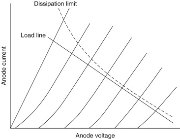
The power available from an audio amplifier, for a given THD figure, is an important aspect of the design. Although there are a number of factors that will influence this, such as the maximum permitted anode voltage or the maximum allowable cathode current, the first of these that must be considered is the permissible thermal dissipation of the anode of the valve. These limiting values are quoted in the manufacturers’ handbooks, and from these it is possible to draw a graph of the kind shown in Figure 11.18, where the maximum permitted combinations of anode current and anode voltage result in the curved (dashed) line indicating the dissipation limits for the valve, and the load line for its particular operating conditions can then be superimposed on this graph to confirm that the proposed working conditions will be within these thermal limits.
Figure 11.18. An anode dissipation curve.