8.5 MPSoCs and Shared Memory Multiprocessors
Shared memory processors are well-suited to applications that require a large amount of data to be processed. Signal processing systems stream data and can be well-suited to shared memory processing. Most MPSoCs are shared memory systems.
Shared memory allows for processors to communicate with varying patterns. If the pattern of communication is very fixed and if the processing of different steps is performed in different units, then a networked multiprocessor may be most appropriate. If the communication patterns between steps can vary, then shared memory provides that flexibility. If one processing element is used for several different steps, then shared memory also allows the required flexibility in communication.
8.5.1 Heterogeneous Shared Memory Multiprocessors
Many high-performance embedded platforms are heterogeneous multiprocessors. Different processing elements perform different functions. The PEs may be programmable processors with different instruction sets or specialized accelerators that provide little or no programmability. In both cases, the motivation for using different types of PEs is efficiency. Processors with different instruction sets can perform different tasks faster and using less energy. Accelerators provide even faster and lower-power operation for a narrow range of functions.
The next example studies the TI TMS320DM816x DaVinci digital media processor.
Example 8.3 TI TMS320DM816x DaVinci
The DaVinci 816x [Tex11, Tex11B] is designed for high-performance video applications. It includes both a CPU, a DSP, and several specialized units:

The 816x has two main programmable processors. The ARM Cortex A8 includes the Neon multimedia instructions. It is an in-order dual-issue machine. The C674x is a VLIW DSP. It has six ALUs and 64 general-purpose registers.
The HD video coprocessor subsystem (HDVICP2) provides image and video acceleration. It natively supports several standards, such as H.264 (used in BluRay), MPEG-4, MPEG-2, and JPEG. It includes specialized hardware for major image and video operations, including transform and quantization, motion estimation, and entropy coding. It also has its own DMA engine. It can operate at resolutions up to 1080P/I at 60 frames/sec. The HD video processing subsystem (HDVPSS) provides additional video processing capabilities. It can process up to three high-definition and one standard-definition video streams simultaneously. It can perform operations such as scan rate conversion, chromakey, and video security. The graphics unit is designed for 3D graphics operations that can process up to 30 M triangles/sec.
8.5.2 Accelerators
One important category of processing element for embedded multiprocessors is the accelerator. Accelerators can provide large performance increases for applications with computational kernels that spend a great deal of time in a small section of code. Accelerators can also provide critical speedups for low-latency I/O functions.
The design of accelerated systems is one example of hardware/software co-design—the simultaneous design of hardware and software to meet system objectives. Thus far, we have taken the computing platform as a given; by adding accelerators, we can customize the embedded platform to better meet our application’s demands.
As illustrated in Figure 8.23, a CPU accelerator is attached to the CPU bus. The CPU is often called the host. The CPU talks to the accelerator through data and control registers in the accelerator. These registers allow the CPU to monitor the accelerator’s operation and to give the accelerator commands.

Figure 8.23 CPU accelerators in a system.
The CPU and accelerator may also communicate via shared memory. If the accelerator needs to operate on a large volume of data, it is usually more efficient to leave the data in memory and have the accelerator read and write memory directly rather than to have the CPU shuttle data from memory to accelerator registers and back. The CPU and accelerator use synchronization mechanisms to ensure that they do not destroy each other’s data.
An accelerator is not a co-processor. A co-processor is connected to the internals of the CPU and processes instructions. An accelerator interacts with the CPU through the programming model interface; it does not execute instructions. Its interface is functionally equivalent to an I/O device, although it usually does not perform input or output.
The first task in designing an accelerator is determining that our system actually needs one. We have to make sure that the function we want to accelerate will run more quickly on our accelerator than it will executing as software on a CPU. If our system CPU is a small microcontroller, the race may be easily won, but competing against a high-performance CPU is a challenge. We also have to make sure that the accelerated function will speed up the system. If some other operation is in fact the bottleneck, or if moving data into and out of the accelerator is too slow, then adding the accelerator may not be a net gain.
Once we have analyzed the system, we need to design the accelerator itself. In order to have identified our need for an accelerator, we must have a good understanding of the algorithm to be accelerated, which is often in the form of a high-level language program. We must translate the algorithm description into a hardware design, a considerable task in itself. We must also design the interface between the accelerator core and the CPU bus. The interface includes more than bus handshaking logic. For example, we have to determine how the application software on the CPU will communicate with the accelerator and provide the required registers; we may have to implement shared memory synchronization operations; and we may have to add address generation logic to read and write large amounts of data from system memory.
Finally, we will have to design the CPU-side interface to the accelerator. The application software will have to talk to the accelerator, providing it data and telling it what to do. We have to somehow synchronize the operation of the accelerator with the rest of the application so that the accelerator knows when it has the required data and the CPU knows when it has received the desired results.
Field-programmable gate arrays (FPGAs) provide one useful platform for custom accelerators. An FPGA has a fabric with both programmable logic gates and programmable interconnect that can be configured to implement a specific function. Most FPGAs also provide on-board memory that can be configured with different ports for custom memory systems. Some FPGAs provide on-board CPUs to run software that can talk to the FPGA fabric. Small CPUs can also be implemented directly in the FPGA fabric; the instruction sets of these processors can be customized for the required function.
The next example describes an MPSoC with both an on-board multiprocessor and an FPGA fabric.
Example 8.4 Xilinx Zynq-7000
The Xilinx Zynq-7000 platform combines a processor system augmented with an FPGA fabric:

The main CPU is a two-processor ARM MPCore with two Cortex-A9 CPUs. The CPU platform includes a variety of typical I/O devices connected to the processor by an AMBA bus. The AMBA bus also provides a number of ports to the FPGA fabric which can be used to build custom logic, programmable processors, or embedded RAM.
8.5.3 Accelerator Performance Analysis
In this section, we are most interested in speedup: How much faster is the system with the accelerator than the system without it? We may, of course, be concerned with other metrics such as power consumption and manufacturing cost. However, if the accelerator doesn’t provide an attractive speedup, questions of cost and power will be moot.
Performance analysis of an accelerated system is a more complex task than what we have done thus far. In Chapter 6 we found that performance analysis of a CPU with multiple processes was more complex than the analysis of a single program. When we have multiple processing elements, the task becomes even more difficult.
The speedup factor depends in part on whether the system is single threaded or multithreaded, that is, whether the CPU sits idle while the accelerator runs in the single-threaded case or the CPU can do useful work in parallel with the accelerator in the multithreaded case. Another equivalent description is blocking versus nonblocking: Does the CPU’s scheduler block other operations and wait for the accelerator call to complete, or does the CPU allow some other process to run in parallel with the accelerator? The possibilities are shown in Figure 8.24. Data dependencies allow P2 and P3 to run independently on the CPU, but P2 relies on the results of the A1 process that is implemented by the accelerator. However, in the single-threaded case, the CPU blocks to wait for the accelerator to return the results of its computation. As a result, it doesn’t matter whether P2 or P3 runs next on the CPU. In the multithreaded case, the CPU continues to do useful work while the accelerator runs, so the CPU can start P3 just after starting the accelerator and finish the task earlier.

Figure 8.24 Single-threaded vs. multithreaded control of an accelerator.
The first task is to analyze the performance of the accelerator. As illustrated in Figure 8.25, the execution time for the accelerator depends on more than just the time required to execute the accelerator’s function. It also depends on the time required to get the data into the accelerator and back out of it.
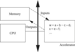
Figure 8.25 Components of execution time for an accelerator.
Because the CPU’s registers are probably not addressable by the accelerator, the data probably reside in main memory.
Accelerator execution time
A simple accelerator will read all its input data, perform the required computation, and then write all its results. In this case, the total execution time may be written as
![]() (Eq. 8.1)
(Eq. 8.1)
where tx is the execution time of the accelerator assuming all data are available, and tin and tout are the times required for reading and writing the required variables, respectively. The values for tin and tout must reflect the time required for the bus transactions, including two factors:
• the time required to flush any register or cache values to main memory, if those values are needed in main memory to communicate with the accelerator; and
• the time required for transfer of control between the CPU and accelerator.
Transferring data into and out of the accelerator may require the accelerator to become a bus master. Because the CPU may delay bus mastership requests, some worst-case value for bus mastership acquisition must be determined based on the CPU characteristics.
A more sophisticated accelerator could try to overlap input and output with computation. For example, it could read a few variables and start computing on those values while reading other values in parallel. In this case, the tin and tout terms would represent the nonoverlapped read/write times rather than the complete input and output times. One important example of overlapped I/O and computation is streaming data applications such as digital filtering. As illustrated in Figure 8.26 an accelerator may take in one or more streams of data and output a stream. Latency requirements generally require that outputs be produced on the fly rather than storing up all the data and then computing; furthermore, it may be impractical to store long streams at all. In this case, the tin and tout terms are determined by the amount of data read in before starting computation and the length of time between the last computation and the last data output.
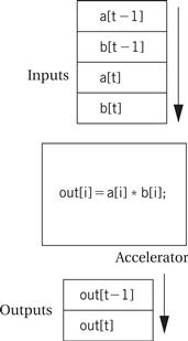
Figure 8.26 Streaming data into and out of an accelerator.
We are most interested in the speedup obtained by replacing the software implementation with the accelerator. The total speedup S for a kernel can be written as [Hen94]:
![]() (Eq. 8.2)
(Eq. 8.2)
where tCPU is the execution time of the equivalent function in software on the CPU and n is the number of times the function will be executed. We can use the techniques of Chapter 5 to determine the value of tCPU . Clearly, the more times the function is evaluated, the more valuable the speedup provided by the accelerator becomes.
System speedup
Ultimately, we care not so much about the accelerator’s speedup as the speedup for the complete system—that is, how much faster the entire application completes execution. In a single-threaded system, the evaluation of the accelerator’s speedup to the total system speedup is simple: The system execution time is reduced by S. The reason is illustrated in Figure 8.27—the single thread of control gives us a single path whose length we can measure to determine the new execution speed.

Figure 8.27 Evaluating system speedup in a single-threaded implementation.
Evaluating system speedup in a multithreaded environment requires more subtlety. As shown in Figure 8.28, there is now more than one execution path. The total system execution time depends on the longest path from the beginning of execution to the end of execution. In this case, the system execution time depends on the relative speeds of P3 and P2 plus A1. If P2 and A1 together take the most time, P3 will not play a role in determining system execution time. If P3 takes longer, then P2 and A1 will not be a factor. To determine system execution time, we must label each node in the graph with its execution time. In simple cases we can enumerate the paths, measure the length of each, and select the longest one as the system execution time. Efficient graph algorithms can also be used to compute the longest path.

Figure 8.28 Evaluating system speedup in a multithreaded implementation.
This analysis shows the importance of selecting the proper functions to be moved to the accelerator. Clearly, if the function selected for speedup isn’t a big portion of system execution time, taking the number of times it is executed into account, you won’t see much system speedup. We also learned from Equation 8.2 that if too much overhead is incurred getting data into and out of the accelerator, we won’t see much speedup.
8.5.4 Scheduling and Allocation
When designing a distributed embedded system, we must deal with the scheduling and allocation design problems described below.
• We must schedule operations in time, including communication on the network and computations on the processing elements. Clearly, the scheduling of operations on the PEs and the communications between the PEs are linked. If one PE finishes its computations too late, it may interfere with another communication on the network as it tries to send its result to the PE that needs it. This is bad for both the PE that needs the result and the other PEs whose communication is interfered with.
• We must allocate computations to the processing elements. The allocation of computations to the PEs determines what communications are required—if a value computed on one PE is needed on another PE, it must be transmitted over the network.
Example 8.5 illustrates scheduling and allocation in accelerated embedded systems.
Example 8.5 Scheduling and Allocating Processes on a Distributed Embedded System
We can specify the system as a task graph. However, different processes may end up on different processing elements. Here is a task graph:

We have labeled the data transmissions on each arc so that we can refer to them later. We want to execute the task on the platform below.

The platform has two processing elements and a single bus connecting both PEs. To make decisions about where to allocate and when to schedule processes, we need to know how fast each process runs on each PE. Here are the process speeds:
The dash () entry signifies that the process cannot run on that type of processing element. In practice, a process may be excluded from some PEs for several reasons. If we use an ASIC to implement a special function, it will be able to implement only one process. A small CPU such as a microcontroller may not have enough memory for the process’s code or data; it may also simply run too slowly to be useful. A process may run at different speeds on different CPUs for many reasons; even when the CPUs run at the same clock rate, differences in the instruction sets can cause a process to be better suited to a particular CPU.
| M1 | M2 | |
| P1 | 5 | 5 |
| P2 | 5 | 6 |
| P3 | – | 5 |
If two processes are allocated to the same PE, they can communicate using the PE’s internal memory and incur no network communication time. Each edge in the task graph corresponds to a data communication that must be carried over the network. Because all PEs communicate at the same rate, the data communication rate is the same for all transmissions between PEs. We need to know how long each communication takes. In this case, d1 is a short message requiring 2 time units and d2 is a longer communication requiring 4 time units.
As an initial design, let us allocate P1 and P2 to M1 and P3 to M2. This allocation would, on the surface, appear to be a good one because P1 and P2 are both placed on the processor that runs them the fastest. This schedule shows what happens on all the processing elements and the network:

The schedule has length 19. The d1 message is sent between the processes internal to P1 and does not appear on the bus.
Let’s try a different allocation: P1 on M1 and P2 and P3 on M2. This makes P2 run more slowly. Here is the new schedule:

The length of this schedule is 18, or one time unit less than the other schedule. The increased computation time of P2 is more than made up for by being able to transmit a shorter message on the bus. If we had not taken communication into account when analyzing total execution time, we could have made the wrong choice of which processes to put on the same processing element.