
Chapter 15. Representation of Audio Signals
The impact that digital methods have made on audio has been at least as remarkable as it was on computing. Ian Sinclair uses this chapter to introduce the digital methods that seem so alien to anyone trained in analogue systems.
15.1. Introduction
The term digital audio is used so freely by so many that you could be excused for thinking there was nothing much new to tell. It is easy in fast conversation to present the impression of immense knowledge on the subject but it is more difficult to express the ideas concisely yet readably. The range of topics and disciplines that need to be harnessed in order to cover the field of digital audio is very wide and some of the concepts may appear paradoxical at first sight. One way of covering the topics would be to go for the apparent precision of the mathematical statement but, although this has its just place, a simpler physical understanding of the principles is of greater importance here. Thus in writing this chapter we steer between excessive arithmetic precision and ambiguous oversimplified description.
15.2. Analogue and Digital
Many of the physical things that we can sense in our environment appear to us to be part of a continuous range of sensation. For example, throughout the day much of coastal England is subject to tides. The cycle of tidal height can be plotted throughout the day. Imagine a pen plotter marking the height on a drum in much the same way as a barograph is arranged (Figure 15.1). The continuous line that is plotted is a feature of analogue signals in which the information is carried as a continuous infinitely fine variation of a voltage, current, or, as in this case, height of the sea level.
Figure 15.1. The plot of tidal height versus diurnal time for Portsmouth, United Kingdom, time in hours. Mariners will note the characteristically distorted shape of the tidal curve for the Solent. We could mark the height as a continuous function of time using the crude arrangement shown.

When we attempt to take a measurement from this plot we will need to recognize the effects of limited measurement accuracy and resolution. As we attempt greater resolution we will find that we approach a limit described by the noise or random errors in the measurement technique. You should appreciate the difference between resolution and accuracy since inaccuracy gives rise to distortion in the measurement due to some nonlinearity in the measurement process. This facility of measurement is useful. Suppose, for example, that we wished to send the information regarding the tidal heights we had measured to a colleague in another part of the country. One, admittedly crude, method might involve turning the drum as we traced out the plotted shape while at the far end an electrically driven pen wrote the same shape onto a second drum [Figure 15.2(a)]. In this method we would be subject to the nonlinearity of both the reading pen and the writing pen at the far end. We would also have to come to terms with the noise that the line, and any amplifiers, between us would add to the signal describing the plot. This additive property of noise and distortion is characteristic of handling a signal in its analogue form and, if an analogue signal has to travel through many such links, then it can be appreciated that the quality of the analogue signal is abraded irretrievably.
Figure 15.2. Sending tidal height data to a colleague in two ways: (a) by tracing out the curve shape using a pen attached to a variable resistor and using a meter driven pen at the far end and (b) by calling out numbers, having agreed what the scale and resolution of the numbers will be.


As a contrast consider describing the shape of the curve to your colleague by measuring the height of the curve at frequent intervals around the drum [Figure 15.2(b)]. You’ll need to agree first that you will make the measurement at each 10-min mark on the drum, for example, and you will need to agree on the units of the measurement. Your colleague will now receive a string of numbers from you. The noise of the line and its associated amplifiers will not affect the accuracy of the received information since the received information should be a recognizable number. The distortion and noise performance of the line must be gross for the spoken numbers to be garbled and thus you are very well assured of correctly conveying the information requested. At the receiving end the numbers are plotted on to the chart and, in the simplest approach, they can be simply joined up with straight lines. The result will be a curve looking very much like the original.
Let’s look at this analogy a little more closely. We have already recognized that we have had to agree on the time interval between each measurement and on the meaning of the units we will use. The optimum choice for this rate is determined by the fastest rate at which the tidal height changes. If, within the 10-minute interval chosen, the tidal height could have ebbed and flowed then we would find that this nuance in the change of tidal height would not be reflected in our set of readings. At this stage we would need to recognize the need to decrease the interval between readings. We will have to agree on the resolution of the measurement, since, if an arbitrarily fine resolution is requested, it will take a much longer time for all of the information to be conveyed or transmitted. We will also need to recognize the effect of inaccuracies in marking off the time intervals at both the transmit or coding end and the receiving end since this is a source of error that affects each end independently.
In this simple example of digitizing a simple wave shape we have turned over a few ideas. We note that the method is robust and relatively immune to noise and distortion in the transmission and we note also that, provided we agree on what the time interval between readings should represent, small amounts of error in the timing of the reception of each piece of data will be completely removed when the data are plotted. We also note that greater resolution requires a longer time and that the choice of time interval affects our ability to resolve the shape of the curve. All of these concepts have their own special terms and we will meet them slightly more formally.
In the example just given we used implicitly the usual decimal base for counting. In the decimal base there are 10 digits (0 through 9). As we count beyond 9 we adopt the convention that we increment our count of the number of tens by one and recommence counting in the units column from 0. The process is repeated for the count of hundreds, thousands, and so on. Each column thus represents the number of powers of 10 (10=101, 100=102, 1000=103, and so on). We are not restricted to using the number base of 10 for counting. Among the bases in common use these days are base 16 (known more commonly as the hexadecimal base), base 8 (known as octal), and the simplest of them all, base 2 (known as binary). Some of these scales have been, and continue to be, in common use. We recognize that the old coinage system in the United Kingdom used the base of 12 for pennies, as, indeed, the old way of marking distance still uses the unit of 12 inches to a foot.
The binary counting scale has many useful properties. Counting in the base of 2 means that there can only be two unique digits, 1 and 0. Thus each column must represent a power of 2 (2=21, 4=22, 8=23, 16=24, and so on) and, by convention, we use a 1 to mark the presence of a power of 2 in a given column. We can represent any number by adding up an appropriate collection of powers of 2 and, if you try it, remember that 20 is equal to 1. We refer to each symbol as a bit (actually a contraction of the words binary digit). The bit that appears in the units column is referred to as the least significant bit ( LSB), and the bit position that carries the most weight is referred to as the most significant bit (MSB).
Binary arithmetic is relatively easy to perform since the result of any arithmetic operation on a single bit can only be either 1 or 0.
We have two small puzzles at this stage. The first concerns how we represent numbers that are smaller than unity and the second is how negative numbers are represented. In the everyday decimal (base of 10) system we have adopted the convention that numbers which appear to the right of the decimal point indicate successively smaller values. This is in exactly the opposite way in which numbers appearing to the left of the decimal point indicated the presence of increasing powers of 10. Thus successive columns represent 0.1=1/10=10−1, 0.01=1/100=10−2, 0.001=1/1000=10−3, and so on. We follow the same idea for binary numbers and thus the successive columns represent 0.5=1/2=2−1, 0.25=1/4=2−2, 0.125=1/8=2−3, and so on.
One of the most useful properties of binary numbers is the ease with which arithmetic operations can be carried out by simple binary logic. For this to be viable there has to be a way of including some sign in the number itself since we have only the two symbols 0 and 1. Here are two ways it can be done. We can add a 1 at the beginning of the number to indicate that it was negative or we can use a more flexible technique known as two’s complement. Here the positive numbers appear as we would expect but the negative numbering is formed by subtracting the value of the intended negative number from the largest possible positive number incremented by 1. Table 15.1 shows both of these approaches. The use of a sign bit is only possible because we will arrange that we will use the same numbering and marking convention. We will thus know the size of the largest positive or negative number we can count to. The simple use of a sign bit leads to two values for zero, which is not elegant or useful. One of the advantages of two’s complement coding is that it makes subtraction simply a matter of addition. Arithmetic processes are at the heart of digital signal processing and thus hold the key to handling digitized audio signals.
Table 15.1. Four-Bit Binary Number Coding Methods
| Binary number representation | |||
|---|---|---|---|
| Decimal number | Sign plus magnitude | Two’s complement | Offset binary |
| 7 | 0011 | 0111 | 1111 |
| 6 | 0110 | 0110 | 1110 |
| 5 | 0101 | 0101 | 1101 |
| 4 | 0100 | 0100 | 1100 |
| 3 | 0011 | 0011 | 1011 |
| 2 | 0010 | 0010 | 1010 |
| 1 | 0001 | 0001 | 1001 |
| 0 | 0000 | 0000 | 1000 |
| −0 | 1000 | (0000) | (1000) |
| −1 | 1001 | 1111 | 0111 |
| −2 | 1010 | 1110 | 0110 |
| −3 | 1011 | 1101 | 0101 |
| −4 | 1100 | 1100 | 0100 |
| −5 | 1101 | 1011 | 0011 |
| −6 | 1110 | 1010 | 0010 |
| −7 | 1111 | 1001 | 0001 |
| −8 | 1000 | 0000 | |
There are many advantages to be gained by handling analogue signals in digitized form and, in no particular order, they include:
- great immunity from noise since the digitized signal can only be 1 or 0;
- exactly repeatable behavior;
- ability to correct for errors when they do occur;
- simple arithmetic operations, very easy for computers;
- more flexible processing possible and easy programmability;
- low cost potential; and
- processing can be independent of real time.
15.3. Elementary Logical Processes
We have described an outline of a binary counting scale and shown how we may implement a count using it but some physical method of performing this is needed. We can represent two states, a 1 and an 0 state, by using switches since their contacts will be either open or closed and there is no half-way state. Relay contacts also share this property but there are many advantages in representing the 1 and 0 states by the polarity or existence of a voltage or a current, not least of which is the facility of handling such signals at very high speed in integrated circuitry. Manipulation of the 1 and 0 signals is referred to as logic and, in practice, is usually implemented by simple logic circuits called gates. Digital integrated circuits comprise collections of various gates, which can number from a single gate (as in the eight input NAND gate exemplified by the 74LS30 part number) to many millions (as can be found in some microprocessors).
All logic operations can be implemented by the appropriate combination of just three operations:
- the AND gate, circuit symbol &, arithmetic symbol ‘.’;
- the OR gate, circuit symbol |, arithmetic symbol ‘+’; and
- the inverter or NOT gate, circuit and arithmetic symbol ‘−’.
From this primitive trio we can derive the NAND, NOR, and EXOR (exclusive-OR gate). Gates are characterized by the relationship of their output to combinations of their inputs (Figure 15.3). Note how the NAND (literally negated AND gate) performs the same logical function as OR gate fed with inverted signals and, similarly, note the equivalent duality in the NOR function. This particular set of dualities is known as De Morgan’s theorem.
Figure 15.3. Symbols and truth tables for the common basic gates. For larger arrays of gates it is more useful to express the overall logical function as a set of sums (the OR function) and products (the AND function); this is the terminology used by gate array designers.
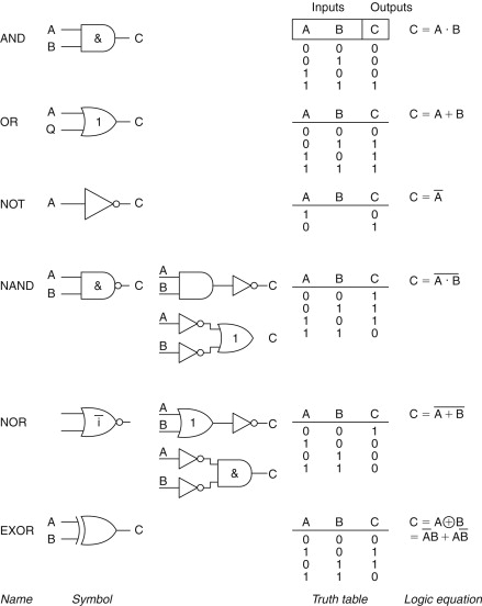
Practical logic systems are formed by grouping many gates together and naturally there are formal tools available to help with the design, the most simple and common of which is known as Boolean algebra. This is an algebra that allows logic problems to be expressed in symbolic terms. These can then be manipulated and the resulting expression can be directly interpreted as a logic circuit diagram. Boolean expressions cope best with logic that has no timing or memory associated with it: for such systems other techniques, such as state machine analysis, are better used instead.
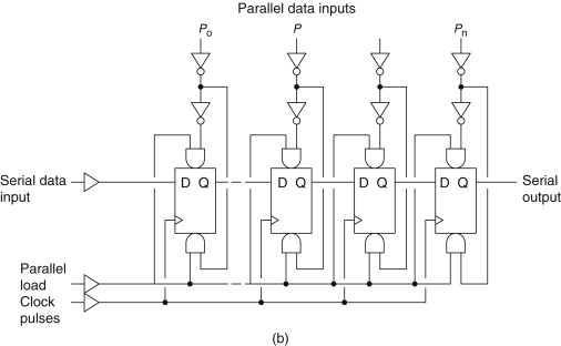
The simplest arrangement of gates that exhibit memory, at least while power is still applied, is the cross-coupled NAND (or NOR) gate (Figure 15.4). More complex arrangements produce the wide range of flip-flop (FF) gates, including the set–reset latch, the D-type FF, which is edge triggered by a clock pulse, the JK FF and a wide range of counters (or dividers), and shift registers (Figure 15.5). These circuit elements and their derivatives find their way into the circuitry of digital signal handling for a wide variety of reasons. Early digital circuitry was based around standardized logic chips, but it is much more common nowadays to use application-specific ICs.
Figure 15.4. A simple latch. In this example, the outputs of each of two NAND gates are cross coupled to one of the other inputs. The unused input is held high by a resistor to the positive supply rail. The state of the gate outputs will be changed when one of the inputs is grounded and this output state will be steady until the other input is grounded or until the power is removed. This simple circuit, the R-S flip-flop, has often been used to debounce mechanical contacts and as a simple memory.

Figure 15.5(a). The simplest counter is made up of a chain of edge-triggered D-type FFs. For a long counter, it can take a sizeable part of a clock cycle for all of the counter FFs to change state in turn. This ripple through can make decoding the state of the counter difficult and can lead to transitory glitches in the decoder output, indicated in the diagram as points where the changing edges do not exactly line up. Synchronous counters in which the clock pulse is applied to all of the counting FFs at the same time are used to reduce the overall propagation delay to that of a single stage.

Figure 15.5(b). This arrangement of FFs produces the shift register. In this circuit, a pattern of Is and 0 s can be loaded into a register (the load pulses) and then can be shifted out serially one bit at a time at a rate determined by the serial clock pulse. This is an example of a parallel in serial out (PISO) register. Other varieties include LIFO (last in first out), SIPO (serial in parallel out), and FILO (first in last out). The diagrams assume that unused inputs are tied to ground or to the positive supply rail as needed.
15.4. The Significance of Bits and Bobs
Groupings of eight bits, which represent a symbol or a number, are usually referred to as bytes, and the grouping of four bits is, somewhat obviously, sometimes called a nibble (sometimes spelt nybble). Bytes can be assembled into larger structures, which are referred to as words. Thus a three byte word will comprise 24 bits (though word is by now being used mainly to mean two bytes and DWord to mean four bytes). Blocks are the next layer of structure perhaps comprising 512 bytes (a common size for computer hard discs). Where the arrangement of a number of bytes fits a regular structure the term frame is used. We will meet other terms that describe elements of structure in due course.
Conventionally we think of bits, and their associated patterns and structures, as being represented by one of two voltage levels. This is not mandatory and there are other ways of representing the on/off nature of the binary signal. You should not forget alternatives such as the use of mechanical or solid state switches, presence or absence of a light, polarity of a magnetic field, state of waveform phase, and direction of an electric current. The most common voltage levels referred to are those used in the common 74×00 logic families and are often referred to as TTL levels. A logic 0 (or low) will be any voltage that is between 0 and 0.8 V while a logic 1 (or high) will be any voltage between 2.0 V and the supply rail voltage, which will be typically 5.0 V. In the gap between 0.8 and 2.0 V the performance of a logic element or circuit is not reliably determinable as it is in this region where the threshold between low and high logic levels is located. Assuming that the logic elements are being used correctly, the worst-case output levels of the TTL families for a logic 0 is between 0 and 0.5 V and for a logic 1 is between 2.4 V and the supply voltage. The difference between the range of acceptable input voltages for a particular logic level and the range of outputs for the same level gives the noise margin. Thus for TTL families, the noise margin is typically in the region of 0.4 V for both logic low and logic high. Signals whose logic levels lie outside these margins may cause misbehavior or errors and it is part of the skill of the design and layout of such circuitry that this risk is minimized.
Logic elements made using CMOS technologies have better input noise margins because the threshold of a CMOS gate is approximately equal to half of the supply voltage. Thus, after considering the inevitable spread of production variation and the effects of temperature, the available input range for a logic low (or 0) lies in the range 0 to 1.5 V and for a logic high (or 1) in the range of 3.5 to 5.0 V (assuming a 5.0-V supply). However, the output impedance of CMOS gates is at least three times higher than that for simple TTL gates and thus in a 5.0-V supply system interconnections in CMOS systems are more susceptible to reactively coupled noise. CMOS systems produce their full benefit of high noise margin when they are operated at higher voltages but this is not possible for CMOS technologies intended to be compatible with 74×00 logic families.
15.5. Transmitting Digital Signals
There are two ways in which you can transport bytes of information from one circuit or piece of equipment to another. Parallel transmission requires a signal line for each bit position and at least one further signal that will indicate that the byte now present on the signal lines is valid and should be accepted. Serial transmission requires that the byte be transmitted one bit at a time and in order that the receiving logic or equipment can recognize the correct beginning of each byte of information it is necessary to incorporate some form of signaling in serial data in order to indicate (as a minimum) the start of each byte. Figure 15.6 shows an example of each type.
Figure 15.6(a). Parallel transmission: a data strobe line
![]() (the—sign means active low) would accompany the bit pattern to clock the logic state of each data line on its falling edge
and is timed to occur some time after the data signals have been set so that any reflections, cross talk, or skew in the timing
of the individual data lines will have had time to settle. After the
(the—sign means active low) would accompany the bit pattern to clock the logic state of each data line on its falling edge
and is timed to occur some time after the data signals have been set so that any reflections, cross talk, or skew in the timing
of the individual data lines will have had time to settle. After the
![]() signal has returned to the high state, the data lines are reset to 0 (usually they would only be changed if data in the next
byte required a change).
signal has returned to the high state, the data lines are reset to 0 (usually they would only be changed if data in the next
byte required a change).

Figure 15.6(b). Serial transmission requires the sender and receiver to use and recognize the same signal format or protocol, such as RS232. For each byte, the composite signal contains a start bit, a parity bit, and a stop bit using inverted logic (1=−12 V; 0=−12 V). The time interval between each bit of the signal (the start bit, parity bit, stop bit, and data bits) is fixed and must be kept constant.

Parallel transmission has the advantage that, where it is possible to use a number of parallel wires, the rate at which data can be sent can be very high. However, it is not easy to maintain a very high data rate on long cables using this approach and its use for digital audio is usually restricted to the internals of equipment and for external use as an interface to peripheral devices attached to a computer.
The serial link carries its own timing with it and thus it is free from errors due to skew and it clearly has benefits when the transmission medium is not copper wire but infra-red or radio. It also uses a much simpler single circuit cable and a much simpler connector. However, the data rate will be roughly 10 times that for a single line of a parallel interface. Achieving this higher data rate requires that the sending and receiving impedances are accurately matched to the impedance of the connecting cable. Failure to do this will result in signal reflections, which in turn will result in received data being in error. This point is of practical importance because the primary means of conveying digital audio signals between equipments is by the serial AES/EBU signal interface at a data rate approximately equal to 3 Mbits per second.
You should refer to a text on the use of transmission lines for a full discussion of this point but for guidance here is a simple way of determining whether you will benefit by considering the transmission path as a transmission line.
- Look up the logic signal rise time, tR.
- Determine the propagation velocity in the chosen cable, v. This will be typically about 0.6 of the speed of light.
- Determine the length of the signal path, l.
- Calculate the propagation delay, τ=l/v.
- Calculate the ratio of tR/τ.
- If the ratio is greater than 8, then the signal path can be considered electrically short and you will need to consider the signal path’s inductance or capacitance, whichever is dominant.
- If the ratio is less than 8, then consider the signal path in terms of a transmission line.
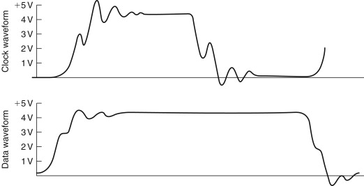
The speed at which logic transitions take place determines the maximum rate at which information can be handled by a logic system. The rise and fall times of a logic signal are important because of the effect on integrity. The outline of the problem is shown in Figure 15.7, which has been taken from a practical problem in which serial data were being distributed around a large digitally controlled audio mixing desk. Examples such as this illustrate the paradox that digital signals must, in fact, be considered from an analogue point of view.
Figure 15.7. A practical problem arose where the data signal was intended to be clocked in using the rising edge of a separate clock line, but excessive ringing on the clock line caused the data line to be sampled twice, causing corruption. In addition, due to the loading of a large number of audio channels, the actual logic level no longer achieved the 4.5-V target required for acceptable noise performance, increasing the susceptibility to ringing. The other point to note is that the falling edge of the logic signals took the data line voltage to a negative value, and there is no guarantee that the receiving logic element would not produce an incorrect output as a consequence.
15.6. The Analogue Audio Waveform
It seems appropriate to ensure that there is agreement concerning the meaning attached to words that are freely used. Part of the reason for this is in order that a clear understanding can be obtained into the meaning of phase. The analogue audio signal that we will encounter when it is viewed on an oscilloscope is a causal signal. It is considered as having zero value for negative time and it is also continuous with time. If we observe a few milliseconds of a musical signal we are very likely to observe a waveform that can be seen to have an underlying structure (Figure 15.8). Striking a single string can produce a waveform that appears to have a relatively simple structure. The waveform resulting from striking a chord is visually more complex, although, at any one time, a snapshot of it will show the evidence of structure. From a mathematical or analytical viewpoint the complicated waveform of real sounds is impossibly complex to handle and, instead, the analytical, and indeed the descriptive, process depends on us understanding the principles through the analysis of much simpler waveforms. We rely on the straightforward principle of superposition of waveforms such as the simple cosine wave.
Figure 15.8. (a) An apparently simple noise, such as a single string on a guitar, produces a complicated waveform, sensed in terms of pitch. The important part of this waveform is the basic period of the waveform, its fundamental frequency. The smaller detail is due to components of higher frequency and lower level. (b) An alternative description is analysis into the major frequency components. If processing accuracy is adequate, then the description in terms of amplitudes of harmonics (frequency domain) is identical to the description in terms of amplitude and time (time domain).


On its own an isolated cosine wave, or real signal, has no phase. However, from a mathematical point of view the apparently simple cosine wave signal, which we consider as a stimulus to an electronic system, can be considered more properly as a complex wave or function that is accompanied by a similarly shaped sine wave (Figure 15.9). It is worthwhile throwing out an equation at this point to illustrate this:
![]() where f(t) is a function of time, t, which is composed of Re f(t), the real part of the function and j Im f(t), the imaginary part of the function and j is √−1.
where f(t) is a function of time, t, which is composed of Re f(t), the real part of the function and j Im f(t), the imaginary part of the function and j is √−1.
Figure 15.9. The relationship between cosine (real) and sine (imaginary) waveforms in the complex exponential eJWT. This assists in understanding the concept of phase. Note that one property of the spiral form is that its projection onto any plane parallel to the time axis will produce a sinusoidal waveform.

Emergence of the √−1 is the useful part here because you may recall that analysis of the simple analogue circuit (Figure 15.10) involving resistors and capacitors produces an expression for the attenuation and the phase relationship between input and output of that circuit, which is achieved with the help of √−1.
Figure 15.10. The simple resistor and capacitor attenuator can be analyzed to provide us with an expression for the output voltage and the output phase with respect to the input signal.

The process that we refer to glibly as the Fourier transform considers that all waveforms can be considered as constructed from a series of sinusoidal waves of the appropriate amplitude and phase added linearly. A continuous sine wave will need to exist for all time in order that its representation in the frequency domain will consist of only a single frequency. The reverse side, or dual, of this observation is that a singular event, for example, an isolated transient, must be composed of all frequencies. This trade-off between the resolution of an event in time and the resolution of its frequency components is fundamental. You could think of it as if it were an uncertainty principle.
The reason for discussing phase at this point is that the topic of digital audio uses terms such as linear phase, minimum phase, group delay, and group delay error. A rigorous treatment of these topics is outside the scope for this chapter but it is necessary to describe them. A system has linear phase if the relationship between phase and frequency is a linear one. Over the range of frequencies for which this relationship may hold the systems, output is effectively subjected to a constant time delay with respect to its input. As a simple example, consider that a linear phase system that exhibits –180° of phase shift at 1 kHz will show –360° of shift at 2 kHz. From an auditive point of view, a linear phase performance should preserve the waveform of the input and thus be benign to an audio signal.
Most of the common analogue audio processing systems, such as equalizers, exhibit minimum phase behavior. Individual frequency components spend the minimum necessary time being processed within the system. Thus some frequency components of a complex signal may appear at the output at a slightly different time with respect to others. Such behavior can produce gross waveform distortion as might be imagined if a 2-kHz component were to emerge 2 ms later than a 1-kHz signal. In most simple circuits, such as mixing desk equalizers, the output phase of a signal with respect to the input signal is usually the ineluctable consequence of the equalizer action. However, for reasons which we will come to, the process of digitizing audio can require special filters whose phase response may be responsible for audible defects.
One conceptual problem remains. Up to this point we have given examples in which the output phase has been given a negative value. This is comfortable territory because such phase lag is converted readily to time delay. No causal signal can emerge from a system until it has been input, as otherwise our concept of the inviolable physical direction of time is broken. Thus all practical systems must exhibit delay. Systems that produce phase lead cannot actually produce an output that, in terms of time, is in advance of its input. Part of the problem is caused by the way we may measure the phase difference between input and output. This is commonly achieved using a dual-channel oscilloscope and observing the input and output waveforms. The phase difference is readily observed and can be readily shown to match calculations such as that given in Figure 15.10. The point is that the test signal has essentially taken on the characteristics of a signal that has existed for an infinitely long time exactly as it is required to do in order that our use of the relevant arithmetic is valid. This arithmetic tacitly invokes the concept of a complex signal, which is one which, for mathematical purposes, is considered to have real and imaginary parts (see Figure 15.9). This invocation of phase is intimately involved in the process of composing, or decomposing, a signal using the Fourier series. A more physical appreciation of the response can be obtained by observing the system response to an impulse.
Since the use of the idea of phase is much abused in audio at the present time, introducing a more useful concept may be worthwhile. We have referred to linear phase systems as exhibiting simple delay. An alternative term to use would be to describe the system as exhibiting a uniform (or constant) group delay over the relevant band of audio frequencies. Potentially audible problems start to exist when the group delay is not constant but changes with frequency. The deviation from a fixed delay value is called group delay error and can be quoted in milliseconds.
The process of building up a signal using the Fourier series produces a few useful insights [Figure 15.11(a)]. The classic example is that of the square wave and it is shown in Figure 15.11(a) as the sum of the fundamental, third and fifth harmonics. It is worth noting that the “ringing” on the waveform is simply the consequence of band-limiting a square wave, that simple, minimum phase systems will produce an output rather like Figure 15.11(b), and there is not much evidence to show that the effect is audible. The concept of building up complex wave shapes from simple components is used in calculating the shape of tidal heights. The accuracy of the shape is dependent on the number of components that we incorporate and the process can yield a complex wave shape with only a relatively small number of components. We see here the germ of the idea that will lead to one of the methods available for achieving data reduction for digitized analogue signals.
![]() where ω=2πf, the angular frequency.
where ω=2πf, the angular frequency.
Figure 15.11(a). Composing a square wave from the harmonics is an elementary example of a Fourier series. For the square wave of unit amplitude the series is of the form.

Figure 15.11(b). In practice, a truly symmetrical shape is rare, as most practical methods of limiting the audio bandwidth do not exhibit linear phase, but delay progressively the higher frequency components. Band-limiting niters respond to excitation by a square wave by revealing the effect of the absence of higher harmonics and the so-called “ringing” is thus not necessarily the result of potentially unstable filters.

Figure 15.11(c). The phase response shows the kind of relative phase shift that might be responsible.
Figure 15.11(d). The corresponding group delay curve shows a system that reaches a peak delay of around 16 μs.

The composite square wave has ripples in its shape, due to band limiting, since this example uses only the first four terms, up to the seventh harmonic. For a signal that has been limited to an audio bandwidth of approximately 21 kHz, this square wave must be considered as giving an ideal response even though the fundamental is only 3 kHz. The 9% overshoot followed by a 5% undershoot, the Gibbs phenomenon, will occur whenever a Fourier series is truncated or a bandwidth is limited.
Instead of sending a stream of numbers that describe the wave shape at each regularly spaced point in time, we first analyze the wave shape into its constituent frequency components and then send (or store) a description of the frequency components. At the receiving end these numbers are unraveled and, after some calculation, the wave shape is reconstituted. Of course this requires that both the sender and the receiver of the information know how to process it. Thus the receiver will attempt to apply the inverse, or opposite, process to that applied during coding at the sending end. In the extreme it is possible to encode a complete Beethoven symphony in a single 8-bit byte. First, we must equip both ends of our communication link with the same set of raw data, in this case a collection of CDs containing recordings of Beethoven’s work. We then send the number of the disc that contains the recording which we wish to “send.” At the receiving end, the decoding process uses the received byte of information, selects the disc, and plays it. A perfect reproduction using only one byte to encode 64 minutes of stereo recorded music is created … and to CD quality!
A very useful signal is the impulse. Figure 15.12 shows an isolated pulse and its attendant spectrum. Of equal value is the waveform of the signal that provides a uniform spectrum. Note how similar these wave shapes are. Indeed, if we had chosen to show in Figure 15.12(a) an isolated square-edged pulse then the pictures would be identical, save that references to the time and frequency domains would need to be swapped. You will encounter these wave shapes in diverse fields such as video and in the spectral shaping of digital data waveforms. One important advantage of shaping signals in this way is that since the spectral bandwidth is better controlled, the effect of the phase response of a band-limited transmission path on the waveform is also limited. This will result in a waveform that is much easier to restore to clean “square” waves at the receiving end.
Figure 15.12. (a) A pulse with a period of 2π seconds is repeated every T seconds, producing the spectrum as shown. The spectrum appears as having negative amplitudes, as alternate “lobes” have the phase of their frequency components inverted, although it is usual to show the modulus of the amplitude as positive and to reflect the inversion by an accompanying plot of phase against frequency. The shape of the lobes is described by the simple relationship:
![]() (b) A further example of the duality between time and frequency showing that a widely spread spectrum will be the result
of a narrow pulse. The sum of the energy must be the same for each so that we would expect a narrow pulse to be of large amplitude
if it is to carry much energy. If we were to use such a pulse as a test signal we would discover that the individual amplitude
of any individual frequency component would be quite small. Thus when we do use this signal for just this purpose we will
usually arrange to average the results of a number of tests.
(b) A further example of the duality between time and frequency showing that a widely spread spectrum will be the result
of a narrow pulse. The sum of the energy must be the same for each so that we would expect a narrow pulse to be of large amplitude
if it is to carry much energy. If we were to use such a pulse as a test signal we would discover that the individual amplitude
of any individual frequency component would be quite small. Thus when we do use this signal for just this purpose we will
usually arrange to average the results of a number of tests.


15.7. Arithmetic
We have seen how the process of counting in binary is carried out. Operations using the number base of 2 are characterized by a number of useful tricks that are often used. Simple counting demonstrates the process of addition and, at first sight, the process of subtraction would need to be simply the inverse operation. However, since we need negative numbers in order to describe the amplitude of the negative polarity of a waveform, it seems sensible to use a coding scheme in which the negative number can be used directly to perform subtraction. The appropriate coding scheme is the two’s complement coding scheme. We can convert from a simple binary count to a two’s complement value very simply. For positive numbers simply ensure that the MSB is a zero. To make a positive number into a negative one, first invert each bit and then add one to the LSB position thus:
![]()
We must recognize that since we have fixed the number of bits that we can use in each word (in this example to 5 bits) then we are naturally limited to the range of numbers we can represent (in this case from +15 through 0 to −16). Although the process of forming two’s complement numbers seems lengthy, it is performed very speedily in hardware. Forming a positive number from a negative one uses the identical process. If the binary numbers represent an analogue waveform, then changing the sign of the numbers is identical to inverting the polarity of the signal in the analogue domain. Examples of simple arithmetic should make this a bit more clear:
Table 15.2. Examples of simple arithmetic
| Decimal, base 10 | Binary, base 2 | 2’s complement |
|---|---|---|
| Addition | ||
| 12 | 01100 | 01100 |
| +3 | +00011 | +00011 |
| =15 | =01111 | =01111 |
| Subtraction | ||
| 12 | 01100 | 01100 |
| −3 | −00011 | +11101 |
| =9 | =01001 |
Since we have only a 5-bit word length any overflow into the column after the MSB needs to be handled. The rule is that if there is overflow when a positive and a negative number are added then it can be disregarded. When overflow results during the addition of two positive numbers or two negative numbers then the resulting answer will be incorrect if the overflowing bit is neglected. This requires special handling in signal processing, one approach being to set the result of an overflowing sum to the appropriate largest positive or negative number. The process of adding two sequences of numbers that represent two audio waveforms is identical to that of mixing the two waveforms in the analogue domain. Thus when the addition process results in overflow the effect is identical to the resulting mixed analogue waveform being clipped.
We see here the effect of word length on the resolution of the signal and, in general, when a binary word containing n bits is added to a larger binary word comprising m bits the resulting word length will require m+1 bits in order to be represented without the effects of overflow. We can recognize the equivalent of this in the analogue domain where we know that the addition of a signal with a peak-peak amplitude of 3 V to one of 7 V must result in a signal whose peak-peak value is 10 V. Don’t be confused about the rms value of the resulting signal, which will be
![]() assuming uncorrelated sinusoidal signals.
assuming uncorrelated sinusoidal signals.
A binary adding circuit is readily constructed from the simple gates referred to earlier, and Figure 15.13 shows a 2-bit full adder. More logic is needed to be able to accommodate wider binary words and to handle the overflow (and underflow) exceptions.
Figure 15.13. A 2-bit full adder needs to be able to handle a carry bit from an adder handling lower order bits and similarly provide a carry bit. A large adder based on this circuit would suffer from the ripple through of the carry bit as the final sum would not be stable until this had settled. Faster adding circuitry uses look-ahead carry circuitry.

If addition is the equivalent of analogue mixing, then multiplication will be the equivalent of amplitude or gain change. Binary multiplication is simplified by only having 1 and 0 available since 1×1=1 and 1×0=0.
Since each bit position represents a power of 2, then shifting the pattern of bits one place to the left (and filling in the vacant space with a 0) is identical to multiplication by 2. The opposite is, of course, true of division. The process can be appreciated by an example:
The process of shifting and adding could be programmed in a series of program steps and executed by a microprocessor but this would take too long. Fast multipliers work by arranging that all of the available shifted combinations of one of the input numbers are made available to a large array of adders, while the other input number is used to determine which of the shifted combinations will be added to make the final sum. The resulting word width of a multiplication equals the sum of both input word widths. Further, we will need to recognize where the binary point is intended to be and arrange to shift the output word appropriately. Quite naturally the surrounding logic circuitry will have been designed to accommodate a restricted word width. Repeated multiplication must force the output word width to be limited. However, limiting the word width has a direct impact on the accuracy of the final result of the arithmetic operation. This curtailment of accuracy is cumulative since subsequent arithmetic operations can have no knowledge that the numbers being processed have been “damaged.”
Two techniques are important in minimizing the “damage.” The first requires us to maintain the intermediate stages of any arithmetic operation at as high an accuracy as possible for as long as possible. Thus although most conversion from analogue audio to digital (and the converse digital signal conversion to an analogue audio signal) takes place using 16 bits, the intervening arithmetic operations will usually involve a minimum of 24 bits.
The second technique is called dither, which will be covered fully later. Consider, for the present, that the output word width is simply cut (in the example given earlier such as to produce a 5-bit answer). The need to handle the large numbers that result from multiplication without overflow means that when small values are multiplied they are likely to lie outside the range of values that can be expressed by the chosen word width. In the example given earlier, if we wish to accommodate the most significant digits of the second multiplication (156) as possible in a 5-bit word, then we shall need to lose the information contained in the lower four binary places. This can be accomplished by shifting the word four places (thus effectively dividing the result by 16) to the right and losing the less significant bits. In this example the result becomes 01001, which is equivalent to decimal 9. This is clearly only approximately equal to 156/16.
When this crude process is carried out on a sequence of numbers representing an audio analogue signal, the error results in an unacceptable increase in the signal-to-noise ratio. This loss of accuracy becomes extreme when we apply the same adjustment to the lesser product of 3×5=15 since, after shifting four binary places, the result is zero. Truncation is thus a rather poor way of handling the restricted output word width. A slightly better approach is to round up the output by adding a fraction to each output number just prior to truncation. If we added 00000110, then shifted four places and truncated the output would become 01010 (=1010), which, although not absolutely accurate, is actually closer to the true answer of 9.75. This approach moves the statistical value of the error from 0 to −1 toward +/−0.5 of the value of the LSB, but the error signal that this represents is still very highly correlated to the required signal. This close relationship between noise and signal produces an audibly distinct noise that is unpleasant to listen to.
An advantage is gained when the fraction that is added prior to truncation is not fixed but random. The audibility of the result is dependent on the way in which the random number is derived. At first sight it does seem daft to add a random signal (which is obviously a form of noise) to a signal that we wish to retain as clean as possible. Thus the probability and spectral density characteristics of the added noise are important. A recommended approach commonly used is to add a random signal that has a triangular probability density function (TPDF) (Figure 15.14). Where there is sufficient reserve of processing power it is possible to filter the noise before adding it in. This spectral shaping is used to modify the spectrum of the resulting noise (which you must recall is an error signal) such that it is biased to those parts of the audio spectrum where it is least audible. The mathematics of this process are beyond this text.
Figure 15.14(a). The amplitude distribution characteristics of noise can be described in terms of the amplitude probability distribution characteristic. A square wave of level 0 or +5 V can be described as having a rectangular probability distribution function (RPDF). In the case of the 5-bit example, which we are using, the RPDF wave form can be considered to have a value of +0.12 or −0.12 [(meaning +0.5 or −0.5), equal chances of being positive or negative].

Figure 15.14(b). The addition of two uncorrelated RPDF sequences gives rise to one with triangular distribution (TPDF). When this dither signal is added to a digitized signal it will always mark the output with some noise, as there is a finite possibility that the noise will have a value greater than 0, so that as a digitized audio signal fades to zero value, the noise background remains fairly constant. This behavior should be contrasted with that of RPDF for which, when the signal fades to zero, there will come a point at which the accompanying noise also switches off. This latter effect may be audible in some circumstances and is better avoided. A wave form associated with this type of distribution will have values ranging from +1.02 through 02 to −1.02.

Figure 15.14(c). Noise in the analogue domain is often assumed to have a Gaussian distribution. This can be understood as the likelihood of the waveform having a particular amplitude. The probability of an amplitude x occurring can be expressed as
![]() where μ is the mean value, σ is the variance, and X is the sum of the squares of the deviations x from the mean. In practice, a “random” waveform, which has a ratio between the peak to mean signal levels of 3, can be taken
as being sufficiently Gaussian in character. The spectral balance of such a signal is a further factor that must be taken
into account if a full description of a random signal is to be described.
where μ is the mean value, σ is the variance, and X is the sum of the squares of the deviations x from the mean. In practice, a “random” waveform, which has a ratio between the peak to mean signal levels of 3, can be taken
as being sufficiently Gaussian in character. The spectral balance of such a signal is a further factor that must be taken
into account if a full description of a random signal is to be described.

Figure 15.14(d). The sinusoidal wave form can be described by the simple equation:
![]() , where x(t) is the value of the sinusoidal wave at time t, A is the peak amplitude of the waveform, f is the frequency in Hz, and t is the time in seconds and its probability density function is as shown here.
, where x(t) is the value of the sinusoidal wave at time t, A is the peak amplitude of the waveform, f is the frequency in Hz, and t is the time in seconds and its probability density function is as shown here.

Figure 15.14(e). A useful test signal is created when two sinusoidal waveforms of the same amplitude but unrelated in frequency are added together. The resulting signal can be used to check amplifier and system nonlinearity over a wide range of frequencies. The test signal will comprise two signals to stimulate the audio system (for testing at the edge of the band, 19 and 20 kHz can be used) while the output spectrum is analyzed and the amplitude of the sum and difference frequency signals is measured. This form of test is considerably more useful than a THD test.

A special problem exists where gain controls are emulated by multiplication. A digital audio mixing desk will usually have its signal levels controlled by digitizing the position of a physical analogue fader (certainly not the only way by which to do this, incidentally). Movement of the fader results in a stepwise change of the multiplier value used. When such a fader is moved, any music signal being processed at the time is subjected to stepwise changes in level. Although small, the steps will result in audible interference unless the changes that they represent are themselves subjected to the addition of dither. Thus although the addition of a dither signal reduces the correlation of the error signal to the program signal, it must, naturally, add to the noise of the signal. This reinforces the need to ensure that the digitized audio signal remains within the processing circuitry with as high a precision as possible for as long as possible. Each time that the audio signal has its precision reduced it inevitably must become noisier.
15.8. Digital Filtering
Although it may be clear that the multiplication process controls the signal level, it is not immediately obvious that the multiplicative process is intrinsic to any form of filtering. Thus multipliers are at the heart of any significant digital signal processing, and modern digital signal processing would not be possible without the availability of suitable IC technology. You will need to accept, at this stage, that the process of representing an analogue audio signal in the form of a sequence of numbers is readily achieved and thus we are free to consider how the equivalent analogue processes of filtering and equalization may be carried out on the digitized form of the signal.
In fact, the processes required to perform digital filtering are performed daily by many people without giving the process much thought. Consider the waveform of the tidal height curve of Figure 15.15. The crude method by which we obtained this curve (Figure 15.1) contained only an approximate method for removing the effect of ripples in the water by including a simple dashpot linked to the recording mechanism. If we were to look at this trace more closely we would see that it was not perfectly smooth due to local effects such as passing boats and wind-driven waves. Of course tidal heights do not normally increase by 100 mm within a few seconds and so it is sensible to draw a line that passes through the average of these disturbances. This averaging process is filtering and, in this case, it is an example of low-pass filtering. To achieve this numerically we could measure the height indicated by the tidal plot each minute and calculate the average height for each 4-min span (and this involves measuring the height at five time points):
![]()
Figure 15.15(a). To explain the ideas behind digital filtering, we review the shape of the tidal height curve (Portsmouth, UK, spring tides) for its underlying detail. The pen Plotter trace would also record every passing wave, boat, and breath of wind; all are overlaid on the general shape of the curve.

Figures 15.15(b)–15(d). For a small portion of the curve, make measurements at each interval. In the simplest averaging scheme we take a block of five values, average them, and then repeat the process with a fresh block of five values. This yields a relatively coarse stepped waveform. (c) The next approach carries out the averaging over a block of five samples but shifts the start of each block only one sample on at a time, still allowing each of the five sample values to contribute equally to the average each time. The result is a more finely structured plot that could serve our purpose. (d) The final frame in this sequence repeats the operations of (c) except that the contribution that each sample value makes to the averaging process is weighted, using a five-element weighting filter or window for this example whose weighting values are derived by a modified form of least-squares averaging. The values that it returns are naturally slightly different from those of (c).

Figure 15.15(e). A useful way of showing the process being carried out in (d) is to draw a block diagram in which each time that a sample value is read it is loaded into a form of memory while the previous value is moved on to the next memory stage. We take the current value of the input sample and the output of each of these memory stages and multiply them by the weighting factor before summing them to produce the output average. The operation can also be expressed in an algebraic form in which the numerical values of the weighting coefficients have been replaced by an algebraic symbol:
![]() This is a simple form of a type of digital filter known as a finite impulse response or transversal filter. In the form shown
here it is easy to see that the delay of the filter is constant and thus the filter will show linear phase characteristics.
If the input to the filter is an impulse, the values you should obtain at the output are identical, in shape, to the profile
of the weighting values used. This useful property can be used in the design of filters, as it illustrates the principle that
the characteristics of a system can be determined by applying an impulse to it and observing the resultant output.
This is a simple form of a type of digital filter known as a finite impulse response or transversal filter. In the form shown
here it is easy to see that the delay of the filter is constant and thus the filter will show linear phase characteristics.
If the input to the filter is an impulse, the values you should obtain at the output are identical, in shape, to the profile
of the weighting values used. This useful property can be used in the design of filters, as it illustrates the principle that
the characteristics of a system can be determined by applying an impulse to it and observing the resultant output.

Done simply, this would result in a stepped curve that still lacks the smoothness of a simple line. We could reduce the stepped appearance by using a moving average in which we calculate the average height in a 4-min span but we move the reference time forward by a single minute each time we perform the calculation. The inclusion of each of the height samples was made without weighting their contribution to the average and this is an example of rectangular windowing. We could go one step further by weighting the contribution that each height makes to the average each time we calculate the average of a 4-min period. Shaped windows are common in the field of statistics and are used in digital signal processing. The choice of window does affect the result, although as it happens the effect is slight in the example given here.
One major practical problem with implementing practical finite impulse response (FIR) filters for digital audio signals is that controlling the response accurately or at low frequencies forces the number of stages to be very high. You can appreciate this through recognizing that the FIR filter response is determined by the number and value of the coefficients applied to each of the taps in the delayed signal stages. The value of these coefficients is an exact copy of the filter’s impulse response. Thus an impulse response intended to be effective at low frequencies is likely to require a great many stages. This places pressure on the hardware that has to satisfy the demand to perform the necessary large number of multiplications within the time allotted for processing each sample value. In many situations a sufficiently accurate response can be obtained with less circuitry by feeding part of a filter’s output back to the input (Figure 15.16).
Figure 15.16(a). An impulse is applied to a simple system whose output is a simple exponential decaying response:
![]() .
.

Figure 15.16(b). A digital filter based on an FIR structure would need to be implemented as shown. The accuracy of this filter depends on just how many stages of delay and multiplication we can afford to use. For the five stages shown, the filter will cease to emulate an exponential decay after only 24 dB of decay. The response to successive n samples is
![]() .
.

Figure 15.16(c). This simple function can be emulated by using a single multiplier and adder element if some of the output signal is fed back and subtracted from the input. Use of a multiplier in conjunction with an adder is often referred to as a multiplier-accumulator or MAC. With the correct choice of coefficient in the feedback path, the exponential decay response can be exactly emulated:
![]() . This form of filter will continue to produce a response forever unless the arithmetic elements are no longer able to handle
the decreasing size of the numbers involved. For this reason, it is known as an infinite impulse response (IIR) filter or,
because of the feedback structure, a recursive filter. Whereas the response characteristics of FIR filters can be gleaned
comparatively easily by inspecting the values of the coefficients used, the same is not true of IIR filters. A more complex
algebra is needed in order to help in the design and analysis, which are not covered here.
. This form of filter will continue to produce a response forever unless the arithmetic elements are no longer able to handle
the decreasing size of the numbers involved. For this reason, it is known as an infinite impulse response (IIR) filter or,
because of the feedback structure, a recursive filter. Whereas the response characteristics of FIR filters can be gleaned
comparatively easily by inspecting the values of the coefficients used, the same is not true of IIR filters. A more complex
algebra is needed in order to help in the design and analysis, which are not covered here.

We have drawn examples of digital filtering without explicit reference to their use in digital audio. The reason is that the principles of digital signal processing hold true no matter what the origin or use of the signal being processed. The ready accessibility of analogue audio “cook-books” and the simplicity of the signal structure have drawn a number of less than structured practitioners into the field. For whatever inaccessible reason, these practitioners have given the audio engineer the peculiar notions of directional copper cables, especially colored capacitors, and compact discs outlined with green felt tip pens. Bless them all, they have their place as entertainment and they remain free in their pursuit of the arts of the audio witch doctor. The world of digital processing requires more rigor in its approach and practice. Figure 15.17 shows examples of simple forms of first- and second-order filter structures. Processing an audio signal in the digital domain can provide a flexibility that analogue processing denies. You may notice from the examples how readily the characteristics of a filter can be changed simply by adjustment of the coefficients used in the multiplication process. The equivalent analogue process would require much switching and component matching. Moreover, each digital filter or process will provide exactly the same performance for a given set of coefficient values, which is a far cry from the miasma of tolerance problems that beset the analogue designer.
Figure 15.17(a). The equivalent of the analogue first-order high- and low-pass filters requires a single delay element. Multipliers are used to scale the input (or output) values so that they lie within the linear range of the hardware. Digital filter characteristics are quite sensitive to the values of the coefficients used in the multipliers. The output sequence can be described as
![]() . If 0>a2>−1 the structure behaves as a first-order lag. If a2>0 than the structure produces an integrator. The output can usually be kept in range by ensuring that a1=1−a2.
. If 0>a2>−1 the structure behaves as a first-order lag. If a2>0 than the structure produces an integrator. The output can usually be kept in range by ensuring that a1=1−a2.
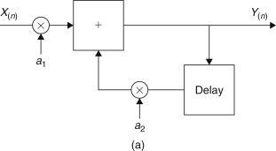
Figure 15.17(b). The arrangement for achieving high-pass filtering and differentiation again requires a single delay element. The output sequence is given by
![]() The filter has no feedback path so it will always be stable. Note that a1=−1 and with a2=0 and a3=1 the structure behaves as a differentiator. These are simple examples of first-order structures and are not necessarily
the most efficient in terms of their use of multiplier or adder resources. Although a second-order system would result if
two first-order structures were run in tandem, full flexibility of second-order IIR structures requires recursive structures.
Perhaps the most common of these emulates the analogue biquad (or twin integrator loop) filter.
The filter has no feedback path so it will always be stable. Note that a1=−1 and with a2=0 and a3=1 the structure behaves as a differentiator. These are simple examples of first-order structures and are not necessarily
the most efficient in terms of their use of multiplier or adder resources. Although a second-order system would result if
two first-order structures were run in tandem, full flexibility of second-order IIR structures requires recursive structures.
Perhaps the most common of these emulates the analogue biquad (or twin integrator loop) filter.
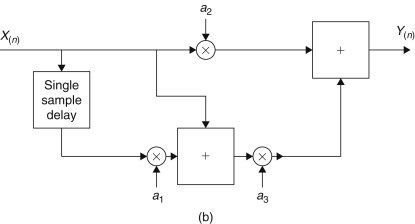
Figure 15.17(c). To achieve the flexibility of signal control, which analogue equalizers exhibit in conventional mixing desks, an IIR filter can be used. Shown here it requires two single-sample value delay elements and six multiplying operations each time it is presented with an input sample value. We have symbolized the delay elements by using the z−1 notation, which is used when digital filter structures are formally analyzed. The output sequence can be expressed as
![]() .The use of z21 notation allows us to express this difference or recurrence equation as
.The use of z21 notation allows us to express this difference or recurrence equation as
![]() . The transfer function of the structure is the ratio of the output over the input, just as it is in the case of an analogue
system. In this case the input and output happen to be sequences of numbers, and the transfer function is indicated by the
notation H(z):
. The transfer function of the structure is the ratio of the output over the input, just as it is in the case of an analogue
system. In this case the input and output happen to be sequences of numbers, and the transfer function is indicated by the
notation H(z):
![]() . Figure 15.17(c): continued: The value of each of the coefficients can be determined from knowledge of the rate at which samples are being
made available, Fs, and your requirement for the amount of cut or boost and of the Q required. One of the first operations is that of prewarping the value of the intended center frequency fc in order to take account of the fact that the intended equalizer center frequency is going to be comparable to the sampling
frequency. The “warped” frequency is given by
. Figure 15.17(c): continued: The value of each of the coefficients can be determined from knowledge of the rate at which samples are being
made available, Fs, and your requirement for the amount of cut or boost and of the Q required. One of the first operations is that of prewarping the value of the intended center frequency fc in order to take account of the fact that the intended equalizer center frequency is going to be comparable to the sampling
frequency. The “warped” frequency is given by
![]() . And now for the coefficients:
. And now for the coefficients:
 The mathematics concerned with filter design certainly appear more complicated than that which is usually associated with
analogue equalizer design. The complication does not stop here though, as a designer must take into consideration the various
compromises brought on by limitations in cost and hardware performance.
The mathematics concerned with filter design certainly appear more complicated than that which is usually associated with
analogue equalizer design. The complication does not stop here though, as a designer must take into consideration the various
compromises brought on by limitations in cost and hardware performance.

The complicated actions of digital audio equalization are an obvious candidate for implementation using infinite impulse response filters and the field has been heavily researched in recent years. Much research has been directed toward overcoming some of the practical problems, such as limited arithmetic resolution or precision and limited processing time. Practical hardware considerations force the resulting precision of any digital arithmetic operation to be limited. The limited precision also affects the choice of values for the coefficients whose value will determine the characteristics of a filter. This limited precision is effectively a processing error, which will make its presence known through the addition of noise to the output. The limited precision also leads to the odd effects for which there is no direct analogue equivalent, such as limit cycle oscillations. The details concerning the structure of a digital filter have a very strong effect on the sensitivity of the filter to noise and accuracy, in addition to the varying processing resource requirement. The best structure thus depends a little on the processing task that is required to be carried out. The skill of the engineer is, as ever, in balancing the factors in order to optimize the necessary compromises.
While complicated filtering is undoubtedly used in digital audio signal processing, spare a thought for the simple process of averaging. In digital signal processing terms this is usually called interpolation (Figure 15.18). The process is used to conceal unrecoverable errors in a sequence of digital sample values and, for example, is used in the compact disc for just this reason.
Figure 15.18. (a) Interpolation involves guessing the value of the missing sample. The fastest guess uses the average of the two adjacent good sample values, but an average based on many more sample values might provide a better answer. The use of a simple rectangular window for including the values to be sampled will not lead to as accurate a replacement value. The effect is similar to that caused by examining the spectrum of a continuous signal that has been selected using a simple rectangular window. The sharp edges of the window function will have frequency components that cannot be separated from the wanted signal. (b) A more intelligent interpolation uses a shaped window that can be implemented as an FIR, or transversal, filter with a number of delay stages, each contributing a specific fraction of the sample value of the output sum. This kind of filter is less likely than the simple linear average process to create audible transitory aliases as it fills in damaged sample values.


15.9. Other Binary Operations
One useful area of digital activity is related to filtering, and its activity can be described by similar algebra. The technique uses a shift register whose output is fed back and combined with the incoming logic signal. Feedback is usually arranged to come from earlier stages as well as the final output stage. The arrangement can be considered as a form of binary division. For certain combinations of feedback the output of the shift register can be considered as a statistically dependable source of random numbers. In the simplest form the random output can be formed in the analogue domain by the simple addition of a suitable low-pass filter. Such a random noise generator has the useful property that the noise waveform is repeated, which allows the results of stimulating a system with such a signal to be averaged.
When a sequence of samples with a nominally random distribution of values is correlated with itself, the result is identical to a band-limited impulse (Figure 15.19). If such a random signal is used to stimulate a system (this could be an artificial reverberation device, an equalizer, or a loudspeaker under test) and the resulting output is correlated with the input sequence, the result will be the impulse response of the system under test. The virtue of using a repeatable excitation noise is that measurements can be made in the presence of other random background noise or interference, and if further accuracy is required, the measurement is simply repeated and the results averaged. True random background noise will average out, leaving a “cleaner” sequence of sample values that describe the impulse response. This is the basis behind practical measurement systems.
Figure 15.19. Correlation is a process in which one sequence of sample values is checked against another to see just how similar both sequences are. A sinusoidal wave correlated with itself (a process called auto correlation) will produce a similar sinusoidal wave. By comparison, a sequence of random sample values will have an autocorrelation function that will be zero everywhere except at the point where the samples are exactly in phase, yielding a band-limited impulse.

Shift registers combined with feedback are also used in error detecting and correction systems.
15.10. Sampling and Quantizing
It is not possible to introduce each element of this broad topic without requiring the reader to have some foreknowledge of future topics. The aforementioned text has tacitly admitted that you will wish to match the description of the processes involved to a digitized audio signal, although we have pointed out that handling audio signals in the digital domain is only an example of some of the flexibility of digital signal processing.
The process of converting an analogue audio signal into a sequence of sample values requires two key operations. These are sampling and quantization. They are not the same operation, for while sampling means that we only wish to consider the value of a signal at a fixed point in time, the act of quantizing collapses a group of amplitudes to one of a set of unique values. Changes in the analogue signal between sample points are ignored. For both of these processes the practical deviations from the ideal process are reflected in different ways in the errors of conversion.
Successful sampling depends on ensuring that the signal is sampled at a frequency at least twice that of the highest frequency component. This is Nyquist’s sampling theorem. Figure 15.20 shows the time domain view of the operation, whereas Figure 15.21 shows the frequency domain view.
Figure 15.20. (a) In the time domain the process of sampling is like one of using a sequence of pulses, whose amplitude is either 1 or 0, and multiplying it by the value of the sinusoidal waveform. A sample and hold circuit holds the sampled signal level steady while the amplitude is measured. (b) At a higher frequency, sampling is taking place approximately three times per sinusoid input cycle. Once more it is possible to see that even by simply joining the sample spikes the frequency information is still retained. (c) This plot shows the sinusoid being under sample, and on reconstituting the original signal from the spikes the best-fit sinusoid is the one shown as the dashed line. This new signal will appear as a perfectly proper signal to any subsequent process and there is no method for abstracting such aliases from properly sampled signals. It is necessary to ensure that frequencies greater than half of the sampling frequency Fs are filtered out before the input signal is presented to a sampling circuit. This filter is known as an antialiasing filter.


Figure 15.21. (a) The frequency domain view of the sampling operation requires us to recognize that the spectrum of a perfectly shaped sampling pulse continues forever. In practice sampling, waveforms do have finite width and practical systems do have limited bandwidth. We show here the typical spectrum of a musical signal and the repeated spectrum of the sampling pulse using an extended frequency axis. Note that even modern musical signals do not contain significant energy at high frequencies and, for example, it is exceedingly rare to find components in the 10-kHz region more than −30 dB below the peak level. (b) The act of sampling can also be appreciated as a modulation process, as the incoming audio signal is being multiplied by the sampling waveform. The modulation will develop sidebands, which are reflected on either side of the carrier frequency (the sampling waveform), with a set of sidebands for each harmonic of the sampling frequency. The example shows the consequence of sampling an audio bandwidth signal that has frequency components beyond F2/2, causing a small but potentially significant amount of the first lower sideband of the sampling frequency to be folded or aliased into the intended audio bandwidth. The resulting distortion is not harmonically related to the originating signal and can sound truly horrid. Use of an antialias filter before sampling restricts the leakage of the sideband into the audio signal band. The requirement is ideally for a filter with an impossibly sharp rate of cutoff, and in practice a small guard band is allowed for tolerance and finite cutoff rates. Realizing that the level of audio signal with a frequency around 20 kHz is typically 60 dB below the peak signal level, it is possible to perform practical filtering using seventh-order filters. However, even these filters are expensive to manufacture and represent a significant design problem in their own right.


15.10.1. Sampling
Practical circuitry for sampling is complicated by the need to engineer ways around the various practical difficulties. The simple form of the circuit is shown in Figure 15.22. The analogue switch is opened for a very short period, tac each 1/Fs seconds. In this short period the capacitor must charge (or discharge) to match the value of the instantaneous input voltage. The buffer amplifier presents this voltage to the input of the quantizer or analogue-digital converter (ADC). There are several problems. The series resistance of the switch sets a limit on how large the storage capacitor can be while the input current requirements of the buffer amplifier set a limit on how low the capacitance can be. The imperfections of the switch mean that there can be significant energy leaking from the switching waveform as the switch is operated and there is the problem of cross talk from the audio signal across the switch when it is opened. The buffer amplifier itself must be capable of responding to a step input and settling to the required accuracy within a small fraction of the overall sample period. The constancy or jitter of the sampling pulse must be kept within very tight tolerances and the switch itself must open and close in exactly the same way each time it is operated. Finally, the choice of capacitor material is itself important because certain materials exhibit significant dielectric absorption.
Figure 15.22. An elementary sample and hold circuit using a fast low distortion semiconductor switch that is closed for a short time to allow a small-valued storage capacitor to charge up to the input voltage. The buffer amplifier presents the output to the quantizer.

The overall requirement for accuracy depends greatly on the acceptable signal-to-noise ratio (SNR) for the process, which is much controlled by the resolution and accuracy of the quantizer or converter. For audio purposes we may assume that suitable values for Fs will be in the 44- to 48-kHz range. The jitter or aperture uncertainty will need to be in the region of 120 pse, acquisition and settling time need to be around 1 μs, and the capacitor discharge rate around 1 V/s for a signal that will be quantized to 16 bits if the error due to that cause is not to exceed +/−0.5 LSB. The jitter performance is complex to visualize completely because of the varying amplitude and frequency component of the jitter itself.
At this stage you will need to be sure you are confident that you appreciate that the combined effect of the antialias filtering and the proper implementation of the sampling process mean that sampled data contain perfectly all of the detail up to the highest frequency component in the signal permitted by the action of the antialias filter.
15.10.2. Quantizing
The sampled input signal must now be measured. The dynamic range that can be expressed by an n-bit number is approximately proportional to 2n and this is more usually expressed in dB terms. The converters used in test equipment such as DVMs are too slow for audio conversion but it is worthwhile considering the outline of their workings (Figure 15.23). A much faster approach uses a successive approximation register (SAR) and a digital-to-analogue converter (DAC) (Figure 15.24).
Figure 15.23. The simplest ADC uses a ramp generator, which is started at the beginning of conversion. At the same time a counter is reset and the clock pulses are counted. The ramp generator output is compared with the signal from the sample and hold and when the ramp voltage equals the input signal the counter is stopped. Assuming that the ramp is perfectly linear (quite difficult to achieve at high repetition frequencies) the count will be a measure of the input signal. The problem for audio bandwidth conversion is the speed at which the counter must run in order to achieve a conversion within approximately 20 μs. This is around 3.2768 GHz and the comparator would need to be able to change state within 150 μs with, in the worst case, less than 150 μV of differential voltage. There have been many developments of this conversion technique for instrumentation purposes.

Figure 15.24. The SAR operates with a DAC and a comparator, initially reset to zero. At the first clock period the MSB is set and the resulting output of the DAC is compared to the input level. In the example given here the input level is greater than this and so the MSB value is retained and, at the next clock period, the next MSB is set. In this example the comparator output indicates that the DAC output is too high, the bit is set to 0, and the next lower bit is set. This is carried out until all of the DAC bits have been tried. Thus a 16-bit ADC would require only 17 clock periods (one is needed for reset) in which to carry out a conversion.

A very simple form of DAC is based on switching currents into a virtual earth summing point. The currents are derived from a R–2R ladder, which produces binary weighted currents (Figure 15.25). The incoming binary data directly controls a solid state switch, which routes a current either into the virtual earth summing point of the output amplifier or into the local analogue ground. Since the voltage across each of the successive 2R resistors is halved at each stage the current that is switched is also halved. The currents are summed at the input to the output buffer amplifier. The limit to the ultimate resolution and accuracy is determined partly by the accuracy of adjustment and matching of the characteristics of the resistors used and also by the care with which the converter is designed into the surrounding circuitry. Implementation of a 16-bit converter requires that all of the resistors are trimmed to within 0.0007% (half of an LSB) of the ideal value and, further, that they all maintain this ratio over the operational temperature of the converter. The buffer amplifier must be able to settle quickly and it must not contribute to the output noise significantly.
Figure 15.25. The basic form of the R–2R digital to analogue (DAG) converter is shown here implemented by ideal current switches. The reference voltage can be an audio bandwidth signal and the DAC can be used as a true four quadrant multiplying converter to implement digitally controlled analogue level and equalization changes. Other forms of switching currents are also used and these may not offer a true multiplication facility.

There are many variations on the use of this technique with one common approach being to split the conversion into two stages. Typically, a 16-bit converter would have the top 8 most significant bits control a separate conversion stage, which sets either the voltage or the current with which the lower 8 LSBs operate. The approach has to contend with the problem of ensuring that the changeover point between the two stages remains matched throughout the environmental range of the converter. One solution to the problem of achieving an accurate binary ratio between successive currents is to use a technique called dynamic element balancing.
Whereas sampling correctly executed loses no information, quantizing inevitably produces an error. The level of error is essentially dependent on the resolution with which the quantizing is carried out. Figure 15.26 illustrates the point by showing a sinusoid quantised to 16 quantizing levels. A comparison of the quantized output with the original has been used to create the plot of the error in the quantizing. The error waveform of this example clearly shows a high degree of structure, which is strongly related to the signal itself. The error can be referred to as quantizing distortion, granulation noise, or simply quantizing noise.
Figure 15.26. The input sinusoid is shown here prior to sampling as a dotted line superimposed on the staircase shape of the quantized input signal. The two’s complement value of the level has been shown on the left-hand edge. The error signal is the difference between the quantized value and the ideal value assuming a much finer resolution. The error signal, or quantizing noise, lies in the range of ±l q. Consideration of the mean square error leads to the expression for the rms value of the quantizing noise:
![]() where q is the size of a quantizing level. The maximum rms signal amplitude that can be described is
where q is the size of a quantizing level. The maximum rms signal amplitude that can be described is
![]() . Together the expression combines to give the expression for SNR(indB):
. Together the expression combines to give the expression for SNR(indB):
![]() .
.

One obvious nonlinearity will occur when the input signal amplitude drops just below the threshold for the first quantizing level. At this stage the quantizing output will remain at zero and all knowledge of the size of the signal will be lost. The remedy is to add a small amount of noise to the signal prior to quantizing (Figure 15.27). This deliberate additional noise is known as dither noise. It does reduce the dynamic range by an amount that depends on its exact characteristics and amplitude but the damage is typically 3 dB. One virtue is that as the original input signal amplitude is reduced below the ±1 quantizing level thresholds (q) the noise is still present and therefore, by virtue of the intrinsic nonlinearity of the quantizer, so are the sidebands that contain vestiges of the original input signal. Thus the quantizer output must also contain information about the original input signal level even though it is buried in the noise. However, the noise is wideband and a spectral plot of the reconstituted waveform will show an undistorted signal component standing clear of the wideband noise.
Figure 15.27(a). Adding a small amount of random noise to the signal prior to quantizing can help disguise the otherwise highly correlated quantizing noise. Aided by the binary modulation action of the quantizer, the sidebands of the noise are spread across the whole audio band width and to a very great degree their correlation with the original distortion signal is broken up. In this illustration the peak-to-peak amplitude of the noise has been set at ±1.5 q.

Figure 15.27(b). The quantizer maps the noisy signal onto one of a range of unique levels as before.
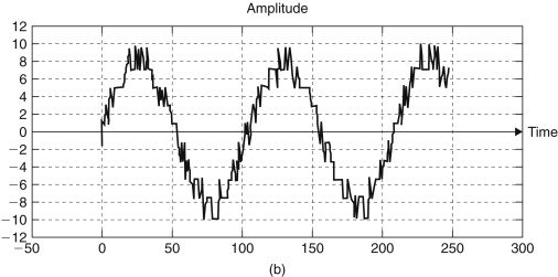
Figure 15.27(c). The resulting quantizing noise can be compared with the original signal and this time you can see that the noise waveform has lost the highly structured relationship shown in Figure 15.26.
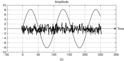
Unfortunately, it is also quite a problem to design accurate and stable quantizers. The problems include linearity, missing codes, differential nonlinearity, and nonmonotonicity. Missing codes should be properly considered a fault since they arise when a converter either does not produce or respond to the relevant code. A suitable test is a simple ramp. A powerful alternative test method uses a sinusoidal waveform and checks the amplitude probability density function. Missing, or misplaced codes, and nonmonotonic behavior can show up readily in such a plot.
Linearity can be assessed overall by using a sinusoidal test signal since the output signal will contain harmonics. The performance of an ADC can be carried out in the digital domain by direct use of the discrete fast Fourier transform. The DAC can be checked by driving it with a computer-generated sequence and observing the output in the analogue domain. The trouble with using the simple harmonic distortion test is that it is not easy to check the dynamic performance over the last decade of bandwidth and for this reason the CCIR twin tone intermodulation distortion is much preferred.
Differential nonlinearity is the random unevenness of each quantization level. This defect can be assessed by measuring the noise floor in the presence of a signal. In a good DAC the rms noise floor should be approximately 95 dB below the maximum rms level (assuming a modest margin for dither). The output buffer amplifier will contribute some noise but this should be at a fixed level and not dependent on the DAC input sample values.
The basic ADC element simply provides an output dependent on the value of the digital input. During the period while a fresh sample is settling, its output can be indeterminate. Thus the output will usually be captured by a sample and hold circuit as soon as the DAC has stabilized. The sample and hold circuit is a zero order hold circuit that imposes its own frequency response on the output signal (Figure 15.28); correction for which can be accommodated within the overall reconstruction filter. The final filter is used to remove the higher components and harmonics of the zero order hold.
Figure 15.28. Finally the DAC output is fed to a zero order hold circuit which performs a similar operation to the sample and hold circuit and then to a reconstruction or output antialiasing filter. The plot of the spectral shape of the zero order hold shows that there are frequency components, at decreasing levels, at harmonic intervals equal to Fs.

15.10.3. Other Forms of ADC and DAC
Flash converters (Figure 15.29) function by using an array of comparators, each set to trigger at a particular quantizing threshold. The output is available directly. These days the technique is most commonly employed directly as shown in digitizing video waveforms. However, there is a use for the technique in high-quality oversampling converters for audio signals.
Figure 15.29. A chain of resistors provides a series of reference voltages for a set of comparators whose other input is the input signal. An 8-bit encoder will need 255 comparators. Their output will drive an encoder that maps the output state of the 255 comparators onto an 8-bit word. The NMINV control line is used to convert the output word from an offset binary count to a two’s complement form. A 16-bit converter would require an impracticably large number of comparators (65536) in addition to posing serious difficulties to setting the 65536 resistor values to the required tolerance value. The technique does have one virtue in speed and in not needing a sample and hold amplifier to precede it.

One great benefit of operating with digital signals is their robustness; they are, after all, construed as either 1 or 0 irrespective of the cable or optical fiber down which they travel. Their disadvantage is that the digital signals do cover a wide bandwidth. Since bandwidth is a valuable resource there has been much effort expended in devising ways in which an apparently high-quality signal can be delivered using fewer bits. The telephone companies were among the first to employ digital compression and expansion techniques but the technology has been used for nontelephonic audio purposes. In the A and i law converters (Figure 15.30), the quantizing steps, q, do not have the same value. For low signal levels the quantizing levels are closely spaced and become more widely spaced at higher input levels. The decoder implements the matching inverse conversion.
Figure 15.30. The relationship between digital input word and analogue output current is not linear. The sign bit is the MSB and the next three bits are used to set the chord slope. The lower 4 bits set the output steps within each chord. The drawing shows the equivalent output for a linear 8-bit DAC.

Another approach to providing a wide coding range with the use of fewer bits than would result if a simple linear approach were to be taken is exemplified in the flying comma or floating point type of converter. In this approach a fast converter with a limited coding range is presented with a signal that has been adjusted in level such that most of the converter’s coding range is used. The full output sample value is determined by the combination of the value of the gain setting and of the sample value returned by the converter. The problem here is that the change in gain in the gain stage is accompanied by a change in background noise level and this too is coded. The result is that the noise floor that accompanies the signal is modulated by the signal level, which produces a result that does not meet the performance requirement for high-quality audio. A more subtle approach is exemplified in syllabic companders. The NICAM approach manages a modest reduction from around 1 Mbs−1 to 7.04 kbs−1 and we see in it an early approach to attempts to adapt the coding process to the psychoacoustics of human hearing.
The encoder will need to have the matching inverse characteristic in order that the net transfer characteristic is unity. The dynamic range of an 8-bit m or A-law converter is around 62 dB and this can be compared to the 48 dB that a linear 8-bit converter can provide. The use of companding (compressing and then expanding the coding range) could be carried in the analogue domain prior to using a linear converter. The difficulty is then one of matching the analogue sections. This is an approach that has been taken in some consumer video equipment.
Delta sigma modulators made an early appearance in digital audio effects processors for a short while. One of the shortcomings of the plain delta modulator is the limitation in the rate at which it can track signals with high slew rates. As we have shown, each pulse is worth one unit of charge to the integrator. To make the integrator climb faster the rate of charge can be increased so that high slew rate signals can be tracked.
Oversampling techniques can be applied to both ADCs and DACs. The oversampling ratio is usually chosen as a power of 2 in order to make computation more efficient. Figure 15.31 shows the idea behind the process for either direction of conversion. The 4× oversampling shown is achieved by adding samples with zero value at each new sample point. At this stage of the process the spectrum of the signal will not have been altered and thus there are still the aliases at multiples of Fs. The final stage is to filter the new set of samples with a low-pass filter set to remove the components between the top of the audio band and the lower sideband of the 4×Fs component.
Figure 15.31(a). The oversampling process adds zero valued dummy samples to the straight sampled signal. If oversampling is being carried out in the DAC direction, then the digital sequence of samples is treated as if these extra dummy samples had been added in. The sequence is then filtered using an interpolation filter, which creates useful values for the dummy samples.
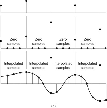
Figure 15.31(b). At the new sample rate (shown here as 4×Fs). The spectrum of the signal now extends to 4×Fs, although there is only audio content up to Fs/2. Thus when the signal is passed to the DAC element (an element that will have to be able to work at the required oversampling speed) the resulting audio spectrum can be filtered simply from the nearest interfering frequency component, which will be at 4×Fs. Note that the process of interpolation does not add information. If the oversampling is being carried out in the ADC direction, the analogue audio signal itself will be sampled and quantized at the higher rate. The next stage requires the reduction of the sequence of data by a factor of four. First data are filtered in order to remove components in the band between the top of the required audio band and the lower of the 4×Fs sideband and then the data sequence can be simply subsampled (only one data word out of each four is retained).

The process effectively transfers the antialias filter from the analogue to the digital domain with the attendant advantages of digital operation. These include a near ideal transfer function, low ripple in the audio band, low group delay distortion, wide dynamic range, exactly repeatable manufacture, and freedom from a wide range of analogue component and design compromises. The four times upsampling process spreads the quantization noise over four times the spectrum, thus only 1/4 of the noise power now resides in the audio band. If we assume that the noise spectrum is uniform and that dither has been judiciously applied, this is equivalent to obtaining a 1-bit enhancement in dynamic range within the audio bandwidth in either digital or analogue domains. This performance can be further improved by the process of noise shaping.
The information capacity of a communication channel is a function of the SNR and the available bandwidth. Thus there is room for trading one against the other. The higher the oversampling ratio, the wider the bandwidth in which there is no useful information. If samples were to be coarsely quantized it should be possible to place the extra quantization noise in part of the redundant spectrum. The process of relocating the noise in the redundant spectrum and out of the audio band is known as noise shaping and it is accomplished using a recursive filter structure (the signal is fed back to the filter). Practical noise shaping filters are high order structures that incorporate integrator elements in a feedback path along with necessary stabilization.
The process of oversampling and noise shaping can be taken to an extreme, and implementation of this approach is available in certain DACs for compact disc systems. The audio has been oversampled by 256× in the Philips bit stream device, 758× in the Technics’ MASH device, and 1024× in Sony’s device. The output is in the form of a pulse train modulated by its density (PDM), by its width (PWM), or by its length (PLM). High oversampling ratios are also used in ADCs, which are starting to appear on the market at the current time.
15.11. Transform and Masking Coders
We indicated very early on that there may be some advantage in terms of the reduction in data rate to taking the Fourier transform of a block of audio data and transmitting the coefficient data. The use of a technique known as the discrete cosine transform is similar in concept and is used in the AC-2 system designed by Dolby Laboratories. This system can produce a high-quality audio signal with 128 kb per channel.
The MUSICAM process also relies on a model of the human ear’s masking processes. The encoder receives a stream of conventionally encoded PCM samples, which are then divided into 32 narrow bands by filtering. The allocation of the auditive significance of the contribution that each band can make to the overall program is then carried out prior to arranging the encoded data in the required format. The principle in this encoder is similar to that planned for the Philips digital compact cassette system.
The exploitation of the masking thresholds in human hearing lies behind many of the proposed methods of achieving bit rate reduction. One significant difference between them and conventional PCM converters is the delay between applying an analogue signal and the delivery of the digital sample sequence. A similar delay is involved when the digital signal is reconstituted. The minimum delay for a MUSICAM encoder is in the region of 9 to 24 ms depending on how it is used. These delays do not matter for a program that is being replayed but they are of concern when the coders are being used to provide live linking program material in a broadcast application.
A second, potentially more damaging, problem with these perceptual encoders is that there has been insufficient work carried out on the way in which concatenations of coders will affect the quality of the sound passing through. Although this problem affects the broadcaster more, the domestic user of such signals may also be affected. Be sure that perceptual coding techniques remove data from the original, as these data cannot be restored. Thus a listener who wishes to maintain the highest quality of audio reproduction may find that the use of his preamplifier’s control or room equalizer provides sufficient change to an encoded signal that the original assumptions concerning masking powers of the audio signal may no longer be valid. Thus the reconstituted analogue signal may well be accompanied by unwelcome noise.
References
There are no numbered references in the text but the reader in search of more detailed reading may first begin with some of the texts listed here. One risk exists in this multidisciplinary field of engineering and that is the rate at which the state-of-the-art of digital audio is being pushed forward. Sometimes it is simply the process of ideas that were developed for one application area (e.g., submarine holography) becoming applicable to high-quality audio processing.
A useful overall text is that of John Watkinson (The Art of Digital Audio, Butterworth-Heinemann, ISBN 0-240-51270-7).
No text covers every aspect of the subject and a more general approach to many topics can be found in the oft-quoted Rabiner and Gold (Theory and Application of Digital Signal Processing, Rabiner and Gold, ISBN 0-13-914-101-4). Although it was initially published in 1975, the principles have not changed, indeed it is salutary to read the book and to realize that so much of what we think of as being modern was developed in principle so long ago.
Undoubtedly the best book to help the reader over the tricky aspects of understanding the meaning of transforms (Laplace, Fourier, and z) is by Peter Kraniauskus (Transforms in Signals and Systems, Addison-Wesley, ISBN 0-201-19694-8).
Texts that describe the psychoneural, physiological, and perceptive models of human hearing can be found in Brian Moore’s tome (An Introduction to the Psychology of Hearing, Academic Press ISBN 0-12-505624-9), and in James Pickles’s An Introduction to the Physiology of Hearing (Academic Press, ISBN 0-12-554754-4). For both of these texts a contemporary publication date is essential as developments in our basic understanding of the hearing progress are still taking place.
Almost any undergraduate text that handles signals and modulation will cover the topic of sampling, quantizing, noise, and errors sufficiently well. A visit to a bookshop that caters for university or college requirements should prove useful.
Without doubt the dedicated reader should avail themselves of copies of the Journal of the Audio Engineering Society in whose pages many of the significant processes involved in digital audio have been described. The reader can achieve this readily by becoming a member. The same society also organizes two conventions each year at which a large number of papers are presented.
Additional sources of contemporary work may be found in the Research Department Reports of the BBC Research Department, Kingswood Warren, UK, while the American IEEE ICASSP proceedings and the related IEEE journals have also held details of useful advances.
[9] Baert, ...Digital audio and compact disc technology 2nd Ed. 1992 Butterworth-Heinemann
[10] Pohlmann K.C., Advanced digital audio 1991 Sams
[11] Pohlmann K.C., Principles of digital audio 2nd Ed. 1989 Sams
[12] Sinclair R., Introducing digital audio 1991 PC Publishing