
Intel® Pentium® Processors
Abstract
This chapter builds on the previous chapter by exploring the Intel(R) Pentium(R) processor family. The chapter begins by looking at the changes introduced by the Intel(R) Pentium(R), Intel(R) Pentium(R) Pro, and Intel(R) Pentium(R) 4 processors. Topics covered include the superscalar execution pipeline, out-of-order execution, μops, and Intel(R) Hyper-Threading. The chapter ends with the extension from 32- to 64-bit processors.
In the previous chapter, the early history of the x86 architecture was introduced. While the early 16-bit processors introduced many of the fundamental principles of the x86 architecture, the Intel® 80386 truly embodies the aspects of what is considered by many developers to be the traditional x86 architecture. Aside from extending the architecture to 32 bits, the 80386 added many of the process isolation and memory protection features that are an integral part of modern operating systems.
The requirements placed on technology increase at a large order of growth, and therefore processor technology must continually improve to support these demands. In the time following the release of the 80386, most of these demands revolved around computational performance. The consumer market was surging with performance-intensive applications, such as 3D games and multimedia, while at the same time the rising availability of the Internet created a demand for infrastructure capable of supporting these new workloads.
This changing technological landscape significantly shaped the processor design of the time. The successor to the 80386, the Intel® 80486, focused on improving the performance of the functionality introduced with the 80386. For example, the floating point coprocessor was integrated directly into the processor, as opposed to requiring a separate chip. Additionally, a memory cache was added to the 80486, reducing the number of accesses to external memory. The Intel® Pentium® processor family redesigned how the execution pipeline of Intel® Architecture operated. This provided significant performance gains without requiring any direct intervention from the programmer.
The rest of this chapter investigates the important changes to Intel Architecture made during this era that affect performance, ranging from the Pentium® to Intel® Pentium® 4 processors.
2.1 Intel® Pentium®
After the 80486, the first of the four, technically five, Intel Pentium processors, shown in Figure 2.1, was introduced in 1993. The name Pentium is derived from the Greek word πέντε (pente), which means five, since the Pentium is the fifth hardware revision, that is, the P5 microarchitecture. Despite this, the Pentium name was also used for later processors that were not based on the P5 microarchitecture.

Whereas the 80486 had a 8-KB cache for storing both code and data, the Pentium had a 16-KB cache, with 8-KB reserved for caching data and 8-KB reserved for caching instructions. Whereas the 80486 achieved instruction-level parallelism (ILP) through instruction pipelining, the Pentium processor was 2-wide superscalar, which significantly improved ILP. The Pentium also introduced MMX™ technology, the first set of Single Instruction Multiple Data (SIMD) extensions to the x86 instruction set.
2.1.1 Superscalar
Prior to the 80486, the predecessor to the Pentium, each instruction was executed serially. In other words, each instruction began and finished execution before the execution of the next instruction could begin. This resulted in inefficient utilization of the processor’s resources, as instruction execution did not require all of those resources simultaneously.
The 80486 introduced the concept of instruction pipelining. Instruction pipelining partitions the execution process into multiple independent steps capable of occurring in parallel. Instructions traverse these partitions one stage at a time. Once an instruction progresses to the next step, the next instruction can take its place in the pipeline, and so on. As a result, the pipeline can simultaneously execute multiple instructions. This leads to better utilization of the processor’s resources, as each instruction only consumes a subset of the total resources. In other words, instruction pipelining provides a finer level of granularity for the allocation of processor resources.
The execution pipeline of the 80486 is partitioned into five stages, meaning that ideally five instructions are executing simultaneously. As the pipeline advances, effective utilization depends on each stage making forward progress to the next stage, with the oldest instruction exiting the pipeline and a new instruction entering the pipeline. A situation where forward progress cannot be made is referred to as a hazard. There are three types of pipeline hazards:
Structural Hazards Two instructions both require the same hardware resource.
Data Hazard Two instructions share a data dependency. For example, one instruction might depend on the result of another instruction.
Control Hazard Instructions within pipeline were speculatively executed but the branch was predicted incorrectly.
When a hazard occurs, the pipeline stalls in order to allow the hazard to pass. This stall is referred to as a bubble in the pipeline, since there is an empty gap introduced.
The Pentium processor increased the ILP of the 80486’s instruction pipeline even further. Whereas the 80486 had one pipeline capable of executing five instructions simultaneously, the i586 architecture had two pipelines each capable of executing five instructions simultaneously. This is referred to as multiple issue, because multiple instructions are ideally entering and exiting the pipeline at each step. In order to accommodate this, the Pentium processor adds duplicate execution units to support the second pipeline.
The number of instructions the processor can issue each cycle is referred to as the processor’s width, so the Pentium processor is described as 2-wide. It is important to understand that the two pipelines are not identical. As a result, there are restrictions on which instructions can be issued together. If any of these restrictions are violated, then only one instruction can be issued. This decision, whether to issue one or two instructions, is performed automatically in hardware during execution. Therefore, the Pentium processor is classified as a dynamic multiple issue processor, that is, superscalar. This is opposed to a static multiple issue processor, where the programmer and compiler are responsible for scheduling instructions to obey the restrictions.
2.2 Intel® Pentium® Pro
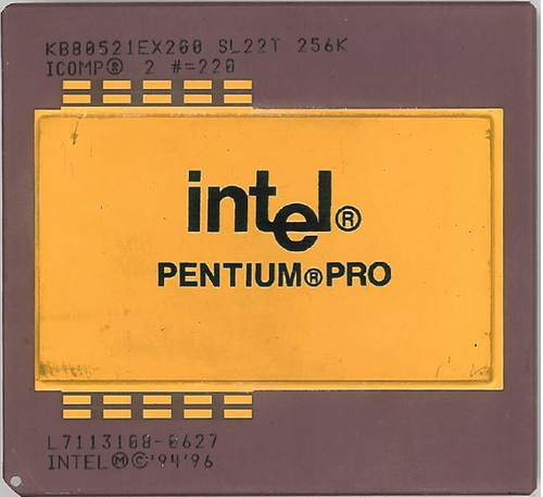
After the first Pentium, the Intel Pentium Pro, shown in Figure 2.2, was introduced in 1995. The Pentium Pro was the first processor to utilize the new P6 architecture, that is, the i686. The P6 architecture introduced a significant number of improvements to the first Pentium, and therefore remained a staple of the Pentium lineup, until the introduction of the NetBurst architecture with the Pentium 4.
Whereas the 80486 and first Pentium processor only contained one memory cache on-die, the Pentium Pro added a second, larger but slower, cache. This cache is known as the second level cache or L2 cache. Additionally, the introduction of the Physical Address Extensions (PAE) increased the amount of usable physical memory from 4-GB to 64-GB. The Pentium Pro also brought improvements to the execution pipeline, introducing out-of-order execution and μops, and by extending the processor’s width to 3-wide superscalar.
2.2.1 PAE
The PAE increase the number of the processor’s physical address pins, expanding the size of the physical address space. It is important to understand that this change only extends the physical address space, not the linear or logical address spaces. With PAE enabled, pointers are still 32 bits in length and each process can still only map up to 4-GB worth of pages at the same time. The benefit is that the processor can address more memory, and therefore more pages can be kept resident in memory, rather than being swapped to and from slow storage, simultaneously.
Remember from Section 1.4.2 that traditional 32-bit paging utilizes one page directory table, with entries capable of either mapping a 4-MB page or referencing a page table, and a set of page tables, with entries mapping 4-KB pages. Both the page directory and page tables are 4-KB in size, with 1024 32-bit entries.
In order to accommodate the extended physical memory region when PAE is enabled, the entries in both types of tables are extended from 32 to 64 bits. Accounting for the reserved and configuration bits, these 64-bit entries are capable of handling a maximum of 52 physical address pins, that is, 4-PB; however, this is limited by the number of the processor’s physical address pins. Starting with the Pentium Pro, the number of pins was increased from 32 to 36, increasing the physical address space to 64-GB, 236.
While the size of each entry doubled, the size of the different tables was not increased, so the number of entries in each table is reduced from 1024 to 512. As a result, a page table spans 2-MB of the linear address space, 4096 × 512, instead of 4-MB. Therefore, with PAE enabled a PDE maps a 2-MB page instead of a 4-MB page. Additionally, the linear address coverage of the page directory table shrinks from 4-GB to 1-GB, (1024 × 1024 × 2) × 512, meaning that one page directory is no longer sufficient to cover the entire linear address space. Therefore, another level is added to the paging hierarchy, known as the page directory pointer table (PDPT). The PDPT has four 64-bit entries that each point to a page directory.
2.2.2 μops
Processor architectures are classified as either a Reduced Instruction Set Computer (RISC) or as a Complex Instruction Set Computer (CISC). The difference between the two classifications is that RISC architectures have a small number of simple general purpose instructions that each perform one single operation, essentially providing the basic building blocks for computations. CISC architectures, on the other hand, have a large number of more complex instructions, that are each capable of performing multiple internal operations.
For example, consider performing an arithmetic operation on a value in memory. For a RISC architecture, the corresponding arithmetic instruction would only be capable of operating on a register. As a result, before the operation could begin, a load instruction would be issued to fetch the value from memory and store it into a register. Once that is complete, the operation would be performed, with the result stored in a register. Finally, a store instruction would be issued to commit the result back to memory. On the other hand, the arithmetic operation’s instruction for a CISC architecture would accept a memory operand. Assuming the memory operand is the instruction’s destination operand, this form of the instruction would automatically fetch the value from memory, perform the operation, and then commit the result back to memory, all in one instruction.
As a result, CISC architectures are often able to perform an algorithm in less instructions than a RISC architecture, since one CISC instruction can perform the equivalent work of multiple RISC instructions. On the other hand, due to the simplified nature of their instructions, RISC architectures are often less complex, and therefore require less silicon. Additionally, due to the logical separation of different instructions for specific tasks, RISC architectures are capable of scheduling and executing instructions at a finer granularity than CISC architectures.
The x86 family of processors are classified as CISC, since x86 instructions are capable of performing multiple internal operations. Starting with the Pentium Pro, Intel Architecture is actually a hybrid approach between the two. The instruction set is not modified, so x86 instructions are still CISC, but the Front End of the processor translates each instruction into one or more micro-ops, typically referred to as μops or sometimes just uops. These μops are very similar to RISC instructions, each specialized for a specific task.
Consider the previous example for how CISC and RISC architectures handle an arithmetic operation. The x86 instruction set still supports memory operands for that arithmetic instruction, making it appear CISC to the programmer; however, the Front End might decode that single instruction into three μops. The first, a load μop, might be responsible for loading the contents described by the memory operand. The second μop would then be responsible for performing the actual operation. The third μop would then be responsible for committing the result back to memory.
This hybrid approach gives Intel Architectures the benefits of both approaches. Since memory accesses can be expensive, fetching fewer instructions benefits performance. The CISC nature of the x86 instruction set can be thought of as opcode compression, thereby improving instruction fetch bandwidth. At the same time, by breaking these complex instructions into smaller μops, the execution pipeline can be more agile and flexible, as Section 2.2.3 describes.
The cost of this approach is a more complicated Front End, which requires logic for decoding instructions into μops. In general, this cost is insignificant compared to the performance improvement achieved.
2.2.3 Out-of-Order Execution
As discussed in Section 2.1.1, prior to the 80486, the processor handled one instruction at a time. As a result, the processor’s resources remained idle while the currently executing instruction was not utilizing them. With the introduction of pipelining, the pipeline was partitioned to allow multiple instructions to coexist simultaneously. Therefore, when the currently executing instruction had finished with some of the processor’s resources, the next instruction could begin utilizing them before the first instruction had completely finished executing. The introduction of μops expanded significantly on this concept, splitting instruction execution into smaller steps.
Each type of μop has a corresponding type of execution unit. The Pentium Pro has five execution units: two for handling integer μops, two for handling floating point μops, and one for handling memory μops. Therefore, up to five μops can execute in parallel. An instruction, divided into one or more μops, is not done executing until all of its corresponding μops have finished. Obviously, μops from the same instruction have dependencies upon one another so they can’t all execute simultaneously. Therefore, μops from multiple instructions are dispatched to the execution units.
Taking advantage of the fine granularity of μops, out-of-order execution significantly improves utilization of the execution units. Up until the Pentium Pro, Intel processors executed in-order, meaning that instructions were executed in the same sequence as they were organized in memory. With out-of-order execution, μops are scheduled based on the available resources, as opposed to their ordering. As instructions are fetched and decoded, the resulting μops are stored in the Reorder Buffer. As execution units and other resources become available, the Reservation Station dispatches the corresponding μop to one of the execution units. Once the μop has finished executing, the result is stored back into the Reorder Buffer. Once all of the μops associated with an instruction have completed execution, the μops retire, that is, they are removed from the Reorder Buffer and any results or side-effects are made visible to the rest of the system. While instructions can execute in any order, instructions always retire in-order, ensuring that the programmer does not need to worry about handling out-of-order execution.
To illustrate the problem with in-order execution and the benefit of out-of-order execution, consider the following hypothetical situation. Assume that a processor has two execution units capable of handling integer μops and one capable of handling floating point μops. With in-order scheduling, the most efficient usage of this processor would be to intermix integer and floating point instructions following the two-to-one ratio. This would involve carefully scheduling instructions based on their instruction latencies, along with the latencies for fetching any memory resources, to ensure that when an execution unit becomes available, the next μop in the queue would be executable with that unit.
For example, consider four instructions scheduled on this example processor, three integer instructions followed by a floating point instruction. Assume that each instruction corresponds to one μop, that these instructions have no interdependencies, and that all three execution units are currently available. The first two integer instructions would be dispatched to the two available integer execution units, but the floating point instruction would not be dispatched, even though the floating point execution unit was available. This is because the third integer instruction, waiting for one of the two integer execution units to become available, must be issued first. This underutilizes the processor’s resources. With out-of-order execution, the first two integer instructions and the floating point instruction would be dispatched together.
In other words, out-of-order execution improves the utilization of the processor’s resources. Additionally, because μops are scheduled based on available resources, some instruction latencies, such as an expensive load from memory, may be partially or completely masked if other work can be scheduled instead.
Register Renaming
From the instruction set perspective, Intel processors have eight general purpose registers in 32-bit mode, and sixteen general purpose registers in 64-bit mode, however, from the internal hardware perspective, Intel processors have many more registers. For example, the Pentium Pro has forty registers, organized in a structure referred to as a Physical Register File.
While this many extra registers might seem like a performance boon, especially if the reader is familiar with the performance gain received from the eight extra registers in 64-bit mode, these registers serve a different purpose. Rather than providing the process with more registers, these extra registers serve to handle data dependencies in the out-of-order execution engine.
When a value is stored into a register, a new register file entry is assigned to contain that value. Once another value is stored into that register, a different register file entry is assigned to contain this new value. Internal to the processor core, each data dependency on the first value will reference the first entry, and each data dependency on the second value will reference the second entry. Therefore, the out-of-order engine is able to execute instructions in an order that would otherwise be impossible due to false data dependencies.
2.3 Intel® Pentium® 4
The P6 microarchitecture was used as the basis for the Intel® Pentium® Pro, Intel® Pentium® II, and Intel® Pentium® III processor families. As a result, each of these generations mostly focused on improving the performance of the previous generation while adding new instructions. On the other hand, the Pentium 4, shown in Figure 2.3, was based on the NetBurst architecture. This new architecture adds new features including IA-32e mode, which extends the processor from 32-bits to 64-bits, and Intel® Hyper-Threading.

2.3.1 IA-32e Mode
The IA-32e processor mode extends Intel Architecture from 32-bit to 64-bit. In order to enter IA-32e mode, the processor must be in protected mode with PAE enabled. Paging is also a requirement for IA-32e mode, so the 64-bit page tables must be be constructed prior to transitioning into the new mode. In IA-32e mode, a fourth level is added to the paging hierarchy, the page map level 4 (PML4) table. This 4-KB table contains 512 entries that point to PDPTs. Each PDPT is extended from 4 entries to 512 entries. Also, unlike 32-bit paging, where a PDPTE could only reference a page directory table, a PDPTE can map a 1-GB page. Once the CR3 register holds the physical base address of the PML4 table, the LME bit in the IA32_EFER MSR is set and then paging is enabled.
Similar to the extension from 16-bit to 32-bit, the extension from 32-bit to 64-bit is handled through the addition of another bit in the code segment descriptor, the L bit. If the L bit is set, then the code within that segment operates in 64-bit mode. If the L bit is not set, but the processor is in IA-32e mode, then the segment operates in compatibility mode. This allows for 16-bit and 32-bit applications to still run while the processor is in 64-bit mode. If the L bit is not set and the D bit is not set, then the code within that segment operates in 16-bit mode. If the L bit is not set and the D bit is set, then the code within that segment operates in 32-bit mode.
In 64-bit mode, the memory address size and the long integer size is increased from 32-bit to 64-bit. While pointers are 64-bit, and are therefore theoretically capable of addressing up to 16 exabytes, 264, supporting such a large address space introduces extra complexity for little gain. As a result, at the time of this writing, 64-bit processors that support a full 64-bit address space are uncommon. Instead, these processors support a more manageable subset of the full address space. The size of the physical and linear address space supported by the processor can be accessed through /proc/cpuinfo. For example:
In this example, the processor supports a physical address space of 64-GB, and a linear address space of 256-TB. At the time of this writing, 36 physical address pins are common for consumer hardware. On the other hand, server hardware, such as Intel® Xeon® processors, often support a significantly larger physical address space, for example, 46 physical address pins. In order to prevent a 64-bit memory address from exceeding the supported linear address space, the processor will fault on an address that doesn’t follow canonical form. The canonical address form requires that all bits outside of the implemented address range all have the same value as the most significant bit of the supported linear address space. In the example above, the linear address space supports 48 bits, bits 0 through 47, so bits 48 through 63 must be set to the same value as bit 47.
Additionally, enabling 64-bit mode adds eight more general purpose registers, R8 through R15, increasing the total from eight to sixteen registers. The SIMD vector registers are also increased from eight to sixteen. Also, aside from the FS and GS segment registers, which are used for thread-local storage, segmentation is only supported in flat mode.
2.3.2 Multi-Core
Until this point, the main granularity of hardware parallelism was the processor die. For the best parallel performance, multiple processors are installed into special motherboards that contain multiple processor sockets. With this configuration, all of the processors can either share the same memory, or each processor socket can be configured to have its own set of corresponding memory DIMM slots. In the case where each processor has a separate set of memory DIMMs installed, memory is divided into two categories. For a given processor, the memory installed in that socket’s corresponding DIMM slots are known as local memory. On the other hand, all of the other memory is known as nonlocal memory or remote memory. Memory that is local to a specific processor provides the fastest accesses, while remote memory provides slower accesses, due to the distance between the processor and the memory. Because of this disparity between the memory performance of local and remote memory, this is referred to as a Non-Uniform Memory Access (NUMA) configuration.
In order to best utilize these expensive hardware resources, the operating system needs to be aware of the system topology. For example, without this knowledge, the kernel might inadvertently allocate memory on the slow remote memory while the fast local memory is still available. In Linux, the kernel is configured for NUMA configurations by grouping memory resources into zones. These zones control what regions of memory are given priority, and allow for customization of different memory policies.
While these multiprocessor configurations provide the best performance, and are still popular in the server and workstation segments, these configurations tend to be expensive and require extensive system tuning.
In order to provide better parallel performance than a single processor, without requiring an expensive multiple processor configuration, some of the Pentium 4 models duplicated the processor’s execution resources into multiple processor cores. Each core operates as a separate logical processor contained within the processor package.
Within a multi-core processor’s die, resources are divided into two categories: core and uncore resources. Core resources are duplicated for each logical processor. On the other hand, uncore resources are shared between all of the cores present on that processor die. As one would expect, there are tradeoffs in performance between parallel and serial workloads for designing resources to be either core or uncore.
The coordination of multiple cores occurs in an identical fashion to multiple processors. After a hardware #RESET, one of the logical processors, which can be either a core or separate processor, is selected as the boot processor. The boot processor is responsible for performing the system initialization by executing the early BIOS code. All of the other logical processors halt and wait for the boot processor to bring them online. Once the boot processor has completed initialization, it uses Inter-Processor Interrupts (IPIs) to wake the application processors.
2.3.3 Intel® Hyper-Threading
Intel Hyper-Threading Technology adds additional parallelism into each processor core by dividing it into multiple hardware threads. Whereas multiple processor cores duplicate all of the core resources for each core, hardware threads only require the duplication of a small subset of execution state. Typically, this subset only includes the registers and APIC.
Since only the execution state is duplicated, but not the execution pipeline, the core’s execution pipeline is shared between each hardware thread. As a result, μops from both hardware threads are present within the core’s execution pipeline simultaneously. In other words, Hyper-Threading allows the μop scheduler to fill underutilized execution pipeline resources by interleaving the μops of two different processes.
Within Linux, each hardware thread appears as a separate logical processor. For instance, one quad-core processor with Hyper-Threading will register eight logical processors. The CONFIG_SCHED_SMT Kconfig option enables additional logic within the Linux kernel scheduler that makes it aware of hardware threads. Using this information, it can make better decisions when migrating processes between logical processors.