
Early Intel® Architecture
Abstract
This chapter is the first of three that explores the Intel(R) Architecture, focusing on the fundamental design. The chapter begins with the Intel(R) 8086, the first x86 processor. Then the Intel(R) 8087 coprocessor is covered, along with the IEEE 754 floating point specification and the Intel(R) 80286. The chapter ends by looking at the Intel(R) 80386, the first 32-bit Intel(R) processor and the first processor to run Linux.
The power button is pressed, causing the #RESET pin to be asserted, that is, the voltage is driven into the predefined threshold that represents the active state logic level. After a predefined number of clock cycles pass, the #RESET pin is then deasserted, invoking the hardware reset. The hardware reset is responsible for initializing the processor to a known state. This includes setting the registers, including the general purpose, control and status registers, to their documented initial values.
This first “breath” leaves the processor in an execution state significantly different from the one which most developers are familiar. The processor begins execution in 16-bit Real-Address mode. This journey between 16-bit Real-Address mode and 64-bit, or 32-bit, Protected Virtual-Address mode occurs every time the processor is powered on. In doing so, this process mirrors the historical evolution of the Intel® Architecture, from the 16-bit 8086 of 1978 to the 64-bit Intel® Core™ processor family of the twenty-first century. As the computer is booted, more than 40 years of advancements in processor technology unfold in the blink of an eye.
The author imagines that some readers are wondering what benefit could possibly come from the retention of all these relics of computing antiquity in modern processor design. Backwards compatibility, which by definition involves maintaining older designs, directly benefits the reader. As readers, hopefully, continue through this book, they will find references to many architectural features. Education on and usage of these features is an investment of the reader’s time. By strictly maintaining backward compatibility, Intel ensures that the investments made by the reader today continue to pay dividends for the foreseeable future. Consider that original bytecode compiled in the late 1970s will still run unmodified on a modern Intel® processor fabricated in 2014.
Other detractors argue that Intel Architecture is inelegant. Since elegance is in the eyes of the beholder, this claim is hard to refute. The author is not a hardware engineer; however, as a software engineer, the author sees an interesting parallel between hardware and software in this claim. Many software projects are architected to be elegant solutions to a well-defined problem. This elegance erodes over time as new features, which were unimaginable during the design phase, are requested and bug fixes and workarounds are introduced. After enduring these unavoidable harsh realities of the software lifecycle, a software’s worth comes not from elegance, but from whether that software still works, is still reliable, and can still be extended to meet future needs. The author submits that x86 still works, is still reliable, and can still be extended.
Covering every aspect of Intel Architecture would require an entire book, as opposed to a couple of chapters. The goal of the next three chapters is to introduce the fundamentals of the architecture, in order to provide just enough knowledge to enable the reader to understand the later content in this book, as well as begin to reason effectively about power consumption and performance.
Because Intel Architecture has been in a constant state of evolution for the last 40 years, and has been steadily increasing in complexity, the author has divided the introduction to Intel Architecture into three separate chronologically ordered chapters, sampling the general timeline of Intel products. Despite following the timeline, history is only being used as a convenient tool. Not all processors or architectural details will be covered in the sections that follow. Also, unless explicitly stated, not all technologies are discussed in the section corresponding to the processor that introduced them. Instead, each section will utilize the given processor as a vehicle for simplifying and explaining important concepts of the modern x86 architecture. This has the dual benefit of gradually introducing the concepts of the modern x86 architecture in a natural and logical progression, while also providing the context necessary to understand the reasoning behind the technical decisions made through the years.
This chapter examines some of the earliest members of the x86 family. The majority of these processors are 16-bit. The chapter ends with the first 32-bit x86 processor, and the first processor to run Linux, the Intel® 80386.
1.1 Intel® 8086
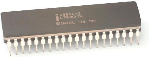
The 8086, introduced in 1978 and shown in Figure 1.1, was not the first processor developed by Intel, however it was the first processor to implement what would be known as the x86 architecture. In fact, the two digits in the name x86 correspond to the fact that the first x86 processor designations all ended with 86, such as 8086, 80186, 80286, 80386, and so on. This trend was continued by Intel until the Pentium® processor family. Despite being introduced in 1978, the 8086 was continually produced throughout the 1980s and 1990s. Famously, NASA had been using the 8086 in their shuttles until 2011.
In stark contrast to the thousands of pages in the modern Intel® Software Developer Manual (SDM), the 8086 user manual, including a full reference on the system behavior, programming tools, hardware pinout, instructions and opcodes, and so on, fits within about two hundred pages. This simplified nature makes the 8086 an excellent introduction to the fundamental concepts of the x86 architecture. The rest of this book will build further on the concepts introduced here.
In the architecture of the 8086, there are three fundamental design principles (Intel Corporation, 1979). The first principle is the usage of specialized components to isolate and distribute functionality. In other words, rather than one large monolithic system architecture, building an 8086 system provided flexibility in the peripherals selected. This allowed system builders to customize the system to best accommodate the needs of the given situation. The second principle is the inherent support for parallelism within the architecture. At the time of the 8086, this parallelism came in the form of combining multiple processors and coprocessors together, in order to perform multiple tasks in parallel. The third principle was the hierarchical bus organization, designed to support both complex and simple data flows.
To illustrate these principles, consider that along with the 8086, there were two other Intel processors available, the 8088 and 8089. The 8088 was an identical processor to the 8086, except that the external data bus was 8 bits, instead of 16 bits. The 8088 was chosen by IBM® for the heart of the “IBM compatible PC.” The 8089 was a separate coprocessor, with it’s own instruction set and assembler, designed for offloading data transfers, such as Direct Memory Access (DMA) requests. Interestingly, the 8089 was not chosen by IBM® for the “IBM compatible PC,” and therefore was never widely adopted.
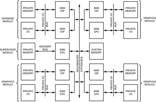
One or more of each of these chips could be mixed and matched, along with a selection of peripherals, to provide systems highly tailored for software requirements. For example, consider the system diagram in Figure 1.2. This diagram, taken from the 8086 User Manual, demonstrates a multiprocessor configuration consisting of one primary 8086 processor, along with three 8088 processors, driving three graphics peripherals, and five 8089 processors, with three accelerating I/O to the graphics peripherals and two accelerating access to a database.
This modularity can be seen throughout the design of the 8086. For example, the internal architecture of the 8086 is cleanly divided into two categories: the execution unit (EU), and the bus interface unit (BIU). The EU contains all of the resources for maintaining and manipulating the internal processor state, including the CPU registers and arithmetic/logic unit (ALU). The EU, however, is unable to access the system’s memory, which requires usage of the system bus. The BIU is solely responsible for interfacing with the system bus. This separation allows for the two units to operate in parallel, with the BIU fetching data over the bus while the EU is executing instructions.
To accommodate this asynchronous nature, the two units interface with an instruction queue, therefore allowing the BIU to prefetch instructions before they are required. When the BIU detects that there is an available slot in the queue, it begins to fetch an instruction to fill that slot. When the EU detects that there is a valid entry in the queue, it removes that entry and begins executing it. If the EU requires the evaluation of a memory operand, it passes the effective address to the BIU, which suspends instruction prefetching and retrieves the desired system information.
Beginning to understand the x86 architecture starts with the realization that a processor is simply a state machine with states, described by the contents of memory and the registers, and inputs that transition between different states, the instruction set.
1.1.1 System State
For the general case, there are three members of the 8086 storage hierarchy: the processor’s registers, the system’s external memory, that is, RAM, and persistent storage, that is, the disk drive. The registers provide fast volatile storage located very close to the processor on the die. Since this memory is very fast, it is also very expensive, and therefore very scarce. On the other hand, the volatile external memory is significantly cheaper than the registers, and therefore more prevalent than the registers, but is also orders of magnitude slower. Similarly, the persistent storage is significantly cheaper than the external memory, and therefore is available in greater quantities, but is also orders of magnitude slower than external memory. To quantify the inverse relationship between storage density and speed, consider that the 8086 might be paired with a 10 MB hard drive, was capable of addressing 1 MB of external RAM, and had seven 16-bit registers.
Address space
The 8086 is comprised of two different address spaces, the memory address space, capable of addressing 1 MB, and the I/O address space, capable of addressing 64 KB.
External peripherals can either be mapped into the I/O address space or memory-mapped. Device registers in the I/O address space are manipulated with the IN and OUT instructions, while memory-mapped device registers can be manipulated with general purpose instructions, just like external memory.
In order to address 1 MB of memory with a 16-bit processor, which would normally be limited to 216 bytes of memory, the 8086 utilizes a technique referred to as segmentation. Segmentation divides the memory space into four 64 KB segments. The definition of the segments is completely up to the programmer to control. There are no restrictions on their configuration. For instance, nothing prevents segments from overlapping.
A segmented address, referred to as a logical address, is comprised of two components, a segment selector and an offset. The segment selector takes the form of a segment register. The offset is a 16-bit pointer, which represents the displacement of the address from the segment’s base address. Since the 16-bit offset is unsigned, an overflow or underflow results in a wrap around effect within the segment. Therefore, the offset can be considered modulo the segment.
For the 8086, there are four segments: (0) the code segment, described by the CS segment selection register, (1) the stack segment, described by the SS segment register, (2) the data segment, described by the DS segment register, and (3) the extra data segment, described by the ES segment register. Some instructions imply the usage of a specific segment. For instance, instructions that manipulate the stack imply the stack segment and instruction fetches imply the code segment. In other cases, the segment register will need to be explicitly provided, or the default segment register will need to be overridden.
The EU only handles logical addresses, with address translation from logical to physical being handled by the BIU. In order to translate a logical address into a 20-bit physical address, the segment register is logically shifted left by 4 bits, which is equivalent to multiplying by 16, and then added to the offset.
1.1.2 Registers
Aside from the four segment registers introduced in the previous section, the 8086 has seven general purpose registers, and two status registers.
The general purpose registers are divided into two categories. Four registers, AX, BX, CX, and DX, are classified as data registers. These data registers are accessible as either the full 16-bit register, represented with the X suffix, the low byte of the full 16-bit register, designated with an L suffix, or the high byte of the 16-bit register, delineated with an H suffix. For instance, AX would access the full 16-bit register, whereas AL and AH would access the register’s low and high bytes, respectively.
The second classification of registers are the pointer/index registers. This includes the following four registers: SP, BP, SI, and DI, The SP register, the stack pointer, is reserved for usage as a pointer to the top of the stack. The SI and DI registers are typically used implicitly as the source and destination pointers, respectively. Unlike the data registers, the pointer/index registers are only accessible as full 16-bit registers.
As this categorization may indicate, the general purpose registers come with some guidance for their intended usage. This guidance is reflected in the instruction forms with implicit operands. Instructions with implicit operands, that is, operands which are assumed to be a certain register and therefore don’t require that operand to be encoded, allow for shorter encodings for common usages. For convenience, instructions with implicit forms typically also have explicit forms, which require more bytes to encode. The recommended uses for the registers are as follows:
BX Data (relative to DS)
CX Loop counter
DX Data
SI Source pointer (relative to DS)
DI Destination pointer (relative to ES)
SP Stack pointer (relative to SS)
BP Base pointer of stack frame (relative to SS)
Aside from allowing for shorter instruction encodings, this guidance is also an aid to the programmer who, once familiar with the various register meanings, will be able to deduce the meaning of assembly, assuming it conforms to the guidelines, much faster. This parallels, to some degree, how variable names help the programmer reason about their contents. It’s important to note that these are just suggestions, not rules.
Additionally, there are two status registers, the instruction pointer and the flags register.
The instruction pointer, IP, is also often referred to as the program counter. This register contains the memory address of the next instruction to be executed. Until 64-bit mode was introduced, the instruction pointer was not directly accessible to the programmer, that is, it wasn’t possible to access it like the other general purpose registers. Despite this, the instruction pointer was indirectly accessible. Whereas the instruction pointer couldn’t be modified through a MOV instruction, it could be modified by any instruction that alters the program flow, such as the CALL or JMP instructions.
Reading the contents of the instruction pointer was also possible by taking advantage of how x86 handles function calls. Transfer from one function to another occurs through the CALL and RET instructions. The CALL instruction preserves the current value of the instruction pointer, pushing it onto the stack in order to support nested function calls, and then loads the instruction pointer with the new address, provided as an operand to the instruction. This value on the stack is referred to as the return address. Whenever the function has finished executing, the RET instruction pops the return address off of the stack and restores it into the instruction pointer, thus transferring control back to the function that initiated the function call. Leveraging this, the programmer can create a special thunk function that would simply copy the return value off of the stack, load it into one of the registers, and then return. For example, when compiling Position-Independent-Code (PIC), which is discussed in Chapter 12, the compiler will automatically add functions that use this technique to obtain the instruction pointer. These functions are usually called __x86.get_pc_thunk.bx(), __x86.get_pc_thunk.cx(), __x86.get_pc_thunk.dx(), and so on, depending on which register the instruction pointer is loaded.
The second status register, the EFLAGS register, is comprised of 1-bit status and control flags. These bits are set by various instructions, typically arithmetic or logic instructions, to signal certain conditions. These condition flags can then be checked in order to make decisions. For a list of the flags modified by each instruction, see the Intel SDM. The 8086 defined the following status and control bits in EFLAGS:
Zero Flag (ZF) Set if the result of the instruction is zero.
Sign Flag (SF) Set if the result of the instruction is negative.
Overflow Flag (OF) Set if the result of the instruction overflowed.
Parity Flag (PF) Set if the result has an even number of bits set.
Carry Flag (CF) Used for storing the carry bit in instructions that perform arithmetic with carry (for implementing extended precision).
Adjust Flag (AF) Similar to the Carry Flag. In the parlance of the 8086 documentation, this was referred to as the Auxiliary Carry Flag.
Direction Flag (DF) For instructions that either autoincrement or autodecrement a pointer, this flag chooses which to perform. If set, autodecrement, otherwise autoincrement.
Interrupt Enable Flag (IF) Determines whether maskable interrupts are enabled.
Trap Flag (TF) If set CPU operates in single-step debugging mode.
1.1.3 Instructions
Continuing the scenario described in the introductory section, once the #RESET pin is asserted and deasserted, the processor initializes the program registers to their predefined values. This includes the predefined value of the instruction pointer, providing the BIU the first location to fetch and decode for the execution unit.
This first location is always the last 16 bytes in the physical address space. For a 16-bit processor with 20-bit physical addresses, this is 0xFFFF0. This provides just enough room for a JMP to the BIOS’s real initialization code.
To understand the reasoning behind this, consider that the very first instructions executed, which are responsible for initializing the system and preparing a standardized execution environment before booting the operating system, belong to the BIOS. The BIOS is mapped into the physical address space, but it doesn’t reside in physical memory. Instead, the BIOS is stored in a ROM chip, located on the motherboard, connected with a Low Pin Count (LPC) Bus. This ROM is memory mapped at the very top of the physical address space, such that the last byte of the ROM is at the very top. Therefore, differently sized ROMs have different starting addresses within memory. For example, a 1-KB ROM would start at 0xFFFFF − 0x400 + 1 = 0xFFC00, where as 4-KB ROM would start at 0xFFFFF − 0x1000 + 1 = 0xFF000. These first instructions executed, the last bytes of the BIOS ROM, are the only address guaranteed to contain valid BIOS code, and since it belongs to the BIOS, it is guaranteed to know where in physical memory the rest of the initialization code resides.
From this point on, the processor continues its loop of fetching new instructions, decoding those instructions, and then executing those instructions. Each instruction defines an operation that transitions the state machine from one state to another.
Each individual instruction is comprised of one or more forms, that is, various encodings handling different operand types. An operand is simply a parameter for the instruction, defining what aspect of the state should be acted upon. Examples of operands include a specific register, memory address, or an immediate, that is, a constant value at the time of assembly. As mentioned earlier, operands can be either explicit or implicit.
To illustrate this, consider the ADD instruction, which at the time of the 8086, had six unique forms. These forms are listed in Table 1.1. Notice how the first five forms are explicit, whereas the last form has an implicit operand, AX.
Table 1.1
Forms for the ADD Instruction on the Intel® 8086
| Operand Form | Example | Note |
| register, register | add %ax, %dx | dx = ax + dx |
| register, memory | add %ax, (%dx) | *(short *)dx = *(short *)dx + ax; |
| memory, register | add (%dx), %ax | ax = ax + *(short *)dx; |
| immediate, register | add $10, %ax | ax = ax + 10; |
| immediate, memory | add $10, (%bx) | *(short *)bx = *(short *)bx + 10; |
| immediate | add $10 | ax = ax + 10; |
The 8086 had an instruction set comprising of about one hundred unique instructions, not accounting for different forms. These instructions can be divided into five logical groupings. For a full reference of the available instructions, along with their meanings and operands, see the Intel SDM.
Data movement
The first group contains instructions that move data from one operand to another. This includes instructions like MOV, which can move data from one operand to another, PUSH and POP, which pushes an operand onto the stack or pops the top of the stack into the operand, and XCHG, which atomically swaps the contents of two operands.
Integer arithmetic
The second group contains instructions that perform integer arithmetic. This includes instructions that perform the standard familiar arithmetic operations, such as ADD, SUB, MUL, and DIV.
Additionally, x86 supports instructions for performing these operations “with carry” or “with borrow.” This is used for implementing these operations over an arbitrarily large number of bytes. In the case of a carry, the bit in EFLAGS is preserved for the next instruction to interpret. For example, each ADC, add with carry, instruction uses this bit to determine whether the result should be incremented by one, in order to borrow the bit carried from the previous ADC operation.
Typically each of these instructions sets the relevant status bits in the EFLAGS register. This often obviates the need to issue an explicit comparison instruction for some checks, like checks for zero, or less than zero. Instead, the flag can simply be reused from the arithmetic operation.
As mentioned earlier, the AX register is designated the accumulator register, so most arithmetic instructions have implicit forms that perform operations on, and store the result in AX.
Boolean logic
The third group contains instructions that perform boolean logic. This includes instructions like AND, which only sets bits in the result that are set in both operands, OR, which only sets bits in the result that are set in at least one of the operands, and XOR, which only sets bits in the result that are set in one operand and not the other.
Similar to the arithmetic group, these instructions also favor AX for their results. Additionally, they set the same bits in EFLAGS, sans the carry bits.
Flow control
The fourth group contains instructions that modify the program flow. Unlike a high level language, there are no if statements or for loop constructs. Instead, arithmetic and logical instructions set bits in the EFLAGS register, which can then be acted upon by control flow instructions. For example, consider the following two equivalent code snippets:

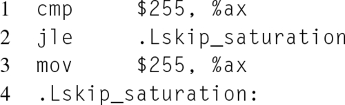
In the assembly version, the CMP instruction checks the contents of the register operand, AX, against an immediate, that is, a constant at assemble time, and sets the status flags in the EFLAGS register accordingly. While the JMP instruction unconditionally performs the jump, there are also conditional jump instructions. These instructions take the form of Jcc, where cc is a condition code. A condition code represents a predefined set of one or more conditions based on the status of EFLAGS. For example, the JNZ instruction only performs the jump if the Zero Flag (ZF) is not set. In the listing above, the JLE instruction only jumps to .Lskip_saturation when AX is less than or equal to 255, thereby skipping the saturation that occurs on line 3.
String
The fifth group contains instructions designed to operate on strings. This includes instructions for loading, LODS, storing, STOS, searching, SCAS, and comparing, CMPS, strings.
The string instructions are designed to heavily utilize implicit operands. The current character, either being loaded from, stored to, or scanned for, is held in AX. The source and destination pointers to strings are stored in DS:SI and ES:DI, respectively. The length of the strings are typically held in CX.
For example, the LODS instruction loads the byte at DS:SI into the AX register and then decrements or increments, depending on the status of the direction flag in EFLAGS, SI. Conversely, the STOS instruction stores the byte in AX into the memory location ES:DI, and then updates the pointer accordingly.
The SCAS instruction compares the value of AX to the byte located at the memory location pointed to by ES:DI, updates the EFLAGS register accordingly, and then autoincrements or autodecrements DI. The CMPS instruction, designed for fast string comparison, compares the bytes located at ES:DI and DS:SI, updates the EFLAGS register, and then autoincrements or autodecrements both DI and SI.
While these string instructions perform one stage of their respective operations, they can be extended to perform the full operation by combining them with the REP prefix. This prefix repeats the instruction until the given condition is satisfied. This condition is specified through the suffix of the REP prefix. Table 1.2 lists the available REP prefixes and their subsequent meanings.
Table 1.2
Meanings of the REP Prefix (Intel Corporation, 2013)
| Prefix | Meaning |
| REP | Repeat until CX = 0 |
| REPE/REPZ | Repeat until EFLAGS.ZF != 0 |
| REPNE/REPNZ | Repeat until EFLAGS.ZF == 0 |
1.1.4 Machine Code Format
One of the more complex aspects of x86 is the encoding of instructions into machine codes, that is, the binary format expected by the processor for instructions. Typically, developers write assembly using the instruction mnemonics, and let the assembler select the proper instruction format; however, that isn’t always feasible. An engineer might want to bypass the assembler and manually encode the desired instructions, in order to utilize a newer instruction on an older assembler, which doesn’t support that instruction, or to precisely control the encoding utilized, in order to control code size.
8086 instructions, and their operands, are encoded into a variable length, ranging from 1 to 6 bytes. To accommodate this, the decoding unit parses the earlier bits in order to determine what bits to expect in the future, and how to interpret them. Utilizing a variable length encoding format trades an increase in decoder complexity for improved code density. This is because very common instructions can be given short sequences, while less common and more complex instructions can be given longer sequences.
The first byte of the machine code represents the instruction’s opcode. An opcode is simply a fixed number corresponding to a specific form of an instruction. Different forms of an instruction, such as one form that operates on a register operand and one form that operates on an immediate operand, may have different opcodes. This opcode forms the initial decoding state that determines the decoder’s next actions. The opcode for a given instruction format can be found in Volume 2, the Instruction Set Reference, of the Intel SDM.
Some very common instructions, such as the stack manipulating PUSH and POP instructions in their register form, or instructions that utilize implicit registers, can be encoded with only 1 byte. For instance, consider the PUSH instruction, that places the value located in the register operand on the top of the stack, which has an opcode of 010102. Note that this opcode is only 5 bits. The remaining three least significant bits are the encoding of the register operand. In the modern instruction reference, this instruction format, “PUSH r16,” is expressed as “0x50 + rw” (Intel Corporation, 2013). The rw entry refers to a register code specifically designated for single byte opcodes. Table 1.3 provides a list of these codes. For example, using this table and the reference above, the binary encoding for PUSH AX is 0x50, for PUSH BP is 0x55, and for PUSH DI is 0x57. As an aside, in later processor generations the 32- and 64-bit versions of the PUSH instruction, with a register operand, are also encoded as 1 byte.
Table 1.3
Register Codes for Single Byte Opcodes “+rw” (Intel Corporation, 2013)
| rw | Register |
| 0 | AX |
| 1 | CX |
| 2 | DX |
| 3 | BX |
| 4 | SP |
| 5 | BP |
| 6 | SI |
| 7 | DI |
If the format is longer than 1 byte, the second byte, referred to as the Mod R/M byte, describes the operands. This byte is comprised of three different fields, MOD, bits 7 and 6, REG, bits 5 through 3, and R/M, bits 2 through 0.
The MOD field encodes whether one of the operands is a memory address, and if so, the size of the memory offset the decoder should expect. This memory offset, if present, immediately follows the Mod R/M byte. Table 1.4 lists the meanings of the MOD field.
Table 1.4
Values for the MOD Field in the Mod R/M Byte (Intel Corporation, 2013)
| Value | Memory Operand | Offset Size |
| 00 | Yes | 0 |
| 01 | Yes | 1 Byte |
| 10 | Yes | 2 Bytes |
| 11 | No | 0 |
The REG field encodes one of the register operands, or, in the case where there are no register operands, is combined with the opcode for a special instruction-specific meaning. Table 1.5 lists the various register encodings. Notice how the high and low byte accesses to the data group registers are encoded, with the byte access to the pointer/index classification of registers actually accessing the high byte of the data group registers.
Table 1.5
Register Encodings in Mod R/M Byte (Intel Corporation, 2013)
| Value | Register (16/8) |
| 000 | AX/AL |
| 001 | CX/CL |
| 010 | DX/DL |
| 011 | BX/BL |
| 100 | SP/AH |
| 101 | BP/CH |
| 110 | SI/DH |
| 111 | DI/BH |
In the case where MOD = 3, that is, where there are no memory operands, the R/M field encodes the second register operand, using the encodings from Table 1.5. Otherwise, the R/M field specifies how the memory operand’s address should be calculated.
The 8086, and its other 16-bit successors, had some limitations on which registers and forms could be used for addressing. These restrictions were removed once the architecture expanded to 32-bits, so it doesn’t make too much sense to document them here.
For an example of the REG field extending the opcode, consider the CMP instruction in the form that compares an 16-bit immediate against a 16-bit register. In the SDM, this form, “CMP r16,imm16,” is described as “81 /7 iw” (Intel Corporation, 2013), which means an opcode byte of 0x81, then a Mod R/M byte with MOD = 112, REG = 7 = 1112, and the R/M field containing the 16-bit register to test. The iw entry specifies that a 16-bit immediate value will follow the Mod R/M byte, providing the immediate to test the register against. Therefore, “CMP DX, 0xABCD,” will be encoded as: 0x81, 0xFA, 0xCD, 0xAB. Notice that 0xABCD is stored byte-reversed because x86 is little-endian.
Consider another example, this time performing a CMP of a 16-bit immediate against a memory operand. For this example, the memory operand is encoded as an offset from the base pointer, BP + 8. The CMP encoding format is the same as before, the difference will be in the Mod R/M byte. The MOD field will be 012, although 102 could be used as well but would waste an extra byte. Similar to the last example, the REG field will be 7, 1112. Finally, the R/M field will be 1102. This leaves us with the first byte, the opcode 0x81, and the second byte, the Mod R/M byte 0x7E. Thus, “CMP 0xABCD, [BP + 8],” will be encoded as 0x81, 0x7E, 0x08, 0xCD, 0xAB.
1.2 Intel® 8087
Unlike the 8086, the 8087, shown in Figure 1.3, wasn’t a standalone processor, but a coprocessor, similar to the 8089. But unlike the 8089, which accelerated I/O operations, the 8087 was developed to accelerate mathematical operations. Notice that in the instructions described in the previous section, all mathematical operations operate only on integers. As a result, all computations involving real numbers needed to be manually implemented in software. Unfortunately, this resulted in a suboptimal situation where the quality, accuracy, and functionality of available software math libraries varied greatly, thus impeding the ability of software to aid in tasks involving real numbers.

To remedy this situation, the 8087 was designed to consolidate as much of the common and error-prone computations into hardware as possible, freeing software engineers to focus on their application’s calculations, rather than on implementing low level math routines. These features include floating point operations, numeric conversions, and common functions, such as the trigonometric and square root functions.
1.2.1 IEEE 754 Floating Point
Intel recognized, as they were beginning development of the 8087, that a standardized floating point format, to be used from then on for all future architecture generations, was required. By standardizing the format, developers would be able to perform numerical analysis of their algorithms once, rather than repeatedly for each hardware generation. Also, once adoption of the new standard had taken hold, developers would be freed from writing custom code for each vendor’s floating point solution, thus increasing software portability.
In order to accomplish this, Intel worked closely with the IEEE committee responsible for developing a standardized format for binary floating point arithmetic, the IEEE 754 standard. This standard, along with the international IEC 559:1989 standard, which is identical in content, defines the floating point format and arithmetic behavior, as well as the minimum precision and environment required for a compliant implementation. The original IEEE 754 format was finalized in 1985 and remained unchanged for twenty-three years, until the standard was extended in 2008. The 2008 revision to the standard retained most of the 1985 standard, and thus its content, along with the design of the 8087, still govern the format and behavior of floating point computations today, as of 2014. It is still important to note that, despite the fact that the standard did much to improve the situation of floating point portability and consistency, the standard does not guarantee that different systems will produce identical results.
Because the full 754 standard wasn’t finalized until 1985, and the 8087 was released in 1980, the 8087 doesn’t technically implement the full standard. Despite this, the 8087 implemented the current draft at the time of its release and both the hardware and Intel played an important role in the development of the standard. Notably, Dr. William Kahan, who was on the IEEE committee and is an expert in numerical analysis, was contracted by Intel to help design the 8087. The author recommends the reader visit Dr. Kahan’s faculty website at Berkeley, located at http://www.eecs.berkeley.edu/~wkahan/, and read some of his publications on the rationale and history behind the standard, and on accuracy and error analysis in floating point computations.
Unlike an unsigned or signed 16-bit integer, which only allows for the representation of whole numbers between [0,216 − 1] or [−215,215 − 1] respectively, floating point allows for the representation of real numbers, as well as very large and small numbers beyond the integer limits. As the name implies, floating point utilizes scientific notation, which decomposes a number into a signed significand and a signed exponent. For example, the number 0.0005 would be represented as 5.0 × 10⁻⁴.
However, using scientific notation introduces a problem, which is that the same number can be represented in multiple ways. For example, 5000.0 × 100, 500.0 × 101, and 5.0 × 10³ are all the same number. Obviously, this could be problematic when comparing two floating point numbers. In order to remedy this, floating point requires that the scientific notation format is normalized. A number in normalized scientific notation has only a single nonzero digit before the decimal point. So in the previous example, 5.0 × 10³ would be the normalized format.
Up to this point, all of the previous examples of scientific notation have been in base 10, hence the × 10x component, however, all floating point numbers assume a base of 2. In order to encode a fraction in the significand in binary, each bit, n, represents ![]() . Because of the normalized binary format, it’s unnecessary to physically represent the leading bit of the significand. Therefore, this bit is implied and an extra bit of precision is gained. The exception to this case, 0, is handled with a reserved exponent of 0.
. Because of the normalized binary format, it’s unnecessary to physically represent the leading bit of the significand. Therefore, this bit is implied and an extra bit of precision is gained. The exception to this case, 0, is handled with a reserved exponent of 0.
Formats, precision, and environment
The IEEE 754 standard defines four floating point types: basic single, basic double, extended single, and extended double. Compliance to the standard requires providing at least one basic type. The single type, corresponding to the float C type, is 32 bits, reserving 24 bits, 23 physical bits plus the implied leading bit, for the significand and 8 bits for the exponent. The double type, corresponding to the double C type, is 64 bits, providing 53 bits, 52 physical bits plus the implied leading bit, for the significand and 11 bits for the exponent. The MSb of each format is the sign bit for the significand.
For the extended types, the standard provides only the minimum length requirements. The single extended type is required to be at least 43 bits, with at least 32 bits for the significand and at least 11 bits for the exponent. The double extended type, corresponding to the long double C type, is required to be at least 79 bits, with at least 64 bits for the significand and 15 bits for the exponent. The bit encoding for the extended types is defined to be implementation-dependent.
One of the goals of the IEEE 754 format was to enable fast floating point sorting that could be performed by the regular integer ALU. One challenge to achieving this goal was how to handle the exponent component, since with a two’s complement encoding extra logic would be needed to compare numbers based on their exponent’s sign. In order to remedy this, a bias was introduced to the exponent component. A bias is simply an offset, added to the exponent, that ensures that the smallest possible value is expressed as all zeros, while the largest possible exponent is expressed as all ones. Because the bias is directly related to the number of elements that can be encoded, and therefore the number of bits in the representation, the bias varies with regards to the type. The standard defines the bias of a single basic type to be 127 and the bias of a double basic type to be 1023. Typically, the notation used for differentiating between biased and unbiased exponents is e and E, respectively.
The largest and smallest exponents, all ones and all zeros, are reserved for encoding special numbers. The largest exponent, e = 255 for floats and e = 2047 for doubles, is reserved for the encoding of infinity, both positive and negative according to the sign bit, and NaN, that is, Not A Number. Infinity is represented by a zero significand while NaN is represented by a nonzero significand. Infinity is designed to represent an edge of representable values, but is designed to compare properly with other numbers. NaNs are the result of an invalid operation and are designed to allow for errors to slowly propagate, which may be acceptable in some situations, as opposed to early termination of the computation with an exception. To accommodate both use cases, there are two types of NaNs, signaling and quiet, with the difference being that signaling NaNs generate an exception.
The smallest exponent, e = 0, is reserved for representing values for which the implicit leading bit in the significand does not apply. The obvious case for this is zero, which is represented by a zero exponent and a zero significand. As mentioned previously, floating point numbers are normalized; however, a special case exists for numbers too small for the standard format. These types of numbers are known as denormals, and are represented with e = 0, and the significand set to the relevant fraction.
In order to promote consistency in computations, the IEEE 754 standard also specifies four user-selectable rounding modes:
Round to Nearest The default rounding mode. As the name suggests, rounds to the closest representable number in the destination’s format.
Round to Zero Always round toward zero.
Round to Negative Infinity Always round down toward negative infinity.
Round to Positive Infinity Always round up toward positive infinity.
In the case of certain conditions, floating point exceptions can be signaled either through the setting of a status flag or with the generation of a signal that invokes a trap handler. There are five defined exceptions:
Invalid Operation Raised when the requested computation cannot be performed. If no trap handler is specified, the result is a NaN.
Division by Zero If no trap handler is specified, the result is infinity.
Overflow If no trap handler is specified, the result is rounded based on the current rounding mode.
Underflow Same behavior as overflow
Inexact Raised when the rounding of a result is unable to be precisely represented or results in an overflow.
C99 support
Extensive support for the functionality described in this section is available in the C programming language, as of the C99 language revision. For a full reference, see Annex F of the C99 specification, along with section 5.2.4.2.2, which describes the characteristics of the format, and section 7.6, which describes access to the floating point environment. Another useful reference is the contents and man pages for the fenv.h, float.h, and math.h header files.
1.2.2 x87 Floating Point
Unlike the 8086, the 8087 exposes its registers as a stack, instead of flat registers. Each of these eight registers is 80 bits in length, and thus each value is internally stored and computed in a double extended format. Values from memory, or the 8086’s registers, are converted from integers, floats, and doubles into this 80-bit format when they are pushed onto the stack. Computations are then performed either with values from the stack or from memory locations. Unlike a traditional stack, each register is also directly addressable as a register relative to the top of the stack. The top of the stack is designated as the ST or ST(0) register. Subsequent registers are designated with an index offset from the top of stack, such as ST(1), ST(2), and so on.
Usage of a stack makes the FPU operate much like a Reverse Polish Notation calculator. For example, in order to add two numbers, they could both be pushed onto the stack before executing an FADD instruction. This instruction will pop both numbers off of the stack, perform the addition operation and push the result onto the stack.
A stack was chosen for the registers as it is intuitive for mathematical operations, like RPN, and accommodates one operand instructions. Using the FXCH instruction, two stack registers can be swapped, and thus the stack registers could be utilized in a fashion that simulates flat registers (Kahan, 1990).
Aside from the stack registers, the 8087 also had a 16-bit status register, a 16-bit tag register, and a 16-bit control register. The status register for the FPU is similar to the EFLAGS register for the CPU. The first 6 bits correspond to the five IEEE 754 exceptions that can be raised during a computation, plus an additional bit to indicate a denormalized operand. Additional entries include 3 bits dedicated to the index of the current register at the top of the stack, 4 bits for expressing condition codes, that is, codes similar to the flags in EFLAGS that are used for comparisons and branches, and a bit representing an interrupt request. The tag register, with 2 bits per stack register, stores the status of the stack register. Each register can be marked as either having a valid entry, an entry of zero, a special reserved number, or as being empty. The control register allows for the masking and unmasking of exception interrupts, as well as control of the rounding mode and precision mode.
Similar to the parallel architecture of the 8086, the 8087 is also divided into two components. The first component, the control unit (CU), is responsible for handling instructions and memory operands, and remains synchronized with the main processor, and thus mirrors the BIU of the 8086. The second component, the numeric execution unit (NEU), is responsible for performing actual computations, and thus mirrors the EU of the 8086. While the floating point unit (FPU), the 8087, was executing a floating point instruction, the CPU was free to execute general purpose instructions, thus providing parallelism to improve performance.
The 8087 and subsequent coprocessors remained separate chips until the 80486 processor, which integrated the FPU into the CPU. While later processor introduced features like MMX™ technology, SSE, and Intel® Advanced Vector Extensions (Intel® AVX), which are also capable of floating point operations, the x87 FPU is still heavily utilized in areas where additional precision is needed.
1.3 Intel® 80286 and 80287
After the 8086 and 80186, the 80286 was introduced in 1982. What makes the 80286 worthy of mention is that it was the first x86 processor designed for multitasking. Much of this multitasking support came through the addition of a memory protection scheme designed to isolate tasks from one another.
Up until this point, no memory protection existed for x86, meaning that every byte in the address space was treated equally, regardless of whether it belonged to the operating system or a user application. This meant that there was no mechanism to prevent a user application from tampering with the code and data of another application or of the operating system. Obviously, this was less than optimal for security, for application isolation, or for operating system constraints on application behavior. To remedy this, the 80286 included an on-chip Memory Management Unit (MMU), which was responsible for transparently translating between logical, that is, segmented addresses consisting of a segment selector and offset, and physical addresses, and for enforcing memory protection. Therefore, each process on the system could be isolated in a separate address space.
1.3.1 Protected and Real Mode
Because this represented a paradigm shift in the processor’s programming model, the two models were split into two separate processor modes. The legacy mode, which was utilized by the 8086 and 80186, was called Real-Address mode, or simply real mode. The new MMU mode with memory protections was called Protected Virtual-Address mode, or simply protected mode. To retain compatibility with legacy applications for the 8086 and 80186, the processor booted into real mode, ensuring that these applications would see the 80286 as simply a faster and better 8086. Applications that wished to take advantage of the features in the new model would boot into real mode and then switch into protected mode. This technique, making new software request new features, is a common trend in x86 for making disruptive changes to the architecture while retaining backwards compatibility.
Transitioning from real mode to protected mode is a fairly straightforward process. The first step is to create and load all of the protected mode memory structures, so that the protected environment operates correctly immediately after the switch. Secondly, the PE bit in the first control register, CR0, is set, which effectively enters protected mode. Finally, a jump instruction is performed to flush any processor caches. At this point, the processor is now executing in protected mode and any new functionality can be utilized. Once protected mode was entered, there was no method for returning to real mode, without resetting the processor.
The 80286 introduced the concept of a privilege level, ranging from level 0, which had the most privileges, to level 3, which had the least. These privilege levels were enforced by the MMU, which wouldn’t permit a task operating at a lesser privilege level to access a memory region marked at a greater privilege level. Four levels were provided in order to provide fine level of control for operating systems that desired it. For example, an operating system’s core functionality might run at privilege level 0, the kernel drivers at level 1, the user space drivers at level 2, and user applications at level 3. This privilege system is part of modern x86, although the Linux kernel only utilizes level 0, for kernel space, and level 1, for user space.
1.3.2 Protected Mode Segmentation
Support for these memory protected regions meant that the current segmentation memory model had to be extended. Originally, segments had been fixed in size; however, that made memory protection more cumbersome, since the fixed sizes were too large for fine grained task control. In order to solve this, segments in protected mode were now of variable size. All of these changes, combined with additional changes designed to allow for the implementation of advanced features, such as swapping, simply wouldn’t work within the confines of the existing segment register format. To accommodate this, the segment register format and behavior in protected mode is completely different from the segment register format and behavior in real mode.
Remember that originally the segment registers simply contained a base address that was shifted and added to the offset to produce a larger address size. In this new model, the segment registers needed more room for the accounting required to support these new features. Therefore, in protected mode only, segments now didn’t reference the base address of the segment, but instead pointed to a descriptor entry in a table of segment descriptors. Each 8-byte entry in this table describes the 24-bit base address, 16-bit size, and 8 bits for the privilege and access information, which is used for marking segments as read only, executable, and so on. The remaining 16 bits store the segment selector, which when loaded into the 16-bit segment register effectively load the segment. To improve performance, by avoiding the need to touch memory each time a segment operation needs to be checked, the other 48 bits of the segment descriptor are cached in a hidden register when the segment selector is loaded.
In order to make segmentation usable for both the operating system and user applications while still enforcing memory protections, two segment descriptor tables exist. The global descriptor table (GDT) is a table of segment descriptors that the operating system, privilege level 0, controls, while the local descriptor table (LDT) is controlled by the user application. Two registers, the GDTR and LDTR, exist for storing the base address of these tables. The global and local descriptor registers are loaded and stored with the LGDT and SGDT, and LLDT and SLDT instructions, respectively. Each segment selector has a special bit indicating whether the descriptor is located in the local or global table.
Each segment descriptor also had a present bit, indicating whether the corresponding segment was currently loaded into memory. If the segment descriptor was loaded into a segment selector register and the present bit in the descriptor was not set, the user program would be paused and an exception would be raised, giving the operating system a chance to load the relevant segment into memory from disk. Once the segment had been loaded, the user program would be resumed. All of this occurred transparently to the user program, and thus provided an early form of hardware supported virtual memory swapping. With swapping, more virtual memory could be allocated by the operating system than was physically available on the computer.
1.3.3 Task Control
Since the processor is only capable of running one application at a time, the job of a multitasking operating system is to provide the illusion that the processor can run multiple tasks at once. Whereas in a single-tasking operating system each job runs from start to completion before moving to next job, a multitasking operating system divides the processor time across each of the required jobs. This switching has to occur quickly and smoothly enough that it is transparent to the user applications, and appears that the processor is running all of the tasks concurrently.
The action of switching the processor from running one process to running a different process is referred to as a context switch. In order to perform a context switch, the operating system must keep track of the full execution state of the processor, including the contents of the registers and memory, for each executing task. On a context switch, the process which was running is paused and the contents of the execution state are saved into storage, while the execution state of the next process to run is loaded from storage into the processor.
The process of determining which process should be run and for how long is referred to as process scheduling. Process scheduling is a well researched problem in computer science that attempts to address many concerns, such as fairness in scheduling or balancing response time with throughput, for many different types of situations involving different numbers of processes with different performance requirements. As such, processor scheduling is a fairly large field, which won’t be discussed in detail within this book. At the time of this writing, most of the processor scheduling research for Linux revolves around optimally scheduling tasks to complement current power-saving techniques. For a good introduction to the fundamental concepts and algorithms, the author recommends Modern Operating Systems by Andrew Tanenbaum.
The 80286 introduced a new feature that allowed for context switches to be handled automatically in hardware. This was facilitated through a special segment, a task state segment. Within the task state segment, all of the execution state for a process is preserved. By issuing a JMP, CALL instruction, or returning from an interrupt, where the destination is the processes’ TSS descriptor, a context switch automatically occurs. The execution state of the currently executing process is automatically copied into the relevant section of the TSS. Once this is complete, the new execution environment, of the process being switched to, is automatically loaded into the processor, and execution of the new process can continue from where it had been previously paused.
Despite full support for context switches in hardware, Linux performs all of its context switches manually with software. This has been done for performance reasons, because the hardware context switch loads and validates all of the execution state, whereas Linux has historically performed some of the loads lazily and optimized some loads based on what actually needs to be restored.
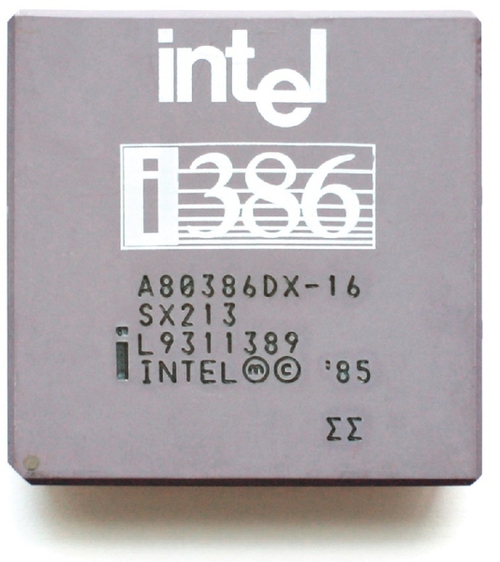
1.4 Intel® 80386 and 80387
After the 80286, the 80386, shown in Figure 1.4, was introduced in 1985, and was continually produced by Intel, by popular demand, until September 2007. The 80386 was the first 32-bit processor in the x86 family, and also expanded many of the fundamental concepts introduced in the 80286. Perhaps even more importantly, since this book focuses on Linux, the 80386 was the first processor that ran Linux. In fact, 80386 support existed in the kernel until it was removed in 2012 (Molnar, 2012). To quote the original Usenet post from Linus Torvalds describing the Linux project:
“I’m doing a (free) operating system (just a hobby, won’t be big and professional like gnu) for 386(486) AT clones. …It uses every conceivable feature of the 386 I could find, as it was also a project to teach me about the 386. (Torvalds, 1991)”
Whereas the 80286 introduced the real and protected processor modes, the 80386 introduced an additional mode. This mode, Virtual 8086 mode, was designed to address the fact that the 80286 did not allow returning to real mode from protected mode, and thus there was previously no way to run legacy and modern applications side by side. Virtual 8086 mode is a special mode designed to be entered from protected mode. This allows for the processor to execute 8086 programs, that is, programs written for real mode, from protected mode. Linux supports Virtual 8086 mode, with CONFIG_VM86, for certain drivers and legacy applications that need to access real mode.
1.4.1 32-Bit Mode
Having already been familiarized with the 16-bit ISA of the early x86 processors, the transition from 16 to 32 bits is straightforward. In 32-bit mode, both memory addresses and integers are extended from 16 to 32 bits, that is, sizeof(int) = sizeof(void *) = 4 bytes. This increases the physical address space to 4-GB, 232. The extended general purpose registers are prefixed with a letter E. For instance, the 16-bit AX register extends to the 32-bit EAX register. The previous register names operate on a subset of the corresponding extended registers. For instance, the AX register references the least significant word of EAX, and the AH and AL registers reference the two least significant bytes of EAX.
In Real-Address mode, everything continues operating exactly as it had before. All instructions in Real-Address mode default to their 16-bit versions. Within protected mode, a new bit was added to the segment descriptors, known as the default bit, or D-bit. When this bit is clear, instructions within the code segment default to 16-bit mode. When this bit is set, instructions within the code segment default to 32-bit mode.
While this bit controls the default size for a given segment, the mode of an individual instruction can override the default size with a special instruction prefix. This prefix, 0x66, is known as the Operand-size override prefix. By using this prefix, it is possible to execute 16-bit instructions in 32-bit Protected Virtual-Address mode, and to even execute 32-bit instructions in 16-bit Real-Address mode.
Aside from adding this new instruction prefix, the 80386 also extends the machine code format. These additions include support for 32-bit immediates, 32-bit displacements, and a new addressing format. As mentioned in Section 1.1.4, there were previously some restrictions on how memory operands could be addressed. These restrictions limited addressing to a base, contained within either the SI, DI, BX, or BP registers, and an optional displacement. Additionally, if the base was stored in SI or DI, an optional offset, also known as an index, could be encoded in BX or BP.
In 32-bit mode, the base and offset encodings in the Mod R/M byte are no longer limited to this subset of general purpose registers. Instead, any general purpose register can be used for either the base or index. In order to accommodate some of these encodings, a new optional byte, the scale-index-base (SIB) byte, may need to follow the MOD R/M byte.
The two most significant bits within the SIB byte encode the scaling factor. A value of zero encodes a scaling factor of one, a value of one encodes a scaling factor of two, a value of two encodes a scaling factor of four, and a value of three encodes a scaling factor of eight. The next 3 bits encode the register containing the index, which is scaled and then added to the base. The last 3 bits, the three least significant bits, encode the register containing the base. Both the index and base registers are encoded using the same values as in the Mod R/M byte for the 8086, as shown in Table 1.5.
In other words, 32-bit x86 memory operands are expressed as:
The result of this calculation, which can be obtained with the LEA instruction, is referred to as the effective address. In AT&T assembly syntax, this is formatted as displacement(base, index, scale). Because LEA can perform up to two additions and a multiplication, and doesn’t modify any flags, it has historically been used as an optimization for general purpose integer arithmetic; however, on modern x86, this is no longer a fruitful optimization.
To illustrate this concept, consider how to load the ith element of an array of integers foo[]. Assume that the index, i, is stored in the ECX register, that the base address of foo[] is stored in the EAX register, and that the desired destination of the contents of foo[i] is the EBX register. Accessing foo[i] translates to the following pointer arithmetic:
Since each element of foo[] is an integer, sizeof(foo[0]) = 4, the ith element could be loaded into EBX with:
The next element, i + 1, could be loaded either by incrementing ECX or by adding a displacement of four:
1.4.2 Paging
Up to this point, memory address translations have occurred in one phase, logical, that is, a segmented address consisting of a segment selector and an offset, to a physical address. The 80286 extended segmentation in order to accommodate the needs of rapidly advancing operating system designs. The design of the 80386 recognized that segmentation alone was not enough to meet these needs, and therefore paging was introduced.
With paging, memory address translations occur in two separate phases. In the first phase, the logical address is converted to a linear address, through the translation method for segmentation. In the second phase, the linear address, produced in the first phase, is converted to a physical address, through the translation method for paging. Notice that paging doesn’t replace segmentation, but instead was designed to complement it.
In a system that implements paging, the address space is divided into multiple pages. A page is simply a fixed-size chunk of memory, which may or may not be currently present in memory. The available physical memory of the system is divided into page frames. A page frame is a memory region capable of holding a page in memory. As required, various pages are swapped in and out of the physical page frames.
Mappings are created between the linear and physical address space through a hierarchical memory structure comprising of multiple tables, referred to as page tables. The page tables are divided into multiple levels, with each level representing pages of a different size. Each entry in the page tables can either map a page of the current size, or reference another table, which can then either map a page of a smaller size or reference another table, and so on.
In the classic x86 paging mode present in the 80386, the page tables are divided into two levels, the page directory and a set of page tables. Each entry in the first level, known as a page directory entry (PDE), can either map a 4-MB page or reference one of the second level page tables. Each entry in the page tables, known as a page table entry (PTE), maps a 4-KB page. The page directory table and each of the page tables are the size of a 4-KB page, meaning that each consists of 1024 entries of 4-B pointers. Therefore, only one page directory table is required to cover the whole 4-GB linear address space, since 1024 ×4-MB = 4-GB. The base physical address of this page directory table is stored in the CR3 register. Additionally, the 1024 entries in each page table cover the 4-MB region that would otherwise be mapped by the corresponding PDE, since 1024 × 4096 = 4-MB.
When a PDE or PTE maps a page, it points to the beginning of either a 4-MB or 4-KB page, so the entry pointer is guaranteed to be at least page aligned. The page directory and page tables are also required to be page aligned. As a result, the bottom 12 bits of the PDE and PTE are guaranteed to be zero, by definition. Rather than wasting these bits, they are used to encode the page’s protection information, whether the page is currently present in memory, and whether the pointer maps a page or references another table. Within these 12 bits are four important bits: the present bit, the read/write bit, the supervisor/user bit, and the dirty bit. As mentioned previously, the present bit indicates whether the current page is present in memory. Attempting to access a page whose present bit is not set will generate a page fault, giving the operating system a chance to load the desired page into memory before continuing. The read/write bit controls whether the page is read-only, if the bit is clear, or if it is writable. The supervisor/user bit controls whether the page is owned by the operating system, if the bit is clear, or by a user task. Attempts to access a page belonging to the supervisor from a user application will result in a fault. Finally, the dirty bit indicates whether a page has been modified. If so, when the page is swapped out of memory, it will need to be written back to the disk. If not, it can be simply discarded, which is much less expensive.
A linear address, in this two-level system, is comprised of three components: a directory offset, a page offset, and then an address offset. Translation begins by reading the physical address of the page directory table from the CR3 register. The directory offset component of the linear address is added to this address in order to obtain the corresponding PDE. If the page size bit, bit seven, in the PDE is set, then the PDE maps a 4-MB page. In this situation, the PDE points to the physical base address of a 4-MB page and the rest of the linear address is treated as an offset from the beginning of that page. This base address and offset are added to produce the final physical address that completes the translation. If the page size bit in the PDE is not set, then the PDE references a page table. In this situation, the PDE points to the physical base address of the corresponding page table. The page offset component of the linear address is added to this address in order to obtain the corresponding PTE. The PTE points to the physical base address of a 4-KB page. Finally, the address offset component of the linear address is added to this base address to produce the final physical address that completes the translation.
At this point, the reader might be wondering about all of the memory accesses required to translate a linear address into a physical address. At the very least, the page directory will need to be accessed for every address translation. In the common case, both the page directory and a page table will need to be accessed. If this address translation, known as walking the page tables, occurred for every memory access, it would introduce a significant amount of overhead. To prevent this, a cache, known as the Translation Lookaside Buffer (TLB), was introduced. Once an address translation is completed, the result is stored in the TLB, including the page accounting bits. From that point forward, until that TLB entry is evicted or invalidated, all address translations involving the relevant page will be satisfied from the TLB, avoiding the page table walk. Leveraging locality of data, recent translations are added to the TLB while older translations, the least recently used, are evicted to make room for the new entries. Whenever the page table mappings are modified, the corresponding TLB entries must be explicitly invalidated to ensure that the new mappings are visible.
Unlike segmentation, which is always enabled, paging must be explicitly enabled by software. In order to activate paging, the PG bit is set in the CR0 control register, and the physical address of the top level page table, the page directory, is set in the CR3 control register.
The Linux kernel splits the linear address space for each process into two address ranges, one for the kernel, kernel space, and one for the user process, user space. For 32-bit Linux, this split is controlled through the CONFIG_VMSPLIT_* Kconfig options, which set CONFIG_PAGE_OFFSET to the beginning of kernel space. Therefore, any linear address above or equal to CONFIG_PAGE_OFFSET is a kernel address and any address below CONFIG_PAGE_OFFSET is a user space address. By default, the 4-GB linear address space is divided into a 1-GB kernel space range and a 3-GB user space range, that is, a page offset of 0xC0000000. In other words, regardless of how much physical memory is being used, an application can only map 3-GB worth of pages simultaneously.
While segmentation can’t be disabled, it can be bypassed if it isn’t desired. This is achieved by creating and loading flat memory segment descriptors, where each segment begins at the beginning of the address space and is the size of the full address space. This means that the logical to linear address translation is a one-to-one direct mapping, and therefore a nop. By default, Linux maintains two groups of segments, one that encompasses all of kernel space and one that encompasses all of user space.