6
The Zenithal Bistable Display: A Grating Aligned Bistable Nematic Liquid Crystal Device
Guy P. Bryan‐Brown1 and J. Cliff Jones2
1 New Vision Displays Inc., Malvern, Worcestershire, UK
2 School of Physics and Astronomy, University of Leeds, Leeds, UK
6.1 Introduction
Paper has several attributes that any replacement technology must target. Its properties include having high reflectance (>70%), sufficient contrast (>8 : 1), light weight, and flexibility. By its nature, paper is inherently high resolution, well above the limit of human vision. Although most often used for black and white text images, it can display full color images of photographic quality. Once written on, the image is retained for years. Paper is usually considered to be low cost, though its economic and environmental costs are not as clear when compared to an electronic display because of its write‐once‐read‐many nature.
It is the ability to update the image that drives electronic paper requirements. The update will be occasional for many applications, although regular updates are often required. Electronic paper technology is concerned with developing displays that add updateability to as many of these attributes of paper as possible. Of these paper‐like qualities, it is essential to display the desired image without continuous electrical power. This necessitates electronic paper to be a bistable, reflective display. Being a reflective display limits the image quality possible with any electronic paper, and image quality is often compromised when compared with paper. Of bistable reflective displays, image quality and economical price are often the differentiators between the technological decisions, and the various other features of conventional paper are considered secondary and application specific. Many of these other paper‐like attributes are yet to be realized commercially. Some compromise of image quality over paper is usually tolerated for update ability. No bistable reflective display technology has successfully reproduced full color images in anything other than high‐cost prototypes. Some applications demand limited color, perhaps two or three additional colors to black and white. The flexibility, durability, and lightweight offered by plastic displays have not been accomplished commercially, despite years of research.
Various technological approaches have been taken to create electronic paper [1], including encapsulated electrophoretic inks [2], electrophoretic powders [3], electrofluidic [4], electrowetting [5], and electrochromic [6]. Each of these methods aims to produce absorption areas on a background with Lambertian reflection to mimic the attractive appearance of conventional paper. As novel display systems, they require significant outlay to become commercially successful, a barrier only yet transcended by electrophoretic, with the success of E‐Ink Corp and the Kindle. The great majority of electronic displays sold worldwide use liquid crystals to modulate incident light [7], being 50 years since the first commercially successful products [8]. The first liquid crystal displays (LCD) were reflective but had limited multiplexibility and hence were restricted to segmented information and unable to display complex images. Inducing bistability in liquid crystals was a topic of much early research effort since it promised high image content through unlimited multiplexing without the need for additional non‐linear elements (usually thin‐film transistors) at each pixel [9]. Bistability was achieved firstly in cholesteric liquid crystals [10], Smectic A [11], and ferroelectric chiral Smectic C liquid crystals [12], but efforts to induce bistability in the nematic liquid crystal phase usually deployed in displays [13] did not lead to commercial application. These included bistable twisted [] and splay‐bend [15] nematic devices. However, significant commercial progress of a bistable nematic LCD did not occur until the invention of the Zenithal Bistable Display (ZBD) in 1995 [16–19]. This uses a surface relief grating to induce bistable pretilts of the nematic director. Other than using a grating surface to align the liquid crystal, the device is similar to the standard reflective twisted‐nematic device used in watches and calculators. This simplicity, and the low cost it facilitates, has led to electronic shelf‐edge label displays for the retail sector [20, 21]. The operation and optimization of this device concern this chapter.
6.2 Operating Principles and Geometries
Liquid crystals represent phases of matter that have intermediate long‐range order between the crystalline solid and isotropic liquid. Thermotropic liquid crystal behavior occurs in rigid, anisotropic organic molecules, with the degree of order being related to the temperature of the material. Nematics are the simplest liquid crystal phases, with only long‐range orientational order of the long molecular axes, which tend to point parallel to each other, defining a unit vector called the director, n. This order leads to the anisotropy of macroscopic properties such as the dielectric permittivity and refractive index, which depends on the degree of order, quantified by the parameter S:
where θ is the angle between a molecular axis of symmetry and the director, and the brackets < > represent the mean over the thermodynamic ensemble. For calamitic liquid crystals, θ is defined with respect to the long axis of the rod‐like molecules. Although most LCD use calamitic nematics as the active element of the display, discotic liquid crystals are also often used in a polymer form as passive optical compensation films; therein, θ is defined with respect to the short, symmetry axis of the disk‐like molecules. A typical nematic LCD works by creating an aligned director profile using some surface treatment layer, overcoming the orientational elastic constants for splay k11, twist k22, and bend k33, to disrupt that profile by coupling the applied electric field to the dielectric anisotropy Δε and observing the effect on polarized light through a change in the optical birefringence Δn. Each of these devices' relevant, anisotropic physical properties, Δε, Δn, and kii (i = 1, 2, 3), are related to S.
Critical to LCD behavior is achieving uniform alignment of the quiescent director profile through the judicious arrangement of appropriate surface layers. Commercial LCDs use bespoke alignment polymers to achieve either homeotropic alignment (n || s, where s is the surface normal) or tilted‐planar homogenous alignment (n.s = |sin θp|, where θp is the pretilt angle of the director to the plane of the surface). For example, the common twisted nematic (TN) liquid crystal device still used in watches and calculators uses two low pretilt planar alignment layers formed from unidirectionally rubbed polyimide arranged with the rubbing directions at 90° to each other. The contacting nematic director then has a 90° twist from one surface to the other, leading to modulation of incident polarized light due to the effect of the liquid crystal birefringence. For example, light transmitted between crossed polarisers T is given by [7, 22]:

Choosing the cell gap d to meet the condition [7, 22]:

where the wavelength λ is assumed to be 550 nm for white light operation, then causes the polarization direction of the light to be rotated through 90°, so that the device transmits ambient light when sandwiched between crossed polarizers (or appears black for parallel polarizers). The TN display works by ensuring that the field is applied parallel to the surface normal s (i.e. from transparent ITO electrodes immediately below the alignment layer on the opposing surfaces) and the material has a positive dielectric anisotropy Δε. The orientational free energy Fn associated with the director n is the sum of both elastic and electric terms in the direction of the applied field (taken as z here) and given by:

where θ is the tilt angle from the xy plane. What Eq. (6.4) shows is that, if the material has a positive Δε, the electric term is minimized if θ increases toward θ = 90° and the director lies parallel to the field. Because the director is bound at the alignment surfaces, field‐induced reorientation of the director only occurs away from the surfaces and induces an elastic deformation across the device. Eq. (6.4) predicts the balance between reorientation to minimize the electric free energy, which is opposed by an elastic cost given by the terms in kii that oppose that distortion.
ZBDs are examples of surface bistability. The surface itself has two stable director configurations rather than a fixed surface orientation unaffected by the applied field and induced elastic distortion. For zenithal bistability, these states have two different surface pretilt angles: in one state, the director is near planar, as for the TN device, but in the second state, the surface alignment has a much higher pretilt, close to the homeotropic condition and parallel to the surface normal. Unlike conventional nematic LCD, such as the TN described above, the surface director can be switched between states and retain that state after the switching event, such as an electrical pulse, has occurred, when the device is said to be “latched.” The director in the device's bulk may be affected by electric fields in the same fashion as the conventional TN, modulating the light but without latching to the opposing state.
Surface bistability in ZBD is realised using a surface grating as one of the liquid crystal alignment layers. The grating is formed from, or coated with, a material that induces the director's homeotropic (i.e. normal) alignment to the local surface [16]. This induces a splay/bend elastic deformation as the director field follows the curvature of the surface, Figure 6.1a. This deformation decays away from the surface, and the director field becomes uniformly vertical aligned at a distance h, which is similar in magnitude to the grating pitch P. If the grating is designed with a suitably high ratio of grating amplitude A to pitch P, the elastic energy can be relieved by forming topological defects of strength +½ at the points of highest negative curvature (i.e. the grating groove bottoms) and −½ strength defects at points of highest positive surface curvature (i.e. the grating ridge tops), Figure 6.1b). In 3D, these defects are lines parallel to the grating ridges and troughs (i.e. perpendicular to the grating vector, g). Again, at the distance h from the surface, the director profile is uniform but now almost planar aligned. For a shallow surface (low A/P), the Continuous (or C‐) state of Figure 6.1a is favored, since the elastic deformation is low. For a surface with deep grooves (high A/P), the elastic deformation is relieved by introducing the defects, and the Defect (or D‐) state of Figure 6.1b is favored. At some intermediate range of A/P, these two states can be arranged to have similar energies separated by an energy barrier, and the surface is bistable. The term “zenithal” refers to the angle between the director and the surface s in the plane containing g and s. At the plane of uniform director profile h, the C‐state has a vertical tilt (or nearly vertical if the surface is blazed), whereas the D‐state has a lower tilt. The director in the plane acts as if it were a flat alignment surface, with pretilt θp, zenithal Wθ, and azimuthal Wφ anchoring energies. Thus, the deep, homeotropic grating gives zenithally bistable states. It should be observed that zenithal bistability may also result from a planar surface if the director can be forced to lie in the plane perpendicular to the grooves and undergo the elastic deformation. Of course, the director would usually lie parallel to the grooves (i.e. n ⊥ g), as first described by Berreman [23]. However, if a deep planar bigrating is used, such as an array of micro‐posts, the elastic deformation cannot be avoided, and zenithal bistability is achieved [24]. In such instances, the C‐state has planar homogeneous alignment (θp = 0°), and the D‐state gives pretilts typically around θp = 30°.
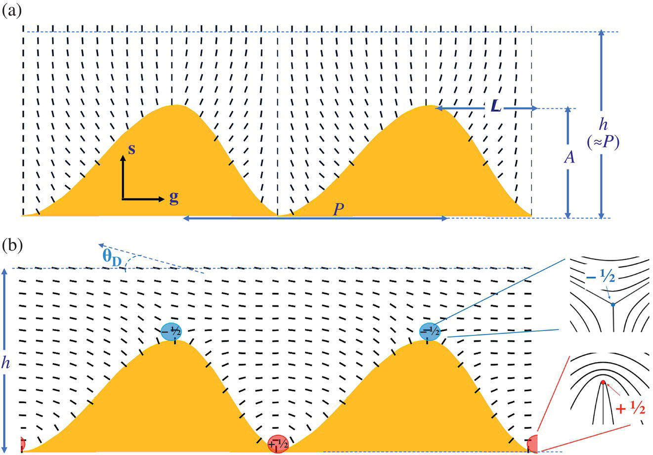
Figure 6.1 Zenithal bistable states of the nematic director close to a deep homeotropic surface relief grating of pitch P, amplitude A and blaze asymmetry L (if L < P/2). (a) The Continuous or C‐state, where the director has uniform vertical alignment (i.e. n || s) at the distance h from the lower surface. (b) The Defect or D‐state, wherein the director is again uniform at h from the lower surface but with a near‐planar alignment, with pretilt θD related to the degree of asymmetry L/P. Inset are sketches of the director profile around –½ and +½ topological defects in the director n field.
As a bistable surface, the grating can be used opposite a variety of surfaces to form the LCD, providing a number of different alignment geometries, each of which is bistable. The two most common geometries are shown in Figure 6.2. The first ZBD results were published using a switchable half‐wave plate [17], with the opposing surface being monostable (i.e. flat) homeotropic alignment, Figure 6.2a).
The bistable C‐ and D‐states correspond to vertically aligned nematic (VAN) and hybrid aligned nematic profiles. The VAN state should appear dark between crossed polarisers, whereas the HAN state transmits light when the grating, hence the D‐state director, is oriented at 45° to the polariser. Ignoring the director variation close to the grating surface and treating the director profile as linear (i.e. k11 = k33), the optimum cell gap is given by the half‐wave condition:

Figure 6.2 Example modes of a ZBD, based on choice of the opposing monostable surface. (a) Opposite a monostable homeotropic surface, the surface bistable C‐ and D‐states lead to vertically aligned nematic (VAN) and hybrid aligned nematic (HAN), respectively. (b) Opposite a monostable planar homogeneous surface with the preferred alignment direction r angled with respect to the grating vector g, gives the HAN in the C‐state, and a twisted nematic in the D‐state.
where the average tilt is taken as half way between the homeotropic condition and the D state (accurate if the splay and bend elastic constants are similar), with a birefringence related to the pretilt θD through:

Commercial devices use the bistable grating opposite a Planar Homogeneous [19], leading to a HAN configuration for the C‐state and a 90° TN for the D‐state. Here, the rubbing direction of the planar homogeneous surface r is arranged perpendicular to g, Figure 6.2b), and the nematic is weakly doped with chirality to ensure a single twist direction is maintained. For convenience, these homeotropic and planar homogeneous geometries are termed VAN and TN ZBD geometries, respectively.
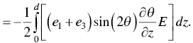
In addition to the bistable surface, a second difference between ZBD and conventional nematic LCD is the switching mechanism. Devices such as the TN respond to the root‐mean‐square of the applied voltage taken over a time sufficient for the director to reorient (e.g. the frame time). ZBD, on the other hand, responds to the electric field: it latches if an electrical pulse has sufficient magnitude, duration, and the correct polarity. Rather than coupling to the dielectric anisotropy, Δε, latching is realized using the flexoelectric polarization, the polarity associated with splay and bend deformations. That is, the free energy of Eq. (6.4) contains an additional term that is linear in the applied field given by:

Although the sum of splay e1 and bend e3 flexoelectric coefficients is small, around 100p Cm−1 for the strongly dipolar mesogens used for a ZBD [25], the elastic deformation and its associated electric polarity is concentrated close to the grating surface. This is further aided by the effect of a strongly positive Δε, which presses the elastic distortion still closer to the surface with applied field. Thus, typical latching times are around 1 ms for pulses of amplitude 2 V μm−1 [26]. Of course, the nematic liquid crystal used to form the cell will also switch due to the coupling between the dielectric anisotropy Δε and the applied RMS voltage, causing changes to the director orientation in the bulk of the device and a corresponding optical response.
The nematic continuum theory of Oseen, Frank, Ericksen, and Leslie [27] is a triumph of theoretical physics used by device scientists and engineers to understand and design ever more complex display devices. Perhaps, without such an accurate and useful theoretical basis, the modern LCD display industry would not have advanced to its current dominance. However, these theories usually treat the director as a simple unit vector, such as in the static‐free energy expression in Eq. (6.4). Such theories do not allow changes to the nematic order parameter S that high elastic strains may induce. Nematic defects are a good example of such strains: these are ≈50 nm regions where the director is undefined, and the order is effectively S = 0. Modeling of such systems then requires a Q‐tensor approach [28], where both orientation and order parameter magnitude may vary. This method has been applied to the ZBD device [29, 30], and most accurately with a direct comparison with experimental results in [31]. This work showed that the defects nucleated at the steepest parts of the grating and then moved across the surface toward the points of highest surface curvature under the influence of a positive electric field coupling to the positive flexoelectric coefficients. The defects’ trajectory could either follow the surface closely, as in [30–32], or separate from the surface into the bulk liquid crystal between the grating ridges, as shown in the example given in Figure 6.3. The path taken depends on the properties of the liquid crystal material, the grating surface, and the electrical pulses' timing [30]. Latching occurs at some point where the defects are sufficiently close to the regions of high surface curvature that the defects continue their path due to the influence of that curvature. A negative electrical pulse causes the defects to move toward each other until they annihilate on the surface. The negative defect is far more mobile than the positive [33], and hence the point of annihilation is close to the grating ridge.
![Schematic illustration of example of the electrical latching between the D- and C-states obtained using computational modeling of the Q-tensor [31].](https://imgdetail.ebookreading.net/2023/10/9781119745587/9781119745587__9781119745587__files__images__c06f003.jpg)
Figure 6.3 Example of the electrical latching between the D‐ and C‐states obtained using computational modeling of the Q‐tensor [31].
Figure 6.4 shows the optical response to a series of pulses for typical ZBD devices, wherein a positive pulse represents the electrical polarity applied to the grating electrode (a convention retained throughout this chapter). The transmission of ZBD in the VAN geometry ZBD to monopolar pulses that change sign after every two pulses is given in Figure 6.4a). The commercial liquid crystal E7 was used on a grating that produced a pretilt of θD = 20° so that the half‐wave‐plate condition calculated using Eqs. (6.5) and (6.6) gives dHAN = 2.7 μm. There is a momentary drop in transmission for each pulse due to the conventional RMS switching response of the positive Δε nematic material. However, positive pulses cause a change to the transmitting HAN state that does not decay after the pulse has been removed. The device has been latched from the non‐transmissive C‐state (VAN) to the transmissive D‐state (HAN in the optical half‐wave plate condition). This pulse sequence of alternating pairs of opposite polarity shows that the latching is strictly polarity dependent: a negative pulse applied to the device already in the C‐state causes a transient response, as the director close to the grating aligns parallel to the field, but the C‐state is retained due to the negative polarity. Only when a positive pulse of sufficient time and magnitude is applied does the device latches to the D‐state. Ensuring that the pulse duration and amplitude required to latch between either state is important for display optimisation. Early results for commercial STN mixtures produced typical latching with 40 V and 1 ms pulses [18]. However, low viscosity materials with higher dipole moments, and therefore flexoelectric polarisations, were developed [26], providing latching pulses of 16 V and 500 μs, such as those shown in Figure 6.4b).
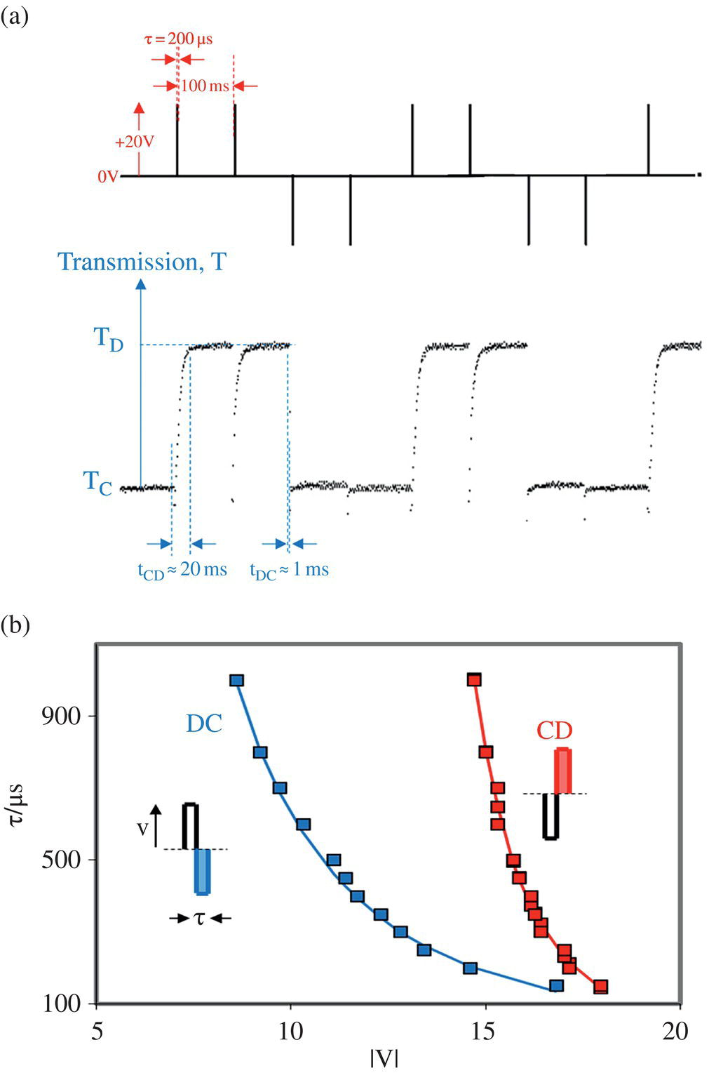
Figure 6.4 The electro‐optic response of typical Zenithal Bistable Devices. (a) Transmission T versus time response to a series of |20 V| 100 μs pulse pairs of opposite polarity for a 2.7 μm spaced ZBD with the commercial liquid crystal E7 in the VAN mode geometry [16]. (b) Latching response to bipolar pulses of Mixture B [26] measured in a 5.7 μm spaced ZBD in the TN geometry at 23 °C. Latching from D to C occurs when the trailing pulse is negative, and from C‐ to D‐state when the trailing pulse is positive.
In practice, the grating is designed with asymmetry and blaze, which is done for two reasons. Firstly, defects may be nucleated on the steep side of the surface either side of the grating ridge. Both pairs then interact with each other and prevent latching into the D‐state. With a blazed grating, the defect pair on the steeper side forms first and reaches the lines of highest surface curvature to latch before the second pair has moved far from its point of nucleation [31, 32]. The second reason for including blaze is to induce some pre‐tilt into the director of the D‐state. At h, the pretilt from the surface plane is approximately given by [34]:
For a symmetric sinusoidal grating L = P/2, the +½ and –½ defects are uniformly spaced and Eq. (6.8) shows that θD = 0°. In practice, a small amount of tilt is required for the domain‐free operation of the TN [8, 35], and a near‐sinusoidal grating is used. Note, it is important that the pretilt is not too high, since this will affect deleteriously the viewing angle associated with the D‐state, and gratings are usually designed to be nearly symmetric, with P = 0.80 μm and L ≈ 0.38 μm to give θD ≈ 6°.
Diagrams such as those of Figures 6.1 and 6.3 show the topological defects as points in a two‐dimensional space in a plane containing the director. However, the ±½ strength defects are lines running orthogonal to the plane of the director. The defects run along the grating groove ridges and troughs and meet and annihilate at two points to form a defect loop. Although held by the surface curvature by the grating, the defects must either run along the flat sides of the grating at the ends of the loop or into the bulk of the liquid crystal. One would expect the loops to be pinned at microscopic inhomogeneities in the cell that would occur on a practical grating surface. Without such pinning sites, the loops would only be stable if the deformation energies for the D‐ and C‐states are equal; otherwise, the loop would grow for a D‐state stable device (e.g. for deep gratings or high temperatures, where S is low, and defects are more stable) or shrink if the device is C‐state stable (shallow gratings or lower temperatures). Even if both states are of equal energy, disruption of the director profile through flow, such as that induced by pressing the front glass surface of the display, will cause the desired image to be erased. High levels of resistance to mechanical shock and a wide range of temperature operations are obtained in practiceby including regular π‐phase slips in the grating design [36], as shown in Figure 6.5. These provide concave and convex surfaces perpendicular to the grating, which stabilize the structures at regular intervals (usually spaced by several micron, as shown in Figure 6.5a). When considering the latching in 3D [37], the defects will nucleate and annihilate at the inflection points within each slip, and the defect moves along the surface of appropriate curvature, rather than as shown in the over‐simplified model of Figure 6.3. This type of defect motion is observed experimentally with high‐resolution polarized light microscopy.
6.3 Grating Fabrication and Supply Chain
Compared with other LCD alignment surfaces, either rubbed or photoaligned polymers, the ZBD surface requires considerable engineering to achieve consistent device operation. In a typical LCD manufacturing process, the time taken for each processing step is typically around 20–30 seconds. Photolithographic patterning of a sub‐micron grating directly onto LCD glass is not possible within this limit, so the mass production of ZBD LCD required the establishment of a high‐speed replication process. This is done by embossing a photopolymer using a structured film with the required shape.

Figure 6.5 Three‐dimensional structure of the ZBD grating. (a) Polarizing optical microscope image of a partially latched pixel. White lines are gratings in the D‐state and dark regions are C‐state. (b) Scanning Electron Microscope image of the ZBD grating structure showing the phase‐slips in the grating structure. (c) Principal of operation of the grating phase slip. Defect loops are stabilized by the concave and convex surface corners that result in the direction parallel to g, in addition to the concave and convex curvature of the groove bottoms and ridge tops.
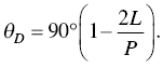
This replication process has several steps that are summarized in Figure 6.6. These are:
- Formation of photoresist master.
- Transfer of master pattern into nickel.
- Mass production of grating film from nickel.
- Formation of grating profile on LCD glass using grating film.
To make the photoresist master, a large area of glass substrate is thoroughly cleaned and coated with a perfect (pinhole‐free) photoresist layer. Chrome on glass mask with the required grating pattern pre‐etched is then placed in hard contact with this photoresist layer, and exposure is carried out using off‐axis UV radiation. This mask is typical of the type used in the photolithographic industry for deep UV patterning. It is typically 140 mm × 140 mm, suitable for producing small displays. However, for larger electronic paper applications, accurate steps and repeat are required to produce larger grating areas free from visible seams. After this exposure, the mask is moved by a precisely controlled distance across the photoresist before re‐establishing hard contact and carrying out a second exposure, Figure 6.7. This process is repeated until the target overall grating dimensions are exposed. Following subsequent thermal processing, the photoresist layer is developed to reveal a surface profile grating in which the seams between each exposure are invisible to the naked eye.
Figure 6.8 shows a typical grating profile. Off‐axis UV exposure generates a small amount of asymmetry in the grating groove profile (grooves tilt to the right), which is sufficient to control ZBD latching such that the C to D transition only leads to a single low tilt state. A typical seam is also shown.
After completing the mastering step, the following process involves transferring this profile into a nickel shim. This technology is well established in the CD/DVD mastering industry, which relies on creating nickel stampers to mass‐produce the disc media [38, 39]. This step ensures that a single master can be replicated into many km of film without damage.
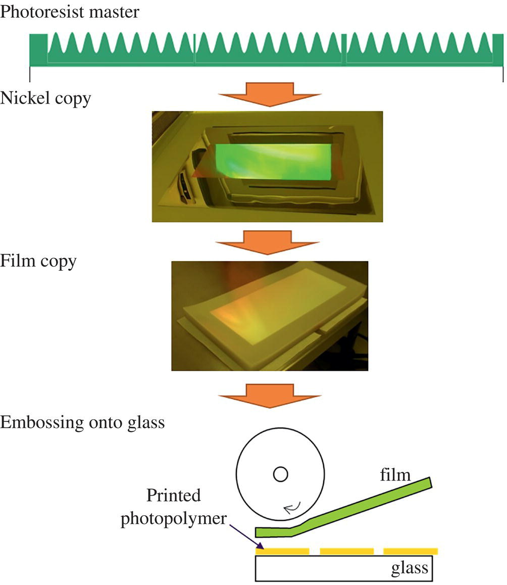
Figure 6.6 Multistep replication process that allows high speed mass production of ZBD LCDs.

Figure 6.7 Hard contact step and repeat exposures used to make the ZBD master grating.
Figure 6.8 (a) Scanning Electron Micrograph of a typical groove profile of ZBD master grating showing slight asymmetry. (b) Photograph of a typical 5 μm seam between two grating regions. The vertical slip lines can be seen in this optical image but not the horizontal grating grooves.

Figure 6.9 Schematic of process for transferring grating profile from nickel to film.
The photoresist master is first coated with a thin seed nickel layer via sputtering. This surface becomes one electrode in a large galvanic growing tank containing an optimum mix of electrolytes and other additives. Electrochemical deposition is done until the target nickel thickness is achieved, typically 150 to 450 μm. This 1st generation copy is then peeled from the glass substrate and is cleaned in a plasma chamber to remove photoresist material retained within the nickel copy's grooves. Thus, only one 1st generation copy can be made from each photoresist master. However, it is possible to then grow many 2nd generation copies from a single 1st generation nickel shim and many 3rd generation copies from each 2nd generation shim, and so on. In each case nickel‐nickel release is facilitated by the growth of a precisely controllable nickel oxide layer, which can be formed by wet processing before each galvanic growth process. This unique nickel property has made it the primary choice for multigenerational micropatterned tooling creation.
Direct embossing onto LCD glass using nickel is not well suited to the particular requirements of ZBD LCD. Therefore, another step is required in which the high‐cost nickel is converted into low‐cost plastic film. Figure 6.9 shows a schematic of this process. The nickel shim is mounted on a roller which is compressed against a second nip roller. A polymer film material (typically PET) is inserted between these rollers, and a UV‐sensitive photopolymer is poured into the gap between the PET film and the nickel shim. Roller rotation leads to casting the grating profile into a photopolymer layer formed between the nickel and the PET, which is then cured into a solid by high‐intensity UV. The photopolymer is designed to adhere firmly to the PET film while also readily releasing from the nickel surface. A protective release liner is added over the grating surface before wind‐up and subsequent sheeting. The resulting film is low cost, easy to transport, and can be stored for many years without performance degradation.
6.4 ZBD LCD Manufacturing Processes
The ZBD LCD is a passive matrix display technology, and much of the manufacturing process follows the same process steps as TN and STN displays. In fact, one substrate (the “P” plate) is processed with a rubbed polymer layer identically to TN/STN while the other “G” plate has some modified steps summarized in Figure 6.10. These steps are now described in more detail.
The basic process is to roller emboss the grating into a photopolymer layer by pressing the grating film into the uncured photopolymer and then hardening the grating through UV curing. The film is designed so that the grating area covers the glass so that the same film can be used regardless of the dimensions of the display being produced. Therefore, a first challenge is patterning the grating onto LCD glass so that the grating regions cover only the viewing area of each of the module locations on the mother‐glass. The grating must not cover the edge seal regions since seal materials are optimized for glass–glass bonding, and obviously, the grating should not cover bonding ledges since this would compromise the connection of driver ICs to row/column electrodes. Several methods have been proposed for controlling the grating extent [40], but the most successful in production has been selective adhesion. This method relies on controlling the relative adhesion energies at the interfaces between the relevant layers in the embossing process. A surfactant adhesion promoter is patterned onto the substrate using either ink‐jet or flexo‐printing to define the areas where the grating is retained on the mother‐glass. Figure 6.11 shows a schematic of these layers and the desired retention of the final LC alignment grating (ZBD photopolymer) after cure and peel. For the process to operate correctly, the relative adhesion between the photopolymer and glass EPS, film EPF and adhesion promoter EPA must each be considered, and the following relationship holds:

Figure 6.10 A simplified process flow for the manufacture of ZBD LCDs.
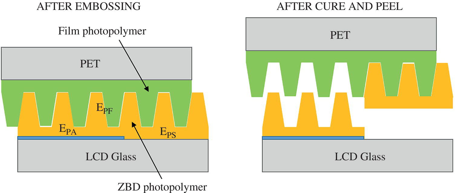
Figure 6.11 Definition of adhesion energies and subsequent layer retention after peeling. Subscripts denote uncoated substrate S, grating film F and adhesion promotor A.

Figure 6.12 Examples of typical active components to promote adhesion of ZBD photopolymer to SiOx (left) and ITO (right) regions of the substrate. Group R is compatible with photoactive groups in the ZBD photopolymer material.
EPS is naturally low (<1.0 J/m2) since the ZBD photopolymer has no intrinsic adhesion to the LCD substrate surface. The adhesion promoter contains two active components, Figure 6.12, in glycol solvents selected for optimum adhesion to both SiOx and ITO portions of the LCD glass surface. Such mixes are also effective on glass‐like hard coat layers, often applied over ITO electrodes in passive matrix LCDs. Once applied, the adhesion promotor solution is dried and cured at 130 °C to ensure full crosslinking of the silane material with itself as well as with the phosphate material.
The final challenge is to reduce the size of EPF. Since both the film photopolymer and the ZBD photopolymer use similar photoactive groups, the former is able to crosslink into the latter leading to an inseparable bilayer. However, it is possible to passivate the surface groups in the film photopolymer and reduce EPF to the range of 5–10 J/m2, which is well below EPA (typically >50.0 J/m2) [40].
The grating is formed on the mother‐glass employing a roller embossing process, as shown in Figure 6.13. Following the application and cure of the adhesion promotor, the LCD substrate is coated in a thin layer of ZBD photopolymer using inkjet printing. A proprietary photopolymer is used in production, which gives homeotropic alignment with the appropriate anchoring energy. Alternatively, a conventional photopolymer can be used and coated with a silane surfactant using a vapor deposition process [41]. Control of the anchoring energy then results by varying the surface density of the pendant groups. Following the photo‐polymer printing step, the mother‐glass is then laminated against film using a pair of rollers of optimum shore hardness that operate with an optimum applied pressure (P) and speed (V). Shortly after embossing, the photopolymer layer is cured via UV radiation, and the film is peeled to reveal a perfect copy of the grating structure on the LCD glass. If the embossing speed is too high or pressure too low, then the cured grating structure will include a significant “DC offset” of polymer below the modulation, and this leads to an undesirable voltage drop across the grating that is made worse by its relatively low electrical permittivity to the LC material [42]. With optimum range of conditions, the grating shown in Figure 6.14 is obtained.

Figure 6.13 Schematic of production embossing process.
The adhesion conditions of Eq. (6.9) ensure that unwanted photopolymer in areas outside the grating/display viewing areas is removed from the mother‐glass and remains attached to the film. Thus, the glass is spontaneously patterned in the peeling process. Once the grating has been formed, the substrate is ready to receive spacer beads and proceed through the remaining steps in the same fashion as a conventional LCD plate, Figure 6.10. Other than the adhesion promoter, grating film, and ZBD photopolymer, other display materials are common with those used for TN/STN displays. These include ITO glass, seal material, spacer beads, LC material, polarisers, and driver ICs.

Figure 6.14 SEM section showing an optimum ZBD grating. The pitch of the grating is 0.80 μm and the amplitude 1.05 μm.
6.5 Electrical Addressing
For any matrix display, the electric signals are applied from silicon driver ICs on the edges of the display. Conventional passive‐matrix addressed TN and STN LCD use the principles of RMS addressing to share signals across a matrix of row and column electrodes on the opposing display substrates to give the desired pattern of appropriate voltages when averaged over a frame time [7]. Usually, one of N rows has a strobe voltage +VS applied for an Nth fraction of the frame time, and this is synchronized with data voltage either +VD to not switch (due to the resultant VS − VD appearing across the pixel) or −VD to switch (due to the resultant VS + VD). For the remainder of the N‐1 rows of the frame, the row experiences the non‐discriminatory data for the other rows. Pixels in the switched state begin to decay toward the unswitched state unless refreshed in the next frame. This method means that discrimination results from only one Nth of each frame, thereby limiting the number of rows that can be addressed according to the steepness of the display's electro‐optic characteristic. For conventional LCD, overcoming this multiplexing limit relies on thin‐film‐transistors (TFT) located at each pixel to amplify the voltage signals received from the drivers. The thousands of rows can be addressed to form complex, high‐resolution images. Indeed, some candidates for electronic paper, such as electrophoretic displays, are not truly bi‐stable but are metastable. This means that they retain the image (and hence can operate with very low power) even after the signals are removed. However, a pixel will begin to latch into the opposing state with any small voltage, and hence a TFT is still required to isolate the pixel from the data voltages being applied to other rows of the panel.
The basics of driving a truly bi‐stable display, such as ZBD, are similar to conventional LCD RMS, except the strobe voltage VS is designed to lie close to the latching threshold. The data signal ±VD is applied synchronously with the polarity designed to give the appropriate resultant to the potential difference of row – column voltage. If VS + VD is sufficient, the pixels on that row will latch into the new state. Discrimination is achieved when VS – VD is not sufficient to cause that same change, and the pixels in the row do not latch. Thus, the image is formed line‐by‐line. The data voltage ±VD being applied to the other rows is far lower than the threshold and so, once latched, the row of pixels remains in their stored conditions, and the addressing signal can be applied to other rows without changing the latched state. Each addressing signal is arranged to give DC balance to prevent electrolytic damage to the liquid crystal, and avoid unwanted latching caused by long sequences of the same data signal.
Of course, the signal is applied to either change the state or leave it unchanged; a second signal is required to address each row for the other state that responds to the opposite polarity. There are several ways that this may be implemented [32]:
- Two‐field Addressing. A frame is divided into a positive field (selecting the D‐state) and a negative field (selecting the C‐state).

Figure 6.15 (a) Progressive line blanking (PLB) addressing scheme for ZBD. (b) Comparison of a typical ZBD latching characteristic for simple bipolar and PLB pulse sequences. PLP has a faster, lower voltage response since the blanking portion also couples to the positive Δε of the material, distorts the director profile closer to the grating and hence increases the flexoelectric polarization during the select portion.
- Blanking. The frame is divided into two fields, but the first field indiscriminately blanks the screen to one state (say black) so that the white pixels can be selected discriminately in the second field. The blanking is usually done line‐at‐a‐time, similarly to two‐field addressing, or a page /section blank may be used.
- Progressive Line Blanking. Rather than dividing the frame into two fields, each line is addressed in sequence with a blanking portion, followed by a selection portion. An example of such a scheme used for ZBD is shown in Figure 6.15.
- Line‐ahead blanking. The blanking pulse can have sufficient electrical impulse to blank into one state (usually C) regardless of the applied data. Thus, a row can be blanked during the addressing signal for the previous row or rows. Although potentially faster, this type of scheme isn't usually done using conventional STN type drivers since they are restricted to four voltage levels only.
- Strobe‐extension. As with Line‐ahead blanking, the selection strobe may be extended into the following lines to help improve response time further. Again, this is not used with STN drivers due to the four‐level restriction.
For many simple applications, such as shelf‐edge label displays, the slow speed of the basic addressing schemes such as Two‐field or Line‐at‐a‐time Blanking is adequate and readily applied using standard STN drivers. Where addressing speed is important, faster schemes such as line‐ahead blanking allow line addressing times significantly faster than 1 ms per line to be achieved.
6.6 Optical Configurations
Although it is possible to create a scattering mode ZBD LCD [43], this technology is usually configured to operate by modulating polarized light [44]. Before considering the bulk optical properties of the LCD alignment states, it is important to realize that the grating itself has a strong optical effect due to both diffraction and form birefringence. In a practical LCD, the design is chosen to minimize these effects since they inevitably add coloration to the white state and/or reduce the contrast ratio. This is achieved by ensuring that the bistable grating surface is adjacent to the front polariser in the LCD cell (Figure 6.16) and further that the polarizer is aligned so that its transmission axis is perpendicular to the LC slow axis (so‐called “o‐mode”). Since the LC remains in the plane of the page for both bistable configurations, the incident light only samples no of the LC material. By engineering the ZBD photopolymer such that its refractive index (ng) is equal to no, it is thus possible to make the grating‐LC interface optically invisible. With the grating effects removed, it is possible to readily model the optical viewing of the ZBD LCD.

Figure 6.16 Two possible arrangements (e‐mode or o‐mode) of the front polariser with respect to the LC and grating.
Regarding Figure 6.16, the front (transmissive) and rear (reflective) polarisers are typically placed in the crossed configuration such that the TN state is white and the HAN state is black. The viewing properties of these two states are shown in Figure 6.17. For this example, the bistable grating tilt angles are 5° and 90°, the rubbed polymer tilt is 5°, Δn = 0.12, and the cell gap is set to the first Gooch and Tarry minimum [22] given by Eq. (6.3). The wide viewing of the bright TN state is perhaps surprising since TN LCD is generally regarded as a narrow viewing angle mode. However, it should be recognized that multiplexed TN usually operates between two non‐zero voltages leading to higher LC director tilt in the mid‐cell region, which significantly compromises viewing. In contrast, the configurations in Figure 6.17 are both maintained at zero applied voltage, and so the TN state supports a low director tilt (averaging about 3°) throughout the bulk of the device.
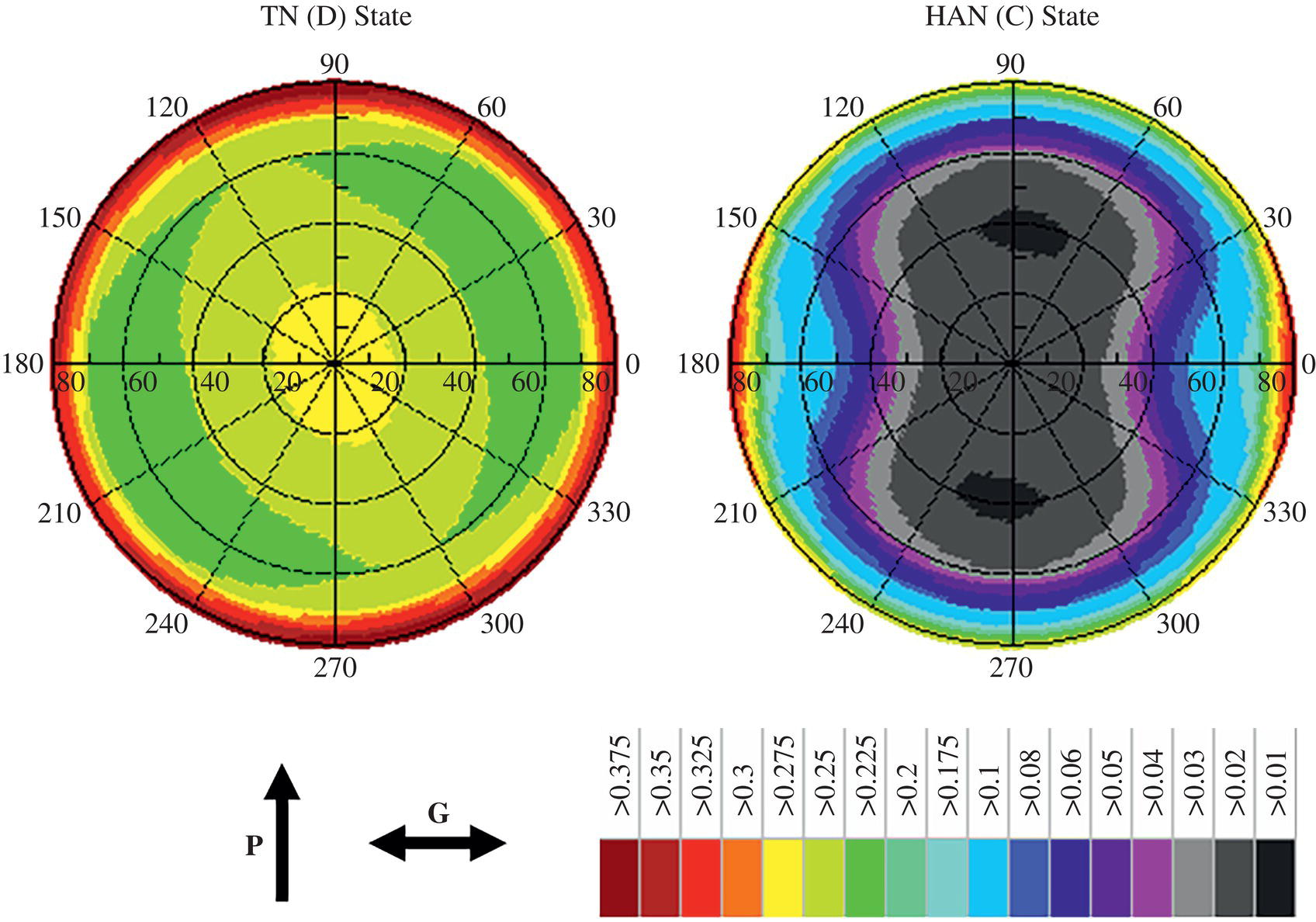
Figure 6.17 Modeled reflectivity of the bright (TN) state and the dark (HAN) state as a function of viewing direction. The orientation of P plate rubbing direction and G plate alignment is also shown. The model assumes specular reflection.
The dark HAN state, has the significant tilt in the mid‐cell region, which leads to narrowing the viewing properties in the horizontal plane. Thus, the display's contrast ratio is worse in one orientation compared to the other. Usually, this direction can be chosen to best match the intended use of the display. It is also possible to increase this viewing with compensation layers if required. One other advantage of using the TN (D) state as the white state of the display is that this is the configuration that the ZBD LCD cools into after LC filling and annealing (to a temperature above the liquid crystal to isotropic transition, TNI). Therefore, the unlatched interpixel gaps across the active area of the display will remain white, thus adding to the overall reflectivity of the display.
As well as viewing properties, it is important to consider the optimization of white state color balance and viewing properties. For a given LC and polarisers, it is possible to adjust the color hue of the display by changing the optical retardation, Δnd. In particular, to raise it to a level in‐between the 1st and 2nd Gooch‐Tarry minimum values of Eq. (6.2). Figure 6.18 shows the modeled and measured color coordinates (CIE1931) for the TN state in response to changes in the LCD cell gap (Δn = 0.12). The modeled color passes very close to the D65 white point for an adequate LC layer thickness of 6.3 μm.
Figure 6.17 shows the reflective efficiency of the ZBD mode (assuming specular reflection). However, in practice, there must be consideration of how incident light is reflected. In particular, the level and form of light diffusion are key to avoiding the “metallic” specular appearance observed in some reflective display modes. Conventional diffusers are included in the reflective polarizer materials and typically consist of high index beads in a low index polymer matrix. These provide a Gaussian scattering profile (Figure 6.19) that leads to high reflectivity only in the vicinity of the specular reflection angle; this is undesirable for wide viewing. However, recently many reflective LCDs have utilized structural diffusers [45], which produce a “flat‐top” diffusion profile that can also be asymmetric around the specular angle to take advantage of particular display illumination conditions.
The effect of structural diffusers is demonstrated in Figure 6.20, which displays both diffuser types. These were photographed with a fixed camera and lighting conditions with the displays at four different tilt angles. The structural diffuser enables much higher reflective intensity, especially at angles well away from the specular condition. Indeed, the introduction of structural diffusers can be considered one of the leading performance breakthroughs for reflective LCDs (including ZBD) in the last 10 years. They allow LCDs to exhibit reflective properties closer to a Lambertian reflector and thus provide a more “paper‐like” appearance to the display.
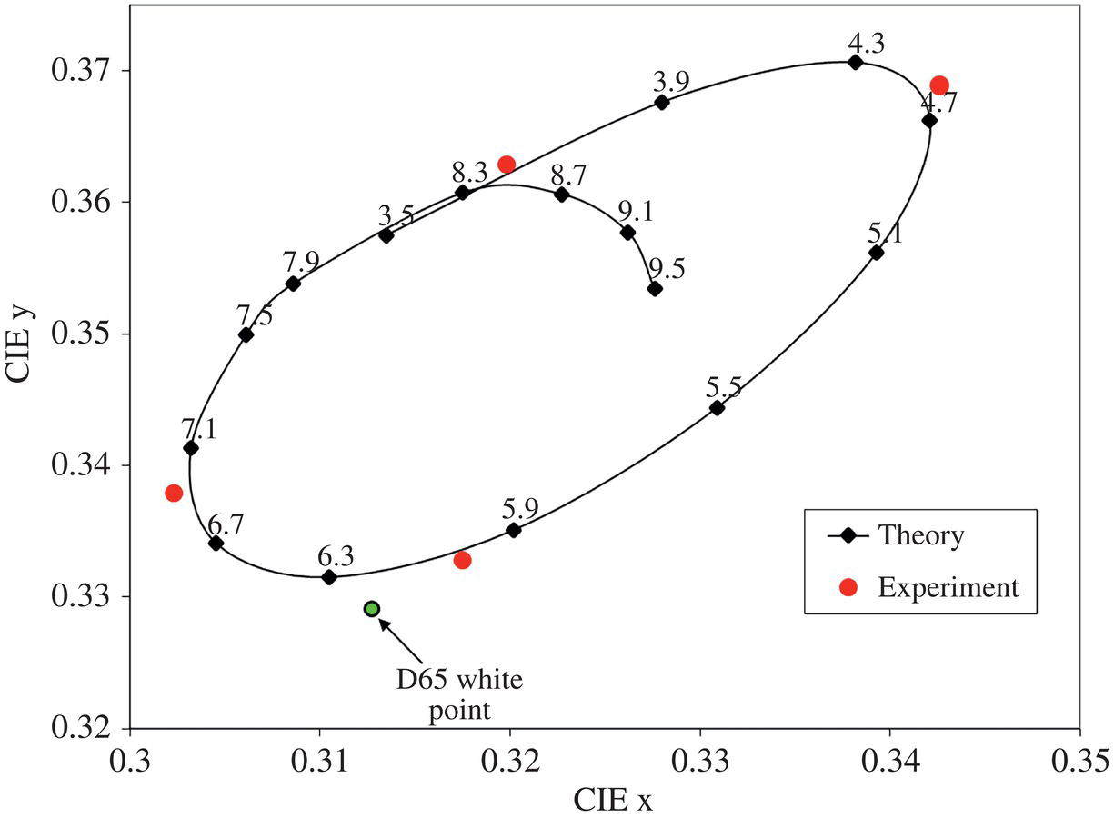
Figure 6.18 Modeled and measured color coordinates of the ZBD LCD white state as a function of cell gap (labels shows gap in microns).
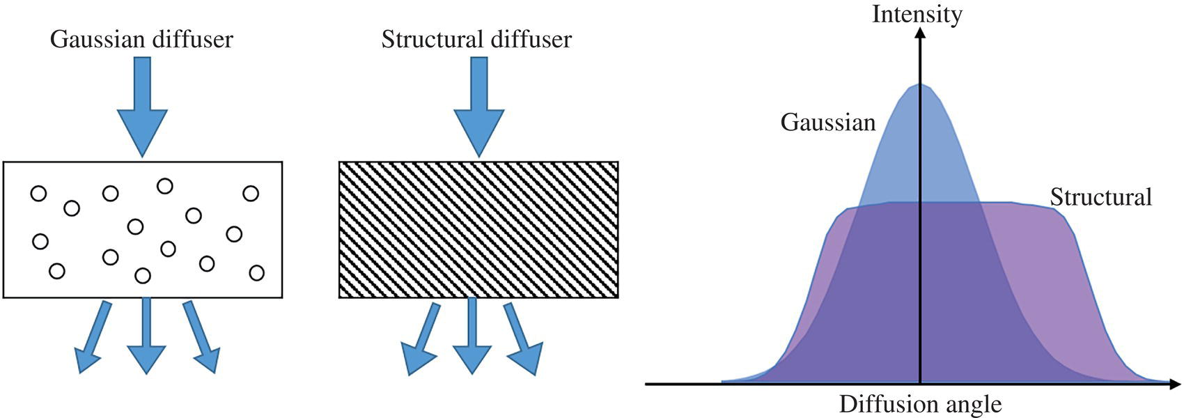
Figure 6.19 Scattering from conventional (Gaussian) diffusers and structural diffusers. The latter provide a “flat‐top” diffusion profile which can also be asymmetric with respect to the incident light direction.
Figure 6.20 Reflectivity of two ZBD LCDs employing conventional (left) and structural (right) diffuser layers on top of the rear reflective polariser. Viewing conditions are varied from specular (top left photo) to around 45° from specular (bottom right photo).
6.7 Novel Arrangements
As well as a two‐polariser fully reflective LCD mode, the ZBD technology can be deployed in other configurations, which can have merits for particular applications. A useful example of this is the dual‐layer display, the configuration for which is shown in Figure 6.21. This display mode [46] combines a low power/zero power reflective display on top of a full color emissive OLED display (or a transmissive LCD). This allows a‐mode display with a low‐power black/white mode or a higher power color video mode. Usually, the OLED display incorporates a wide‐band quarter‐wave plate at the front as an anti‐reflection coating. The polariser/waveplate pair is required to suppress the very high reflectivity from the metal tracks on the OLED backplane. The idea [46] is to replace the static quarter‐wave plate with a bistable retarder to allow the display to operate in an electronic‐paper mode with the OLED switched off. ZBD is well suited to such a configuration since it can be tuned to act as a bistable waveplate and a has a very high aperture ratio (passive matrix). A HAN/VAN ZBD mode is then inserted between the optical layers and the OLED backplane. In the VAN state, the ZBD layer does not disturb the antireflection properties of the polariser/waveplate layer, thus maintaining a low reflectivity. However, a suitably optimized HAN state can cancel out the fixed waveplate and lead to a bright reflectivity that can be suitably diffused by the insertion of an appropriate structural diffuser. Figure 6.21 shows the operation of such a prototype that can will enable a display product that can display a zero‐power fixed image while also allowing full color multimedia operation when required.

Figure 6.21 Configuration of ZBD/OLED dual layer display and resulting reflective and emissive performance.
A different dual‐mode device can be considered in which a bistable mode such as ZBD is combined with a TFT backplane [47]. A typical configuration is shown in Figure 6.22, in which a HAN/VAN mode ZBD is constructed onto a TFT backplane that carries transflective electrodes. Operation of the TFT at high (≈ 15 V) voltage allows the ZBD surface to be latched into the HAN (white) or VAN (black) states. In addition, video‐rate greyscale operation is available by first latching the whole display into the white state and then using standard low voltage TFT addressing to modulate the HAN state brightness. A typical prototype is shown in Figure 6.22, and a close‐up of the pixels latched into both the bistable states. Suitable diffuser and color filter layers should also be added to operate fully. This mode can also be considered using a fully reflective electrode and a frontlight.
Both modes shown in this section have practical limitations which are yet to be overcome. Firstly, both use single‐polariser modes in which the polarizer is at 45° to the grating grooves. This leads to diffraction and form birefringence effects. While the latter can be compensated with optical films, the latter be reduced by reducing the grating periodicity to sub‐optical values. This requires utilization of emerging grating mastering techniques. Secondly, to achieve practical cell gaps (3–4 μm or greater), single polariser modes should use LC materials with low Δn (0.08–0.10). Such materials are challenging to utilize in a ZBD mode while maintaining a usefully wide operating temperature range.
Figure 6.22 Dual mode display in which a ZBD LCD is fabricated on an active‐matrix backplane to allow a fixed image mode or a video mode. A working prototype is shown along with a close‐up view of pixels in two bistable states.
6.8 Conclusions
One of the most important paper features, which all electronic ‐paper must aspire to, is its ultra‐low‐cost. Among the lowest cost displays available are simple reflective TN LCD. They are passive matrices and do not require TFTs to drive them. This low cost is delivered because the liquid crystal materials, glass, alignment layers, polarisers, and electronic drivers are commoditized components. The ZBD is a bistable equivalent to the TN option, with only the additional step of the grating fabrication required. The large‐scale replication of the ZBD grating described here provides a means of maintaining that low cost while offering unlimited image complexity through its line‐at‐a‐time passive matrix addressing. Of course, electronic paper must also offer high reflectivity across a wide range of viewing angles. The contrast of ZBD is world‐beating for a bistable technology. Near the specular angle, the light reflected is also high and typically higher than a Lambertian reflector. However, many electronic paper applications require a wide range of viewing angles, for which the properties of the paper‐like Lambertian reflector are advantageous. For such applications, improved viewing has been achieved using additional optical films, albeit at some small additional cost to the panel. Table 6.1 summarizes the current state of commercially available ZBD devices.
Table 6.1 Operating parameters of a typical commercial ZBD display.
| Parameter | Value |
|---|---|
| Temperature range | −10 to +70 °C |
| Operating voltage (typical) | 20 V (20 °C), 40 V (−10 °C) |
| Optical response time | ton = 20 ms, toff = 0.1 ms (5.0 μm cell gap) |
| Cell gap | 4.0–8.0 μm (2 polariser mode) |
| Reflectivity | 34% (fully diffuse illumination) |
| Display update speed | 4.0 ms per line (@20 °C). |
| Display complexity limit | Infinite number of lines possible. |
| Bistable image lifetime | >10 years (between −40 and +85 °C) |
Acknowledgments
JCJ wishes to thank RCUK (EPSRC) for an Advanced Manufacturing Fellowship (EP/S029214/1).
References
- 1 Heikenfeld, J., Drzaic, P., Yeo, J.‐S., and Koch, T. (2011). A critical review of the present and future prospects for electronic paper. J. Soc. Inf. Disp. 19 (2): 129–156.
- 2 Comiskey, B., Albert, J.D., Yoshizawa, H., and Jacobson, J. (1998). An electrophoretic ink for all‐printed reflective electronic displays. Nature 394: 253–255.
- 3 Hattori, R., Yamada, S., Masuda, Y., and Hihei, N. (2003). Novel type of bistable reflective display using quick response liquid powder. Proc. SID Int. Symp. Dig. Tech. Pap. 34 (1): 846–849.
- 4 Heikenfeld, J., Zhou, K., Kreit, E. et al. (2009). Electrofluidic displays using Young–Laplace transposition of brilliant pigment dispersions. Nat. Photonics 3: 292–296.
- 5 Hayes, R.A. and Feenstra, B.J. (2003). Video‐speed electronic paper based on electrowetting. Nature 425: 383–385.
- 6 Back, U., Corr, D., Lupo, D. et al. (2002). Nanomaterials‐based electrochromics for paper‐quality display. Adv. Mater. 14 (11): 845–848.
- 7 Jones, J.C. (2017). Liquid crystal displays. In: The Handbook of Optoelectronics. Second Edition. Volume 2: Enabling Technologies. Chapter 6 (ed. J.P. Dakin and R.G.W. Brown), 137–224. Boca Raton, FL: CRC Press.
- 8 Jones, J.C. (2018). Fifty years of the liquid crystal display. Liq. Cryst. Today 27 (3): 44–70.
- 9 Jones, J.C. (2012). Bistable LCDs. In: Handbook of Visual Display Technology (ed. J.C. Janglin, W. Cranton and M. Fihn), 1507–1543. Berlin Heidelberg: Springer Verlag.
- 10 Greubel, W. (1974). Bistability behavior of texture in cholesteric liquid crystals in an electric field. Appl. Phys. Lett. 25 (1): 5–7.
- 11 Coates, D., Crossland, W.A., Morrissy, J.H., and Needham, B. (1978). Electrically induced scattering textures in smectic A phases and their electrical reversal. J. Phys. D. Appl. Phys. 11: 2025–2034.
- 12 Clark, N.A. and Lagerwall, S.T. (1980). Submicrosecond bistable electrooptic switching in liquid crystals. Appl. Phys. Lett. 36: 899–901.
- 13 Berreman, D.W. and Heffner, W.R. (1981). New bistable liquid crystal twist cell. J. Appl. Phys. 52 (4): 3032–3039.
- 14 Dozov, I., Nobili, M., and Durand, G. (1997). Fast bistable nematic display using monostable surface switching. Appl. Phys. Lett. 70 (9): 1179–1181.
- 15 Thurston, R.N., Cheng, J., and Boyd, G.D. (1980). Mechanically bistable liquid‐crystal display structures. IEEE Trans. Electron Dev. ED‐27 (11): 2069–2080.
- 16 Bryan‐Brown, G.P., Brown, C.V., and Jones, J.C. (2001). US Patent 6,456,348. Priority date 16th October 1995.
- 17 Bryan‐Brown, G.P., Brown, C.V., Jones, J.C. et al. (1997). Grating aligned bistable nematic device. Proc. SID Int. Symp. Dig. Tech. Pap. 28: 37–40.
- 18 Jones, J.C., Bryan‐Brown, G.P., Wood, E.L. et al. (2000). Novel bistable liquid crystal displays based on grating alignment. Proc. SPIE 3955, Liq. Cryst. Mater. Dev. Flat Panel Displays 3955: 84–93.
- 19 Wood, E.L., Brett, P.J., Bryan‐Brown, G.P. et al. (2002). Large area, high resolution portable ZBD display. Proc. SID Int. Symp. Dig. Tech. Pap. 33 (1): 22–25.
- 20 Jones, J.C. (2008). The zenithal bistable display: from concept to consumer. J. Soc. Inf. Disp. 16 (1): 143–154.
- 21 Jones, J.C. (2017). Defects, flexoelectricity and RF communications: the ZBD story. Liq. Cryst. 44 (12): 2133–2160.
- 22 Gooch, C.H. and Tarry, H.A. (1975). The optical properties of twisted liquid crystal structures with twist angles less than or equal to 90 degrees. Appl. Phys. 8: 1575–1584.
- 23 Berreman, D.W. (1971). Solid surface shape and the alignment of an adjacent nematic liquid crystal. Phys. Rev. Lett. 28 (26): 1683–1685.
- 24 Kitson, S. and Geisow, A. (2002). Controllable alignment of nematic liquid crystals around microscopic posts: stabilization of multiple states. Appl. Phys. Lett. 80 (19): 3635–3637.
- 25 Kischka, C., Elston, S.J., and Raynes, E.P. (2008). Measurement of the sum (e1+e3) of the flexoelectric coefficients e1 and e3 of nematic liquid crystals using a hybrid aligned nematic (HAN) cell. Mol. Cryst. Liq. Cryst. 494: 93–100.
- 26 Jones, J.C., Beldon, S., Brett, P. et al. (2003). Low voltage zenithal bistable devices with wide operating windows. Proc. SID Int. Symp. Dig. Tech. Pap. 34: 954–957.
- 27 Stewart, I.W. (2004). The Static and Dynamic Continuum Theory of Liquid Crystals. CRC Press.
- 28 de Gennes, P.G. and Prost, J. (1993). The Physics of Liquid Crystals. Oxford: Clarendon Press.
- 29 Parry‐Jones, L.A. and Elston, S. (2005). Flexoelectric switching in a zenithally bistable nematic device. J. Appl. Phys. 97: 093515.
- 30 Spencer, T.J. and Care, C. (2006). Lattice Boltzmann scheme for modeling liquid‐crystal dynamics: zenithal bistable device in the presence of defect motion. Phys. Rev. E 74 (061708): 1–14.
- 31 Spencer, T.J., Care, C., Amos, R.M., and Jones, J.C. (2010). A zenithal bistable device: comparison of modelling and experiment. Phys. Rev. E 82 (021702): 1–13.
- 32 Jones, J.C. (2014). Bistable nematic liquid crystals. In: The Handbook of Liquid Crystals. 2nd Edition. Volume 8, Chapter 4 (ed. J.W. Goodby, P.J. Collins, T. Kato, et al.), 87–145. New York: Wiley.
- 33 Tang, X. and Selinger, J.V. (2019). Theory of defect motion in 2D passive and active nematic liquid crystals. Soft Matter 15: 587.
- 34 Wood, E.L., Hui, V.C., Bryan‐Brown, G.P., et al. (2006) US patent 7,053,975; priority date 20th July 2000.
- 35 Raynes, E.P. (1974). Improved contrast uniformity in twisted nematic liquid‐crystal electro‐optic display devices. Electron. Lett. 10 (9): 141–142.
- 36 Jones, J.C. (2011). US patent 8,199,295; priority date 2nd July 2003.
- 37 Day, S.E., Willman, E., James, R., and Fernandez, A. (2008). Defect loops in the zenithal bistable display. Proc. SID Int. Symp. Dig. Tech. Pap. 39 (1): 1034–1037.
- 38 Orlic, S. (2017). Optical information storage and recovery. In: The Handbook of Optoelectronics. Second Edition. Volume 2: Enabling Technologies. Chapter 13 (ed. J.P. Dakin and R.G.W. Brown), 505–540. Boca Raton, FL: CRC Press.
- 39 https://en.wikipedia.org/wiki/Compact_Disc_manufacturing.
- 40 Bryan‐Brown, G.P., Walker, D.R.E., and Jones, J.C. (2009). Controlled grating replication for the ZBD technology. Proc. SID Int. Symp. Dig. Techn. Pap. 40: 1334–1337.
- 41 Jones, S.A., Bailey, J., Walker, D.R.E. et al. (2018). Method for tuneable homeotropic anchoring at microstructures in liquid crystal devices. Langmuir 34 (37): 10865–10873.
- 42 Amos, R.M., Bryan‐Brown, G.P., Wood, E.L., et al. (2010). US patent 7,824,516, priority date 13th July 2003.
- 43 Jones, J.C. (2013). US patent 8,384,872, priority date 30th Nov 1999.
- 44 Jones, J.C. and Bryan‐Brown (2010). Low cost zenithal bistable device with improved white state. Proc. SID Int. Symp. Dig. Tech. Pap. 41: 207–211.
- 45 Ishinabe, T., Kusama, K., Fujikake, H., and Shoshi, S. (2013). Wide‐color‐gamut and wide‐viewing‐angle color reflective LCD with novel anisotropic diffusion layer. Proc. SID Int. Symp. Dig. Tech. Pap. 44: 350–353.
- 46 Bergquist, J. (2011). Patent application WO/2011/107826, priority date 1st March 2010.
- 47 Jones, J.C. (2006). US patent 7,019,795, priority date 20th June 2002.