7
Reflective LCD with Memory in Pixel Structure
Yoko Fukunaga
Senior Engineer, Panel Design Department, Japan Display Inc.
7.1 Introduction
Low‐temperature polycrystalline silicon (LTPS) is a well‐established backplane thin film transistor (TFT) technology used for flat panel displays. LTPS TFT technology allows us to integrate complementary MOS (CMOS) circuits onto the glass. Development of the system‐on‐glass (SOG) display using LTPS TFT liquid crystal displays (s) has been hot technology topics in the late 1990s and early 2000s. SOG technology allows us to integrate various functional circuits onto display panels, such as timing controllers, display drivers, and decoders.
Memory in pixel (MIP) LCD is one of the unique applications of SOG technologies. It is one of the best ways to reduce LCD driving power because this approach needs no image data refreshment when displaying still images [1–7].
Reflective LCD technology is also one of the best ways to reduce display power consumption. The backlight consumes a large amount of transmissive LCD's power. A reflective LCD utilizes environmental light and has no need to turn on an auxiliary light when the environment is bright enough.
MIP technology and reflective LCD technology are good combinations because MIP circuits can be integrated behind the reflective pixel electrode without sacrificing the reflective aperture ratio.
LTPS SOG technology makes it possible to integrate display interface circuits onto a glass border area. An MIP LCD with display interface circuits is a good example of a fully integrated digital display system. It works as a digital memory device that can display memory data on the screen. A fully digital interface display requires fewer control and data signals to drive it. This reduces the number of flexible‐on‐glass (FOG) pads required, and allows the system to be driven directly by a microcontroller. In other words, it does not require an external display driver IC, which consumes large amounts of power for display operations. Reflective displays are suitable for maximizing outdoor visibility with low power consumption. MIP reflective LCD technology is advantageous for products that require a small FOG pad design and super low power operation. Therefore, they have been widely used for sports watches over the last decade.
This chapter traces the development of MIP reflective display technologies and their applications. It includes a review of the basic technology behind an MIP circuit and its pixel design and LCD optical design and the design characteristics of available market products and their super low power operations. The chapter also reviews selected applications of MIP reflective LCDs and previews future possibilities for this technology and its applications.
The following section provides an overview of the MIP technology, how it works, and how to drive it.
7.2 Memory in Pixel Technology and Its Super Low Power Operation
MIP technology is one of the best ways to reduce LCD driving power because this approach needs no image data refreshment when displaying still images [1–7].
Figure 7.1 shows the pixel design concept of a MIP reflective LCD. A static random‐access memory (SRAM) circuit is embedded behind the reflective electrode in each sub‐pixel.
Figure 7.2 compares a conventional active‐matrix LCD with a MIP LCD.
Figure 7.2a shows a system block diagram and an equivalent pixel circuit of a conventional active‐matrix LCD. Each pixel datum is written through the signal line when the gate line is on. The pixel datum is stored as a charge of the capacitor between the pixel electrode and the common electrode (COM). When the gate is off (voltage holding period), the pixel voltage decays depending on the leak current of the pixel TFT and the voltage holding ratio of the liquid crystal (LC) cell with the storage capacitor in parallel. The pixel data need to be refreshed at an appropriate cycle, such as 60 Hz, to avoid flickering issues caused by voltage decay. The Horizontal Driver (H‐Driver) and the Vertical‐Driver (V‐Driver) have to continuously refresh all the pixel data.
Figure 7.2b shows a system block diagram and an equivalent pixel circuit of a MIP LCD, while Figure 7.3 shows an equivalent MIP circuit with applied signals to drive the LC.
The SRAM memory datum of each sub‐pixel is written through the signal line when the gate is on. Each sub‐pixel datum is stored in the SRAM. The OUT or the XOUT switch is selected according to the memory datum. As a result, the pixel electrode is connected to a line that conveys an FRP or an XFRP signal. An FRP signal is equivalent to a signal that drives a common electrode (VCOM signal), while an XFRP signal is the inverse of a VCOM signal. In a normally‐black mode LCD, when an FRP signal is selected, there is no voltage applied to a LC pixel, which results in a black image being shown. Conversely, the selection of an XFRP signal results in a white image being shown. The voltage polarity applied to LC is toggled at an appropriate cycle by changing the VCOM/FRP and XFRP signal polarity to avoid flickering and image sticking issues caused by the offset voltage of the LC capacitor.
As shown in Figure 7.2, all the display image data are stored in SRAMs placed in the active display area (A.A.). There is no need to operate the H‐Driver and the V‐Driver when displaying a still image.
Generally, power consumption (P) is estimated by
Figure 7.1 Design concept of memory in pixel (MIP) reflective LCD.
Figure 7.2 System block diagram and equivalent pixel circuit of a conventional active‐matrix LCD and a memory in pixel LCD.
Figure 7.3 Equivalent MIP circuit with applied signals to drive a liquid crystal.
The majority of power in a conventional active‐matrix LCD is consumed to drive signal lines. The charging and discharging current to signal lines, which act as a large capacitor, is required at a high‐frequency level.
On the other hand, when displaying a still image, a MIP LCD consumes only a small amount of charging and discharging current to the LC capacitor at a low enough frequency to avoid flickering and image sticking. This results in an ultra‐low‐power operation.
The main difference between a MIP reflective LCD and other low power memory display modes, such as an electrophoretic display and a cholesteric LCD, is that the display mode itself does not have memory characteristics. Generally, memory display modes have larger capacitance per unit area. They consume larger amounts of power to refresh an image, and they cannot show moving images.
A MIP LCD utilizes an SRAM circuit as digital memory, and an LC on the memory operates as a digital optical shutter. The combination of the separated functions allows the system to achieve super‐low power operation to display moving images.
Even when displaying moving images, a MIP LCD consumes lower power than a conventional LCD. The following section describes the reason why.
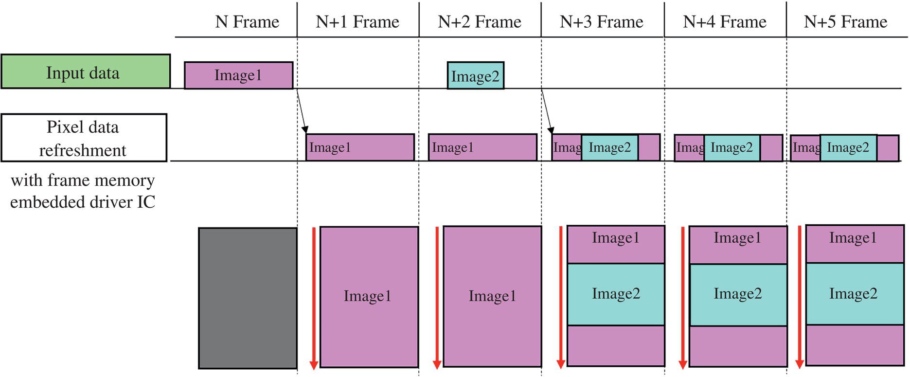
Figure 7.4 Display image data transfer of a conventional active‐matrix LCD.
Figure 7.4 illustrates how a conventional active‐matrix LCD transfers input image data display via a display driver IC with frame memory. For example, full‐screen image data (“Image 1”) are sent to the display driver IC, and the data (“Image 1”) are stored in the frame memory. The frame data (“Image1”) are converted to analog signals and transferred to all the pixels via the signal lines in the next frame period. When some portion of the image data (“Image2”) needs to be changed, only the data, “Image 2,” are sent to the display driver IC, and the portion is overwritten on the “Image 1” data. The driver IC autonomously refreshes the full‐screen data at a frame rate using the data stored in the frame memory.
Figure 7.5 illustrates how a MIP LCD transfers input image data to a display area. Full‐screen image data (“Image 1”) are sent to the active area through the display interface circuits embedded on the border area. The data are directly stored in the SRAMs behind the pixel electrodes. When some portion of the image data (“Image2”) needs to be changed, the gate lines corresponding to the area (“Image 2”) are selected and overwritten. The power consumption to overwrite the display is proportional to the gate lines to be written. This operation reduces power consumption when images need to be partially updated.
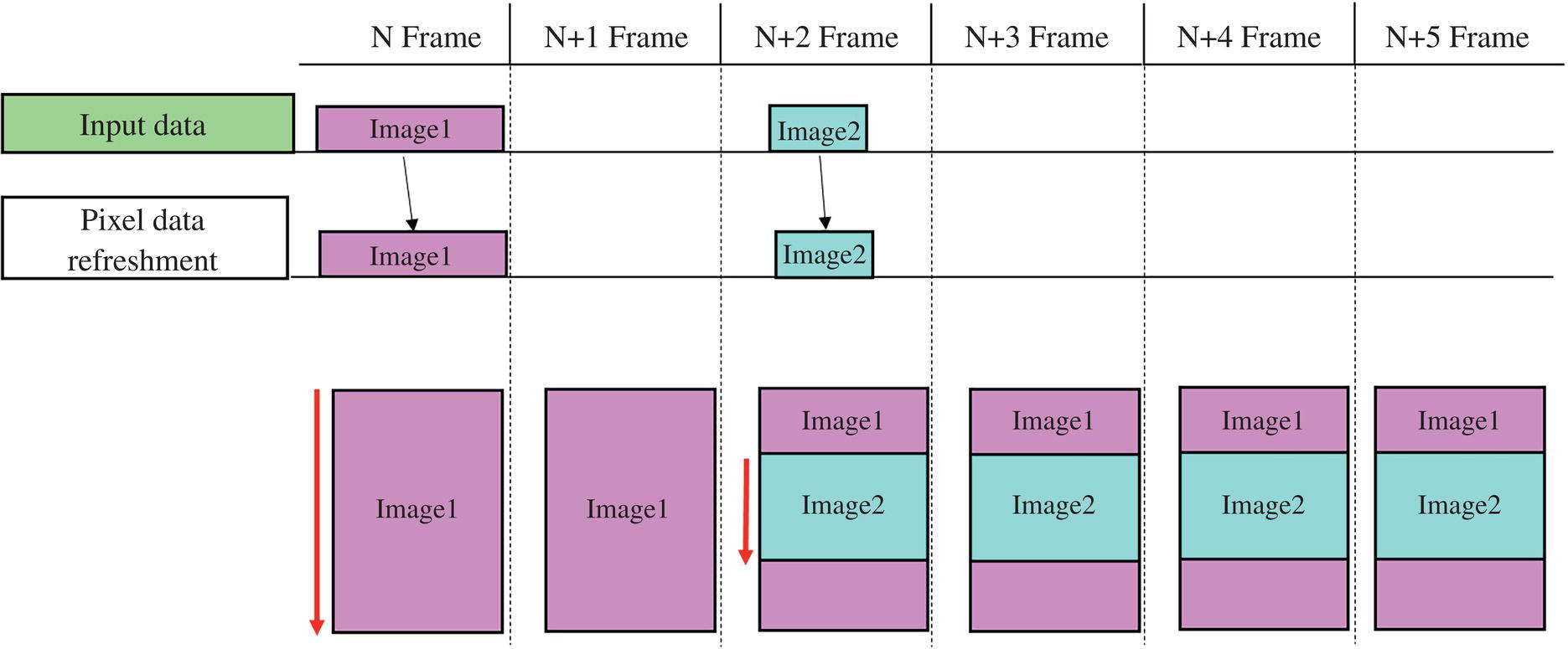
Figure 7.5 Display image data transfer of an MIP LCD.
With a conventional active‐matrix LCD, the gradation of each subpixel is controlled by analog voltage. The driver IC needs to equip digital/analog converters and analog amplifiers to drive the signal lines, continuously consuming bias current.
In contrast, a MIP LCD is a fully digital display. It is driven by digital signals.
To return to the equation to estimate power consumption (P),
A MIP LCD system can eliminate static current to generate analog signals and reduce the frequency to drive signal lines (f), and reduce the display area (C) to be rewritten. This contributes to super‐low levels of power operation.
However, because of this full digital display feature, each subpixel of MIP LCD cannot express grayscale. The following section addresses the challenge of showing grayscale using MIP LCDs.
7.3 Sub‐Pixel Pattern to Show Gray Scale
A MIP full digital LCD design is advantageous to realize super‐low power operation, but expressing grayscale is a major challenge. The so‐called “area coverage modulation” method expresses grayscale by combining dots, as has been the case with printing devices. However, increasing pixel bits and resolution is disadvantageous, and there is a risk of pattern noise.
To apply this method to a MIP reflective LCD, each pixel has to be divided into the number of grayscale bits, and the bit number of SRAM has to be laid out within the pixel area. As shown in Figures 7.2 and 7.3, MIP circuits are more complicated than conventional active‐matrix pixel circuits. For the reasons described above, MIP LCDs have severe limitations when trying to achieve high levels of resolution. Another risk is pattern noise. If the point of gravity of each grayscale expression does not coincide with that of the pixel itself, pseudo patterns with the adjacent pixels are often recognized as pattern noise [8]. Reflective LCDs utilize environmental light, so it is impossible to compensate for any decrease in the effective pixel electrode area by increasing backlight luminance. It is important to divide pixels to maintain the center of gravity while minimizing the loss of the effective pixel electrode area.
Figure 7.6a shows a schematic diagram of the “3 divided patterns” for 2‐bit gradation. Each pixel is comprised of R, G, and B sub‐pixels. Each subpixel electrode is divided spatially into 3 equal parts and electrically into two parts [7]. The most significant bit (MSB) area2 times bigger than the lowest significant bit (LSB). The pixel electrode of each bit is connected to an SRAM. Figure 7.6b shows a schematic diagram of 2‐bit gradation expressed by the “3 divided patterns” by area coverage modulation. The “3 divided patterns” make it possible to coincide the centers of gravity for LSB and MSB while minimizing the loss of the effective pixel electrode area.
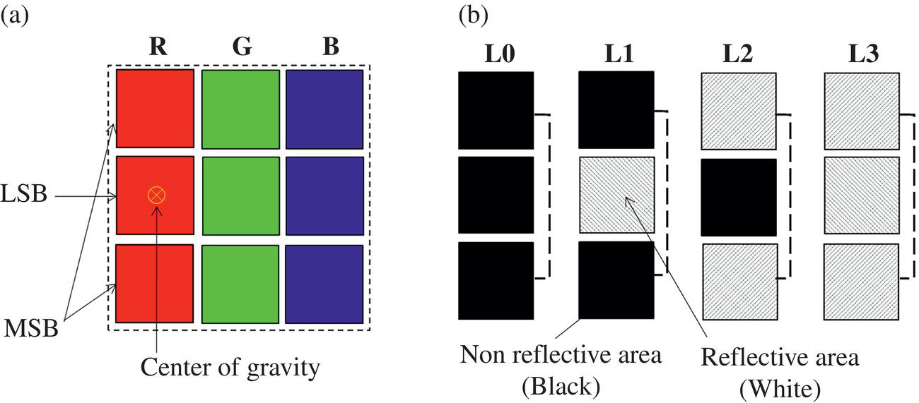
Figure 7.6 (a) “3 divided patterns,” and (b) 2‐bit gradation expressed by “3 divided patterns.”
The following section describes the optical design features of reflective LCDs suitable for MIP LCDs.
7.4 Reflective LCD Optical Design
Development of active‐matrix color‐reflective LCDs occurred in the 1990s [9], and portable game consoles and personal digital assistants (PDAs) with this technology were commercialized in the late 1990s. However, smartphones have replaced these applications with high image quality transmissive LCDs or organic light‐emitting Diodes (OLEDs) during the 2010s. MIP reflective LCDs utilize the technology and manufacturing resources that were established in the 2000s.
A reflective LCD needs to have light scattering functionality because, without this property, it looks like a mirror. The light‐scattering properties have to be optimized depending on how customers use the products, such as the ambient light condition and the viewing angle range. The voltage‐reflectance (V‐R) curve needs to be optimized for MIP digital driving to achieve super low power operations. Auxiliary lighting is required in dark environments. The following section describes the technology to address these issues.
7.4.1 Light Scattering Functionality
There are 2 methods used to add light scattering functionality in the market available MIP reflective LCDs. One is by scattering reflective electrodes [9–11], and the other uses a light control film on the front of the LCD cell [6, 7, 12]. Achieving enough reflectance at the appropriate viewing angle range is the most important design issue for reflective LCDs.
Figure 7.7 illustrates the structure of a color reflective LCD with scattering reflective electrodes. The microstructures under the reflective electrodes are fabricated using a conventional photolithography process. The pattern pitch and shape of the microstructures are controlled by the mask design and process conditions.
Figure 7.8 illustrates the structure of a color reflective LCD with a light control film. A light control film, which has an asymmetric scattering feature controlled by random internal structures with different refractive indices [13], is put on the front side of the LC. This design makes it possible to get desirable anisotropic scattering properties [6, 7, 12].

Figure 7.7 Structure of a color reflective LCD with scattering reflective electrodes.
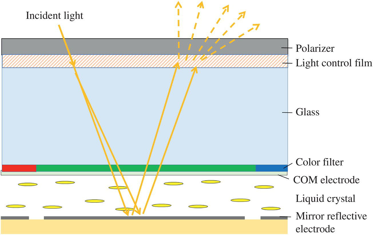
Figure 7.8 Structure of a color reflective LCD with a light control film.
The scattering reflective electrodes method is advantageous for high‐resolution LCDs to avoid image blurring issues because its scattering function is in the LC. However, it is challenging to obtain anisotropic scattering properties. Moreover, it also has a tendency to show rainbow diffraction patterns under sunlight caused by the periodic pattern of the microstructure.
A light control film method can achieve high reflectivity at a specified viewing angle range without causing rainbow diffraction patterns. On the other hand, this method is unsuitable for larger LCDs because this specified viewing angle range is recognized as gradation of reflectance. Image blurring, which is dependent on the pixel pitch versus the color filter glass thickness, is another issue for high‐resolution devices. Practically, it is not an issue for MIP reflective LCDs because MIP circuits have more stringent limitations to achieve high levels of resolution.
The following section describes a LC and an optical design suitable for MIP reflective LCDs.
7.4.2 LCD Cell Design
Electrically controlled birefringence (ECB) and vertical alignment (VA) modes are widely used for reflective and transflective LCDs [5–7,9–12]. Both modes have been used in currently market‐available MIP reflective LCDs. Figure 7.9 shows a basic example of an optical switching mechanism corresponding to both ECB normally white and VA normally black reflective modes. Unpolarized ambient light changes to linearly polarized light after passing through the polarizer. A wide‐band quarter‐wave plate film (λ/4) is added between the polarizer and the LC cell to avoid light leakage when showing a black image. The LC cell is designed to work as a quarter‐wave (λ/4) optical switch. Since the light passes through the LC layer two times in reflective mode, the reflective LC cell works as a half‐wave optical switch (λ/2). This results in rotating linearly polarized light 90° or not. Thus, it is possible to show black and white images.
VA and ECB normally white modes are advantageous to achieve a high contrast target ratio. The black level of these modes is insensitive to cell gap variation because LC molecules are vertically aligned when showing black (Figure 7.9, left). The ECB mode is advantageous for higher reflectivity and low voltage driving because of its V‐R characteristics.
Since reflective LCDs are not visible in a dark environment, the necessity of auxiliary lighting remains unchanged. It is not ideal to sacrifice reflective electrodes and MIP circuit areas to minimize the operating time of auxiliary light. The following section describes the challenge of adding an auxiliary lighting function.
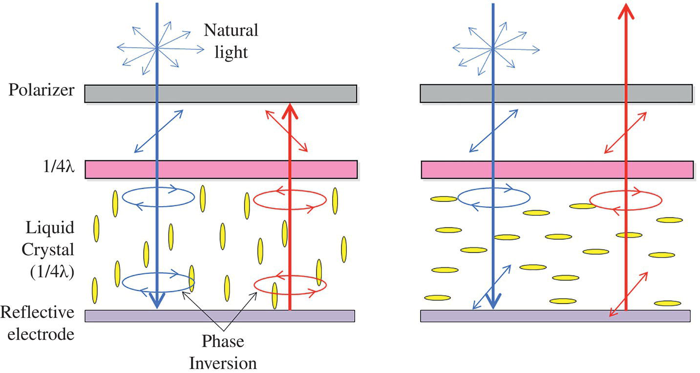
Figure 7.9 Reflective optical switching mechanism of ECB and VA mode LCDs.
7.4.3 Pixel Design for Auxiliary Lighting
There are two ways to add auxiliary lighting. One is by adding front‐light, and the other is backlight. Front lighting is considered an excellent way to light reflective displays because it does not sacrifice reflectivity. Reflective LCDs with front‐light were introduced in the 2000s, but they were soon replaced by transflective LCDs with backlight because of the poor reflective image quality and the manufacturing and module design issues associated with front‐lights. Backlighting is better because backlight technologies are now well‐established and are readily available. However, securing the transmissive area without sacrificing reflective areas is the biggest challenge.
Figure 7.10 shows a cross‐sectional diagram of a conventional transflective LCD pixel, which is composed of a dual cell gap normally black ECB mode [7]. The retardation of the transmissive area is set to 2/λ, while the reflective area is set to 4/λ to coincide the voltage dependence on transmittance (V‐T) with the reflectance (V‐R). Since the transmissive area is put inside the pixel electrode, there is an inevitable trade‐off between the reflectance and the transmittance. This design utilizes signal and gate lines for light‐shielding layers in transmissive mode to achieve a higher contrast ratio target.

Figure 7.10 Cross sectional diagram of a conventional transflective LCD pixel.

Figure 7.11 Cross sectional diagram of a MIP reflective LCD pixel.
Figure 7.11 shows a cross‐sectional diagram of a MIP reflective LCD pixel, composed of a single cell gap normally black ECB mode [7]. The gate and signal lines to drive MIP circuits are set under the pixel electrode as much as possible to avoid LC responses caused by the leakage of their electric fields. Hence, the inter‐pixel areas can be utilized as transmissive areas. This approach makes it possible to keep transmissive areas without sacrificing any reflective areas. The directions of LC molecules on the inter‐pixel area are controlled by the fringe field from the adjacent pixel electrodes. A normally‐black mode is inevitable for this approach to avoid uncontrolled LC molecules causing light leakage when displaying a black image.
As shown in Figure 7.11, a single‐cell gap LC cell is employed for this approach. Figure 7.12 shows the typical V‐R and V‐T curves of a single gap ECB normally black LCD, which is applied to commercially available MIP reflective LCDs. The V‐T curve is not saturated in this voltage range because the cell gap is not optimized for the transmissive mode. The compatibility of V‐R and V‐T curves is a big issue for conventional active‐matrix transflective LCDs. However, the area coverage modulation method utilizes only black and white states, which is not critical for MIP reflective LCDs.
Figure 7.13 illustrates a schematic diagram of 2‐bit gradation in transmissive mode expressed by the fringe of the 3 divided sub‐pixel electrodes, where k denotes the length of one side of a square of a divided pixel electrode. Since the directions of the LC molecules of the transmissive area are controlled by the fringe field of the divided pixel electrodes, transmittance of each sub‐pixel is proportional to the perimeter of the white pixel electrodes [7].
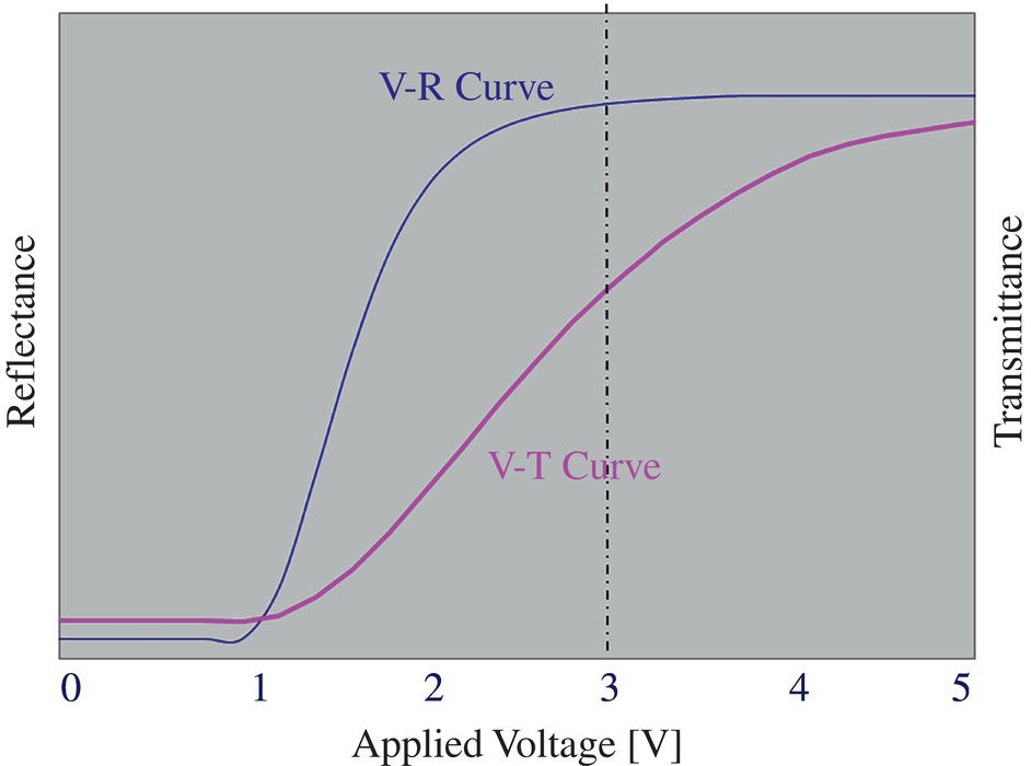
Figure 7.12 Typical V‐R and V‐T curves of a single gap ECB normally‐black LCD.
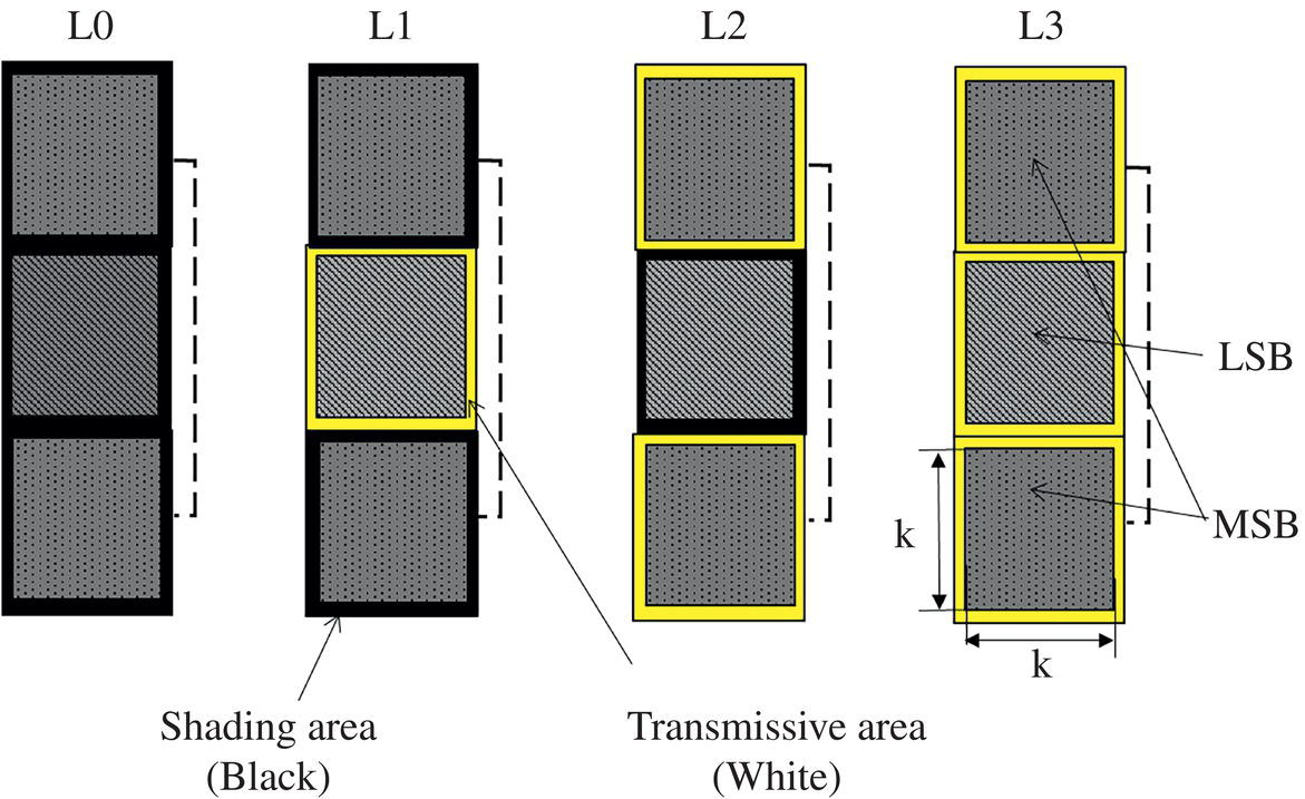
Figure 7.13 2‐bit gradation expressed by the fringe of the pixel electrode.
Table 7.1 lists the area, the perimeter, and the ratios of LSB and MSB for the “3 divided patterns.” LSB/MSB ratios for both the area and the perimeter are 0.5. The “3 divided patterns” design is suitable for reflective mode and transmissive mode to express 2‐bit gradation [7].
As described in the previous section, MIP LCD consumes only a small amount of charging and discharging current to the LC capacitor at low frequency to avoid flickering and image sticking. Power consumption (P) is estimated by
It is desirable to drive LC at low voltage and low frequency as much as possible. From the viewpoint of low voltage driving, ECB mode is more advantageous when compared with VA mode. If the power consumption is the number one priority, then ECB mode is the best choice.
The MIP reflective LCD pixel design has major advantages in preventing flickering and image sticking issues compared with a conventional active‐matrix LCD pixel design. Since LC pixels of MIP LCDs are driven by static voltage, we do not need to consider a TFT leak current and voltage holding ratio of the LC. Furthermore, each LC subpixel is shown in only a black or a white state.
Figure 7.12 shows the V‐R curve of an ECB normally black LCD. Since the V‐R curve is fully saturated at 3 V, COM frequency can be reduced to 0.5 Hz without any issues. On the other hand, flickering is observed in VA mode at the same VCOM frequency because the V‐R curve is not saturated at 3 V.
The coincidence of V‐R and V‐T curves is not an issue for the area coverage modulation method, but avoiding flickering issues in transmissive mode is problematic. The driving method to solve this issue is described below.
Table 7.1 The area and the perimeter of LSB and MSB for “3 divided patterns.”
| LSB | MSB | LSB/MSB | |
|---|---|---|---|
| Area | k2 | 2k2 | 1/2 |
| Perimeter | 4k | 8k | 1/2 |

Figure 7.14 VCOM driving method to avoid flickering issue with backlight.
7.4.4 Super Low Power Driving for Auxiliary Lighting
Flickering and image sticking issues are caused by an offset voltage of the LC cell. The main causes are the difference between the LC interface potential on the COM electrode and on the reflective electrode, including the charge‐up of the LC. The V‐T curve in Figure 7.12 shows that the transmittance is sensitive to the voltage shift at the driving voltage (3 V). So, flickering is easily observable in transmissive mode.
Figure 7.14 shows the driving method to avoid flickering issues in transmissive mode while keeping ultra‐super low power operation in reflective mode. Human eyes recognize flickering light as continuous light when the frequency is higher than the “flicker fusion threshold,” around 50–60 Hz. Flickering issues can be avoided by changing the VCOM frequency to synchronize with the lighting period. This driving method has been applied to wearable devices, which can be powered by a button battery with the battery lasting for up to one year without charge.
As described in the previous section, MIP LCD is limited in the number of colors it can display. The following section shows how to display natural images with limited colors.
7.5 How to Show a Natural Image
There is an intrinsic problem for the MIP LCDs' image quality deteriorates when converting full‐color data to lower bit color data. This section describes the method to show natural images with limited color bits.

Figure 7.15 Comparison of how color depth reduction and error diffusion processes affect image quality.
The error diffusion and dithering methods are widely used when reducing color depth [14, 15]. Figure 7.15 shows how color depth reduction and error diffusion processes affect an image. When the original image with 24‐bit (8‐bit/color) is converted to a 6‐bit (2‐bit/color) by discarding the lower 6‐bit/color, large flat areas and the loss of detail are noticeable. To minimize the deterioration in image quality, error diffusion or dithering data processing is required before sending data to the MIP. Figure 7.16c depicts the 6‐bit (2‐bit/color) image after applying the Floyd‐Steinberg dithering method for error diffusion. As seen in the figure, the image quality is enhanced with this method. However, fluttering is an issue when showing moving images. Ordered dithering is necessary for moving images. While the image quality processed by ordered dithering is slightly inferior to images created by error diffusion, the difference is less perceptible, especially when images are changed successively.
The following section introduces the specifications of selected market available MIP reflective LCD devices and the driving method to achieve super low power operations.
7.6 Design Characteristics of Current Market‐Available Products and Their Super Low Power Operations
Figure 7.16 shows a picture and key specifications of a 1.2 in. 240 × 240 2‐bit/color MIP reflective LCD. The difference between the circumradius and the active area, which is the most critical parameter to achieve narrow border watch design, is only 2.4 mm. Thanks to the small number of input pins and lack of driver IC, the FOG pad size is small enough to achieve a small border size. The LCD module consists of LCD glass, front and rear polarizers, and an FPC without a component. The display interface is a parallel interface with 6 data bus lines customized for MIP LCD design. When all gate lines are refreshed, the maximum refresh rate is 30 fps. The power consumption needed to show a static image is only 4 μW. This design architecture is widely used for GPS sports watches because of the narrow border design and adequate maximum refresh rate.

Figure 7.16 Picture and key specifications of a 1.2 in. 240 × 240 2bit/color MIP reflective LCD.

Figure 7.17 Picture and key specifications of a 1.04″ 208 × 208 1‐bit/color MIP reflective LCD.
Figure 7.17 shows a picture and key specifications of a 1.04″ 208 × 208 1‐bit/color MIP reflective LCD. The LCD module consists of LCD glass, front and rear polarizers, and an FPC without a component. The display interface is a Serial Peripheral Interface (SPI), one of the simplest display interfaces, which almost all super low power microcontrollers (MCUs) support. The interface includes four control signals (SCS, SCK, SI, DISP), one data signal (SI), and one VCOM timing control signal (COMIN), and it can be driven by a single power source (3 V). When all gate lines are refreshed, the maximum refresh rate is 10 fps. The power consumption needed to show a static image is only 3 μW.
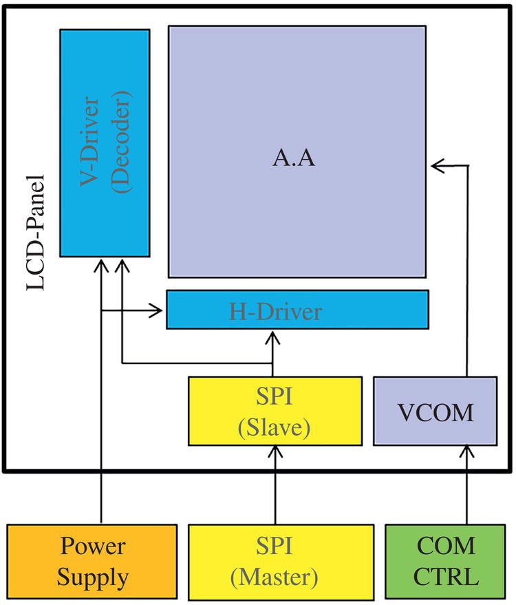
Figure 7.18 System block diagram of a 1.04″ 208 × 208 1‐bit/color MIP LCD.
Figure 7.18 shows a system block diagram of a 1.04″ 208 × 208 1‐bit/color MIP LCD. It has a SPI(Slave) and a VCOM driving signal generator on the glass border. All the commands and data are sent directly from an MCU that supports SPI. Received SPI commands and data are processed in the SPI circuit and the decoder, located on the border area. Because of the SPI and single 3 V power supply features, this system architecture is used for activity trackers powered by a coin battery without charging.
Figure 7.19 shows how VCOM/FRP and XFRP signals are generate from the COMIN input signal in LCD. A timing signal is needed to change the polarity of the VCOM/FRP and XFRP (COMIN).
Since a MIP LCD can be driven directly from MCU, reducing the power to generate control signals in an MCU is important to achieve super low power as a system. Since a MIP LCD stores display image data in the active area, only the voltage supply to keep SRAMs working and COMIN signal to toggle LC polarity is required (Figures 7.2, 7.3, and 7.19) when displaying a still image. This means that the MCU can go into sleep mode when displaying a still image. It is important to reduce the power consumption to generate the COMIN signal. Recently, every electronic device has included a super low‐power real time clock (RTC) circuit. By utilizing the RTC output to generate a COMIN signal, MIP reflective LCDs can be lit at super low power as a system.
Figure 7.20 shows how to generate a COMIN signal from RTC output. Every RTC has a 32.768 kHz oscillator and frequency dividers to count seconds. By utilizing these circuits, COMIN timing can be generated at ultra‐super low power consumption.
Super low power consumption is a key feature of MIP LCDs. This feature is summarized in the following section.
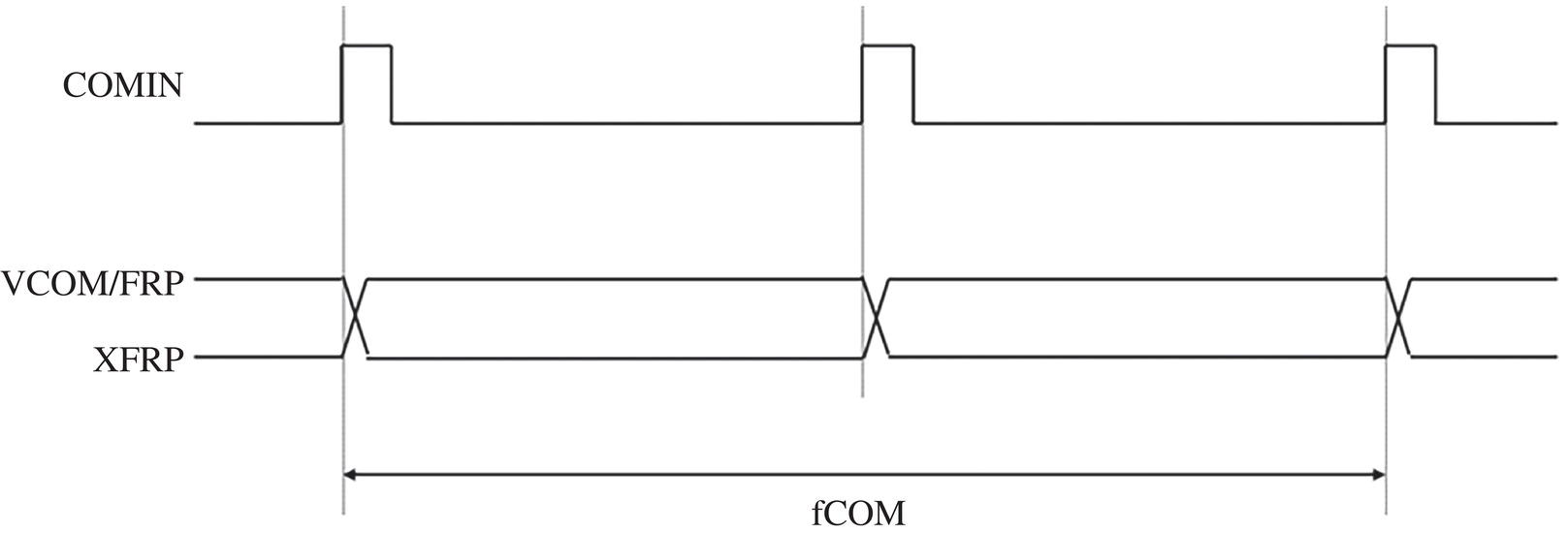
Figure 7.19 VCOM/FRP and XFRP signals generated in LCD from COMIN input signal.
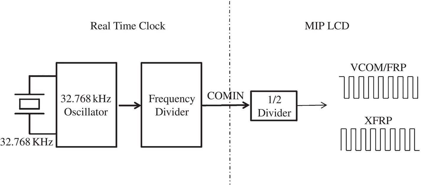
Figure 7.20 VCOM control signal generated by real time clock circuits to drive MIP reflective LCD.
7.7 Summary of Power Consumption
Figure 7.21 shows power consumption levels of both transmissive LCD and reflective LCDs, with and without MIP. Large amounts of a transmissive LCD's power are consumed by the backlight. Reflective LCDs utilize environmental light and have no need for a lit backlight when the environment is bright enough. Under the same conditions as described in Figure 7.16, 1.2 in. 240 × 240, the power consumption of a conventional active‐matrix transmissive LCD fabricated by the LTPS process is estimated to be around 50 mW, of which 20% (10 mW) is consumed for data refreshing through the driver IC, and 80% (40 mW) is consumed for backlight. A conventional active‐matrix LCD equips a driver IC to generate voltages and timing signals to operate the H‐driver, V‐driver, and COM driver, as well as analog signals to drive signal lines. The majority of the power consumed in the driver IC is used to generate these signals and voltages. The MIP reflective LCD described in Figure 7.16 consumes only 160 μW for a 30 fps moving picture and 4 μW for a still image. A MIP reflective LCD is controlled directly from an MCU. The MCU engine can go into sleep mode when displaying a still image. However, a VCOM toggling timing signal is needed even when displaying a still image. To generate this VCOM toggling timing, power consumption can be reduced by utilizing low‐power RTC signals. MIP reflective LCD's power consumption is less than 1% of conventional transmissive LCDs when displaying still images.
The following section describes how MIP reflective LCD technology has been applied to devices in the market.
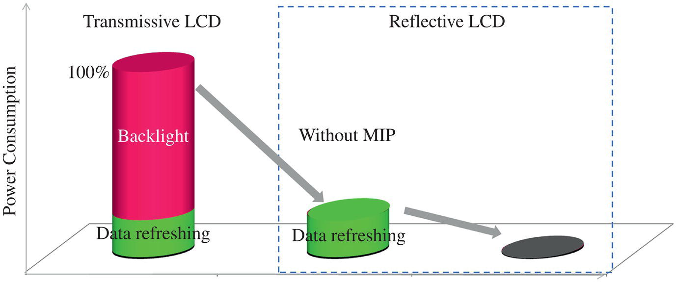
Figure 7.21 Power consumption comparison of transmissive LCD, and reflective LCDs with and without MIP.
7.8 Applications
The main features of the MIP reflective LCDs include:
- Super‐low power operation
- Outdoor visibility
- Capability of showing moving images
- Simple structure: LCD glass + Front and rear polarizer + FPC
By utilizing these properties, color MIP reflective LCDs have been used for GPS‐equipped sports watches, wristbands, and smartwatches, from 2013 onwards. Other technology applications that include larger displays are cycle computers and golf carts.
However, smart watches that use ‐OLED technology are now challenging MIP reflective LCDs for market share due to their excellent optical properties. “Always‐on display” is the “new normal” for smartwatches. The power consumption of an OLED wearable display when displaying a watch face is several milliwatts. This is lower than conventional transmissive LCDs, but far bigger than MIP reflective LCDs. Moreover, smartwatches equipped with always‐on OLED displays need to be charged daily.
Recently, due to increased awareness of the need for health management monitoring, watches are being modified to include health care applications that monitor step count, walking distance, heart rate, blood oxygen levels, stress levels, and sleep patterns. From a design viewpoint, current smartwatches tend to be too bulky to be worn 24/7. The largest component inside the smartwatch case is the battery. With super low power technology, it is possible to reduce the watch size by reducing the battery size dramatically, keeping the frequency of charging to over one week.
Due to their super‐low power characteristics, MIP reflective LCDs are suitable for 24/7 health monitoring devices.
The following section previews future possibilities for this technology.
7.9 Future Expectations
Display technology has evolved to improve image quality, offering high definition, high color gamut, high contrast ratio, and wide viewing angle. Mobile communication technology and application processor of handsets have also been developed to improve data transfer and processing rates with the growth of the smartphone market. While low power consumption is important, mobile devices have not been the first priority. People are accustomed to having to charge their mobile devices every day. As a result, transmissive LCD and OLED are now the main players in the display market.
With the expectation of Internet of Things (IoT) technologies, infrastructure for low power communication is becoming a reality. Bluetooth low energy (BLE) has already been widely used in many applications of IoT. Low power wide area network (LPWAN) services are now availabl enabling devices to communicate over large geographical areas where power supply cables are unavailable. Ultra‐super low‐power MCUs incorporating BLE functionality have been available for the last decade. Recently, software development kits (SDK) with LPWAN connectivity have been released.
As more devices connect to the internet at low power communication, the sensor data, including environmental data, human activity (e.g., position, motion, and health data), and pictorial images and information interpreted from the images are all reported the internet. The data are analyzed by artificial intelligence (AI) utilized in human behavior analysis and abnormality detection. Accumulating and utilizing these data by AI makes it possible to efficiently allocate human and social resources. For example, individual health data can now be automatically analyzed and sent to medical health specialists directly, which improves the quality and timeliness of health advice.
Super low power displays are necessary to interface humans with IoT edge devices that report sensor data. With LTPS SOG technologies, it is possible to incorporate various sensor features on the glass, such as ambient light sensors, in‐cell touch sensors, and fingerprint or finger vein recognition functions. A MIP reflective LCD for a wearable device consumes only several microwatts of power to show an image, and it can be lit by the power generated by a solar cell incorporated in the watch.
We believe that MIP reflective LCD technology will play an important role in the development of the IoT market in the future.
References
- 1 Kimura, H., Maeda, T., Tsunashima, T. et al. (2001). A 2.15‐in. QCIF reflective color TFT‐LCD with digital memory on glass (DMOG). SID Symp. Digest. 32: 268–271.
- 2 Senda, M., Tsutsui, Y., Sasaki, A. et al. (2003). Ultra‐low‐power polysilicon AMLCD with full integration. J. Soc. Inf. Disp. 11: 121–125.
- 3 Nakajima, Y., Teranishi, Y., Kida, Y., and Maki, Y. (2006). Ultra‐low power LTPS TFT‐LCD technology using a multi‐bit pixel memory circuit. J. Soc. Inf. Disp. 14: 1071–1075.
- 4 Harada, K., Kimura, H., Miyatake, M. et al. (2009). A novel low‐power‐consumption all‐digital system‐on‐glass display with serial interface. SID Symp. Digest. 40: 383–386.
- 5 Fukunaga, Y., Shima, T., Nakao, T., Teranishi, Y., Nakajima, Y. (2015). Ultra‐low power reflective LCD technology and its application for wearable devices. AM‐FPD. Digest. 209–212.
- 6 Fukunaga, Y., Tamaki, M., Mitsui, M. et al. (2013). Low power, high image quality color reflective LCDs realized by memory‐in‐pixel technology and optical optimization using newly‐developed scattering layer. SID Symp. Digest. 44: 701–704.
- 7 Tamaki, M., Fukunaga, Y., Mitsui, M. et al. (2015). A memory‐in‐pixel reflective‐type LCD using newly designed system and pixel structure. J. Soc. Inf. Disp. 22: 251–259.
- 8 Nanno, Y., Senda, K., Tsutsu, H. (2001). Image analysis of area ratio gray scale method for active‐matrix LCDs. Proc. IDW ’01. 419–422.
- 9 Uchida, T. (1995). Trend of reflective color liquid crystal displays. AM‐LCD‘95. 23–26.
- 10 Kubo, M., Ochi, T., Narutaki, Y. et al. (2000). Development of “Advanced TFT‐LCD” with good legibility under any ambient light intensity. J. Soc. Inf. Disp. 8 (4): 299–304.
- 11 Kimura, N. (2001). High‐performance reflective TFT‐LCD. Proc. AM‐LCD’01. 55–58.
- 12 T. Ishinabe and T. Uchida. (2008). A bright and wide color gamut reflective full‐color LCD using diffused light control technology. Proceedings of International Meeting on Information Display. 1377–1380.
- 13 Honda, M., Hozumi, S., and Kitayama, S. (1993). A novel polymer film that controls light transmission. Prog. Polym. Sci. 3: 159–169.
- 14 Floyd, R. W. and Steinberg, L. (1976). An Adaptive Algorithm for Spatial Grayscale. Proceedings of the Society of Information Display. 17 (2): 75–77.
- 15 Bayer, B. (1973). An optimum method for two‐level rendition of continuous‐tone pictures. IEEE Int. Conf. on Communications. 11–15.