2.3 ARM Processor
In this section, we concentrate on the ARM processor. ARM is actually a family of RISC architectures that have been developed over many years. ARM does not manufacture its own chips; rather, it licenses its architecture to companies who either manufacture the CPU itself or integrate the ARM processor into a larger system.
The textual description of instructions, as opposed to their binary representation, is called an assembly language. ARM instructions are written one per line, starting after the first column. Comments begin with a semicolon and continue to the end of the line. A label, which gives a name to a memory location, comes at the beginning of the line, starting in the first column:
LDR r0,[r8] ; a comment
label ADD r4,r0,r1W
2.3.1 Processor and Memory Organization
Different versions of the ARM architecture are identified by number. ARM7 is a von Neumann architecture machine, while ARM9 uses a Harvard architecture. However, this difference is invisible to the assembly language programmer except for possible performance differences.
The ARM architecture supports two basic types of data:
ARM7 allows addresses to be 32 bits long. An address refers to a byte, not a word. Therefore, the word 0 in the ARM address space is at location 0, the word 1 is at 4, the word 2 is at 8, and so on. (As a result, the PC is incremented by 4 in the absence of a branch.) The ARM processor can be configured at power-up to address the bytes in a word in either little-endian or big-endian mode, as shown in Figure 2.7.
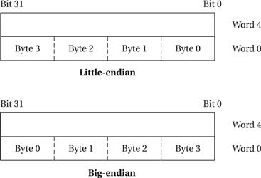
Figure 2.7 Byte organizations within an ARM word.
General-purpose computers have sophisticated instruction sets. Some of this sophistication is required simply to provide the functionality of a general computer, while other aspects of instruction sets may be provided to increase performance, reduce code size, or otherwise improve program characteristics. In this section, we concentrate on the functionality of the ARM instruction set.
2.3.2 Data Operations
Arithmetic and logical operations in C are performed in variables. Variables are implemented as memory locations. Therefore, to be able to write instructions to perform C expressions and assignments, we must consider both arithmetic and logical instructions as well as instructions for reading and writing memory.
Figure 2.8 shows a sample fragment of C code with data declarations and several assignment statements. The variables a, b, c, x, y, and z all become data locations in memory. In most cases data is kept relatively separate from instructions in the program’s memory image.
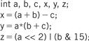
Figure 2.8 A C fragment with data operations.
ARM programming model
In the ARM processor, arithmetic and logical operations cannot be performed directly on memory locations. While some processors allow such operations to directly reference main memory, ARM is a load-store architecture—data operands must first be loaded into the CPU and then stored back to main memory to save the results. Figure 2.9 shows the registers in the basic ARM programming model. ARM has 16 general-purpose registers, r0 through r15. Except for r15, they are identical—any operation that can be done on one of them can be done on the others. The r15 register has the same capabilities as the other registers, but it is also used as the program counter. The program counter should of course not be overwritten for use in data operations. However, giving the PC the properties of a general-purpose register allows the program counter value to be used as an operand in computations, which can make certain programming tasks easier.

Figure 2.9 The basic ARM programming model.
The other important basic register in the programming model is the current program status register (CPSR). This register is set automatically during every arithmetic, logical, or shifting operation. The top four bits of the CPSR hold the following useful information about the results of that arithmetic/-logical operation:
• The negative (N) bit is set when the result is negative in two’s-complement arithmetic.
• The zero (Z) bit is set when every bit of the result is zero.
• The carry (C) bit is set when there is a carry out of the operation.
• The overflow (V) bit is set when an arithmetic operation results in an overflow.
These bits can be used to easily check the results of an arithmetic operation. However, if a chain of arithmetic or logical operations is performed and the intermediate states of the CPSR bits are important, they must be checked at each step because the next operation changes the CPSR values.
Example 2.1 illustrates the computation of CPSR bits.
Example 2.1 Status Bit Computation in the ARM
An ARM word is 32 bits. In C notation, a hexadecimal number starts with 0x, such as 0xffffffff, which is a two’s-complement representation of −1 in a 32-bit word.
Here are some sample calculations:
The basic form of a data instruction is simple:
ADD r0,r1,r2
This instruction sets register r0 to the sum of the values stored in r1 and r2. In addition to specifying registers as sources for operands, instructions may also provide immediate operands, which encode a constant value directly in the instruction. For example,
ADD r0,r1,#2
sets r0 to r1 + 2.
The major data operations are summarized in Figure 2.10. The arithmetic operations perform addition and subtraction; the with-carry versions include the current value of the carry bit in the computation. RSB performs a subtraction with the order of the two operands reversed, so that RSB r0,r1,r2 sets r0 to be r2 – r1. The bit-wise logical operations perform logical AND, OR, and XOR operations (the exclusive or is called EOR). The BIC instruction stands for bit clear: BIC r0,r1,r2 sets r0 to r1 and not r2. This instruction uses the second source operand as a mask: Where a bit in the mask is 1, the corresponding bit in the first source operand is cleared. The MUL instruction multiplies two values, but with some restrictions: No operand may be an immediate, and the two source operands must be different registers. The MLA instruction performs a multiply-accumulate operation, particularly useful in matrix operations and signal processing. The instruction
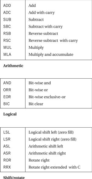
Figure 2.10 ARM data instructions.
MLA r0,r1,r2,r3
sets r0 to the value r1 × r2 + r3.
The shift operations are not separate instructions—rather, shifts can be applied to arithmetic and logical instructions. The shift modifier is always applied to the second source operand. A left shift moves bits up toward the most-significant bits, while a right shift moves bits down to the least-significant bit in the word. The LSL and LSR modifiers perform left and right logical shifts, filling the least-significant bits of the operand with zeroes. The arithmetic shift left is equivalent to an LSL, but the ASR copies the sign bit—if the sign is 0, a 0 is copied, while if the sign is 1, a 1 is copied. The rotate modifiers always rotate right, moving the bits that fall off the least-significant bit up to the most-significant bit in the word. The RRX modifier performs a 33-bit rotate, with the CPSR’s C bit being inserted above the sign bit of the word; this allows the carry bit to be included in the rotation.
The instructions in Figure 2.11 are comparison operands—they do not modify general-purpose registers but only set the values of the NZCV bits of the CPSR register. The compare instruction CMP r0, r1 computes r0 – r1, sets the status bits, and throws away the result of the subtraction. CMN uses an addition to set the status bits. TST performs a bit-wise AND on the operands, while TEQ performs an exclusive-or.

Figure 2.11 ARM compare instructions.
Figure 2.12 summarizes the ARM move instructions. The instruction MOV r0,r1 sets the value of r0 to the current value of r1. The MVN instruction complements the operand bits (one’s complement) during the move.
![]()
Figure 2.12 ARM move instructions.
Values are transferred between registers and memory using the load-store instructions summarized in Figure 2.13. LDRB and STRB load and store bytes rather than whole words, while LDRH and SDRH operate on half-words and LDRSH extends the sign bit on loading. An ARM address may be 32 bits long. The ARM load and store instructions do not directly refer to main memory addresses, because a 32-bit address would not fit into an instruction that included an opcode and operands. Instead, the ARM uses register-indirect addressing. In register-indirect addressing, the value stored in the register is used as the address to be fetched from memory; the result of that fetch is the desired operand value. Thus, as illustrated in Figure 2.14, if we set r1 = 0x100, the instruction

Figure 2.13 ARM load-store instructions and pseudo-operations.
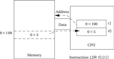
Figure 2.14 Register indirect addressing in the ARM.
LDR r0,[r1]
sets r0 to the value of memory location 0x100. Similarly, STR r0,[r1] would store the contents of r0 in the memory location whose address is given in r1. There are several possible variations:
LDR r0,[r1, – r2]
loads r0 from the address given by r1 – r2, while
LDR r0,[r1, #4]
loads r0 from the address r1 + 4.
This begs the question of how we get an address into a register—we need to be able to set a register to an arbitrary 32-bit value. In the ARM, the standard way to set a register to an address is by performing arithmetic on a register. One choice for the register to use for this operation is the program counter. By adding or subtracting to the PC a constant equal to the distance between the current instruction (i.e., the instruction that is computing the address) and the desired location, we can generate the desired address without performing a load. The ARM programming system provides an ADR pseudo-operation to simplify this step. Thus, as shown in Figure 2.15, if we give location 0x100 the name FOO, we can use the pseudo-operation

Figure 2.15 Computing an absolute address using the PC.
ADR r1,FOO
to perform the same function of loading r1 with the address 0x100. Another technique is used in high-level languages like C. As we will see when we discuss procedure calls, languages use a mechanism called a frame to pass parameters between functions. For the moment, a simplified view of the process is sufficient. A register holds a frame pointer (fp) that points to the top of the frame; elements within the frame are accessed using offsets from fp. The assembler syntax [fp,#-n] is used to take the nth location from fp.
Example 2.2 illustrates how to implement C assignments in ARM instruction.
Example 2.2 C Assignments in ARM Instructions
We will use the assignments of Figure 2.8. The semicolon (;) begins a comment after an instruction, which continues to the end of that line. The statement
x = (a + b) − c;
can be implemented by using r0 for a, r1 for b, r2 for c, and r3 for x. We also need registers for indirect addressing. In this case, we will reuse the same indirect addressing register, r4, for each variable load. The code must load the values of a, b, and c into these registers before performing the arithmetic, and it must store the value of x back to memory when it is done.
Here is code generated by the gcc compiler for this statement. It uses a frame pointer to hold the variables: a is at −24, b at −28, c at −32, and x at −36:
ldr r2, [fp, #-24]
ldr r3, [fp, #-28]
add r2, r2, r3
ldr r3, [fp, #-32]
rsb r3, r3, r2
str r3, [fp, #-36]
The operation
y = a*(b + c);
can be coded similarly, but in this case we will reuse more registers by using r0 for both a and b, r1 for c, and r2 for y. Once again, we will use r4 to store addresses for indirect addressing. The resulting code from gcc looks like this:
ldr r2, [fp, #–28]
ldr r3, [fp, #–32]
add r2, r2, r3
ldr r3, [fp, #–24]
mul r3, r2, r3
str r3, [fp, #–40]
The C statement
z = (a << 2) | (b & 15);
results in this gcc-generated code:
ldr r3, [fp, #–24]
mov r2, r3, asl #2
ldr r3, [fp, #–28]
and r3, r3, #15
orr r3, r2, r3
str r3, [fp, #–44]
More addressing modes
We have already seen three addressing modes: register, immediate, and indirect. The ARM also supports several forms of base-plus-offset addressing, which is related to indirect addressing. But rather than using a register value directly as an address, the register value is added to another value to form the address. For instance,
LDR r0,[r1,#16]
loads r0 with the value stored at location r1 + 16. Here, r1 is referred to as the base and the immediate value the offset. When the offset is an immediate, it may have any value up to 4,096; another register may also be used as the offset. This addressing mode has two other variations: auto-indexing and post-indexing. Auto-indexing updates the base register, such that
LDR r0,[r1,#16]!
first adds 16 to the value of r1, and then uses that new value as the address. The ! operator causes the base register to be updated with the computed address so that it can be used again later. Our examples of base-plus-offset and auto-indexing instructions will fetch from the same memory location, but auto-indexing will also modify the value of the base register r1. Post-indexing does not perform the offset calculation until after the fetch has been performed. Consequently,
LDR r0,[r1],#16
will load r0 with the value stored at the memory location whose address is given by r1, and then add 16 to r1 and set r1 to the new value. In this case, the post-indexed mode fetches a different value than the other two examples, but ends up with the same final value for r1 as does auto-indexing.
We have used the ADR pseudo-op to load addresses into registers to access variables because this leads to simple, easy-to-read code (at least by assembly language standards). Compilers tend to use other techniques to generate addresses, because they must deal with global variables and automatic variables.
2.3.3 Flow of Control
The B (branch) instruction is the basic mechanism in ARM for changing the flow of control. The address that is the destination of the branch is often called the branch target. Branches are PC-relative—the branch specifies the offset from the current PC value to the branch target. The offset is in words, but because the ARM is byte-addressable, the offset is multiplied by four (shifted left two bits, actually) to form a byte address. Thus, the instruction
B #100
will add 400 to the current PC value.
We often wish to branch conditionally, based on the result of a given computation. The if statement is a common example. The ARM allows any instruction, including branches, to be executed conditionally. This allows branches to be conditional, as well as data operations. Figure 2.16 summarizes the condition codes.

Figure 2.16 Condition codes in ARM.
We use Example 2.3 as a way to explore the uses of conditional execution.
Example 2.3 Implementing an if Statement in ARM
We will use the following if statement as an example:
if (a > b) {
x = 5;
y = c + d;
}
else x = c - d;
The implementation uses two blocks of code, one for the true case and another for the false case. Let’s look at the gcc-generated code in sections. First, here is the compiler-generated code for the a>b test:
ldr r2, [fp, #-24]
ldr r3, [fp, #-28]
cmp r2, r3
ble .L2
Here is the code for the true block:
.L2: mov r3, #5
str r3, [fp, #-40]
ldr r2, [fp, #-32]
ldr r3, [fp, #-36]
add r3, r2, r3
str r3, [fp, #-44]
b .L3
And here is the code for the false block:
ldr r3, [fp, #-32]
ldr r2, [fp, #-36]
rsb r3, r2, r3
str r3, [fp, #-40]
.L3:
The loop is a very common C statement, particularly in signal processing code. Loops can be naturally implemented using conditional branches. Because loops often operate on values stored in arrays, loops are also a good illustration of another use of the base-plus-offset addressing mode. A simple but common use of a loop is in the FIR filter, which is explained in Application Example 2.1; the loop-based implementation of the FIR filter is described in Example 2.5.
Application Example 2.1 FIR Filters
A finite impulse response (FIR) filter is a commonly used method for processing signals; we make use of it in Section 5.12. The FIR filter is a simple sum of products:
![]() (Eq. 2.1)
(Eq. 2.1)
In use as a filter, the xis are assumed to be samples of data taken periodically, while the cis are coefficients. This computation is usually drawn like this:
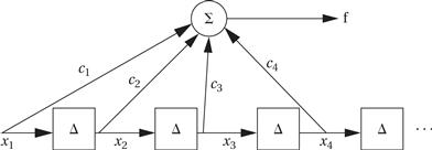
This representation assumes that the samples are coming in periodically and that the FIR filter output is computed once every time a new sample comes in. The Δ boxes represent delay elements that store the recent samples to provide the xi s. The delayed samples are individually multiplied by the ci s and then summed to provide the filter output.
Example 2.5 An FIR Filter for the ARM
Here is the C code for an FIR filter:
for (i = 0, f = 0; i < N; i++)
f = f + c[i] * x[i];
We can address the arrays c and x using base-plus-offset addressing: We will load one register with the address of the zeroth element of each array and use the register holding i as the offset.
Here is the gcc-generated code for the loop:
.LBB2:
mov r3, #0
str r3, [fp, #-24]
mov r3, #0
str r3, [fp, #-28]
.L2:
ldr r3, [fp, #-24]
cmp r3, #7
ble .L5
b .L3
.L5: ldr r3, [fp, #-24]
mvn r2, #47
mov r3, r3, asl #2
sub r0, fp, #12
add r3, r3, r0
add r1, r3, r2
ldr r3, [fp, #-24]
mvn r2, #79
mov r3, r3, asl #2
sub r0, fp, #12
add r3, r3, r0
add r3, r3, r2
ldr r2, [r1, #0]
ldr r3, [r3, #0]
mul r2, r3, r2
ldr r3, [fp, #-28]
add r3, r3, r2
str r3, [fp, #–28]
ldr r3, [fp, #–24]
add r3, r3, #1
str r3, [fp, #–24]
b .L2
.L3:
The mvn instruction moves the bitwise complement of a value.
C functions
The other important class of C statement to consider is the function. A C function returns a value (unless its return type is void); subroutine or procedure are the common names for such a construct when it does not return a value. Consider this simple use of a function in C:
x = a + b;
foo(x);
y = c − d;
A function returns to the code immediately after the function call, in this case the assignment to y. A simple branch is insufficient because we would not know where to return. To properly return, we must save the PC value when the procedure/function is called and, when the procedure is finished, set the PC to the address of the instruction just after the call to the procedure. (You don’t want to endlessly execute the procedure, after all.)
The branch-and-link instruction is used in the ARM for procedure calls. For instance,
BL foo
will perform a branch and link to the code starting at location foo (using PC-relative addressing, of course). The branch and link is much like a branch, except that before branching it stores the current PC value in r14. Thus, to return from a procedure, you simply move the value of r14 to r15:
MOV r15,r14
You should not, of course, overwrite the PC value stored in r14 during the procedure.
But this mechanism only lets us call procedures one level deep. If, for example, we call a C function within another C function, the second function call will overwrite r14, destroying the return address for the first function call. The standard procedure for allowing nested procedure calls (including recursive procedure calls) is to build a stack, as illustrated in Figure 2.17. The C code shows a series of functions that call other functions: f1() calls f2(), which in turn calls f3(). The right side of the figure shows the state of the procedure call stack during the execution of f3(). The stack contains one activation record for each active procedure. When f3() finishes, it can pop the top of the stack to get its return address, leaving the return address for f2() waiting at the top of the stack for its return.
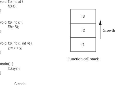
Figure 2.17 Nested function calls and stacks.
Most procedures need to pass parameters into the procedure and return values out of the procedure as well as remember their return address.
We can also use the procedure call stack to pass parameters. The conventions used to pass values into and out of procedures are known as procedure linkage. To pass parameters into a procedure, the values can be pushed onto the stack just before the procedure call. Once the procedure returns, those values must be popped off the stack by the caller, because they may hide a return address or other useful information on the stack. A procedure may also need to save register values for registers it modifies. The registers can be pushed onto the stack upon entry to the procedure and popped off the stack, restoring the previous values, before returning. Procedure stacks are typically built to grow down from high addresses.
Assembly language programmers can use any means they want to pass parameters. Compilers use standard mechanisms to ensure that any function may call any other. (If you write an assembly routine that calls a compiler-generated function, you must adhere to the compiler’s procedure call standard.) The compiler passes parameters and return variables in a block of memory known as a frame. The frame is also used to allocate local variables. The stack elements are frames. A stack pointer (sp) defines the end of the current frame, while a frame pointer (fp) defines the end of the last frame. (The fp is technically necessary only if the stack frame can be grown by the procedure during execution.) The procedure can refer to an element in the frame by addressing relative to sp. When a new procedure is called, the sp and fp are modified to push another frame onto the stack.
The ARM Procedure Call Standard (APCS) [Slo04] is a good illustration of a typical procedure linkage mechanism. Although the stack frames are in main memory, understanding how registers are used is key to understanding the mechanism, as explained below.
• r0-r3 are used to pass the first four parameters into the procedure. r0 is also used to hold the return value. If more than four parameters are required, they are put on the stack frame.
• r4-r7 hold register variables.
• r11 is the frame pointer and r13 is the stack pointer.
• r10 holds the limiting address on stack size, which is used to check for stack overflows.
Other registers have additional uses in the protocol.
Example 2.6 illustrates the implementation of C functions and procedure calls.
Example 2.6 Procedure Calls in ARM
Here is a simple example of two procedures, one of which calls another:
void f2(int x) {
int y;
y = x+1;
}
void f1(int a) {
f2(a);
}
This function has only one parameter, so x will be passed in r0. The variable y is local to the procedure so it is put into the stack. The first part of the procedure sets up registers to manipulate the stack, then the procedure body is implemented. Here is the code generated by the ARM gcc compiler for f2() with manually-created comments to explain the code:
mov ip, sp ; set up f2()’s stack access
stmfd sp!, {fp, ip, lr, pc}
sub fp, ip, #4
sub sp, sp, #8
str r0, [fp, #-16]
ldr r3, [fp, #-16] ; get x
add r3, r3, #1 ; add 1
str r3, [fp, #–20] ; assign to y
ldmea fp, {fp, sp, pc} ; return from f2()
And here is the code generated for f1():
mov ip, sp ; set up f1’s stack access
stmfd sp!, {fp, ip, lr, pc}
sub fp, ip, #4
sub sp, sp, #4
str r0, [fp, #-16] ; save the value of a passed into f1()
ldr r0, [fp, #-16] ; load value of a for the f2() call
bl f2 ; call f2()
ldmea fp, {fp, sp, pc} ; return from f1()
2.3.4 Advanced ARM Features
Several models of ARM processors provide advanced features for a variety of applications.
DSP
Several extensions provide improved digital signal processing. Multiply-accumulate (MAC) instructions can perform a 16 x 16 or 32 x 16 MAC in one clock cycle. Saturation arithmetic can be performed with no overhead. A new instruction is used for arithmetic normalization.
SIMD
Multimedia operations are supported by single-instruction multiple-data (SIMD) operations. A single register is treated as having several smaller data elements, such as bytes. The same operation is simultaneously applied to all the elements in the register.
NEON
NEON instructions go beyond the original SIMD instructions to provide a new set of registers and additional operations. The NEON unit has 32 registers, each 64 bits wide. Some operations also allow a pair of registers to be treated as a 128-bit vector. Data in a single register is treated as a vector of elements, each smaller than the original register, with the same operation being performed in parallel on each vector element. For example, a 32-bit register can be used to perform SIMD operations on 8, 16, 32, 64, or single-precision floating-point numbers.
TrustZone
TrustZone extensions provide security features. A separate monitor mode allows the processor to enter a secure world to perform operations not permitted in normal mode. A special instruction, the secure monitor call, is used to enter the secure world, as can some exceptions.
Jazelle
The Jazelle instruction set allows direct execution of 8-bit Java™ bytecodes. As a result, a bytecode interpreter does not need to be used to execute Java programs.
Cortex
The Cortex collection of processors is designed for compute-intensive applications:
• Cortex-A5 provides Jazelle execution of Java, floating-point processing, and NEON multimedia instructions.
• Cortex-A8 is a dual-issue in-order superscalar processor.
• Cortex-A9 can be used in a multiprocessor with up to four processing elements.
• Cortex-A15 MPCore is a multicore processor with up to four CPUs.
• The Cortex-R family is designed for real-time embedded computing. It provides SIMD operations for DSP, a hardware divider, and a memory protection unit for operating systems.
• The Cortex-M family is designed for microcontroller-based systems that require low cost and low-energy operation.