 CHAPTER 18
Optimization of Image-Processing Algorithms Using FPGAs
Universidad de Extremadura, Spain
A. GÓMEZ
Centro Extremeño de Tecnologias Avanzadas, Spain
J. A. GÓMEZ and J. M. SÁNCHEZ
Universidad de Extremadura, Spain
18.1 INTRODUCTION
At present, FPGAs (field-programmable gate arrays) are very popular devices in many different fields. In particular, FPGAs are a good alternative for many real applications in image processing. Several systems using programmable logic devices have been designed, showing the utility of these devices for artificial-vision applications [1]. Whereas other papers display the results of implementing image-processing techniques by means of “standard” FPGAs or reconfigurable computing systems [2]. In this chapter we present the implementation and optimization of 16 image-processing operations by means of reconfigurable hardware. Our FPGA implementations use several parallelism techniques, include other optimizations as we will see, and have high operation frequencies. Thanks to all this, they obtain very good results. In fact, our FPGA-based implementations are even more than 149 times faster than the corresponding software implementation.
The chapter is organized as follows. In Section 18.2 we give a brief background about the use of FPGAs for optimizing image-processing algorithms. In Section 18.3 we describe the main characteristics of our FPGA-based image-processing operations. In Section 18.4 we give more details about the types of algorithms we use in our hardware implementations. Then we present a number of comparisons between the software and FPGA-based implementations, and finally, conclusions are given in Section 18.6.
18.2 BACKGROUND
Vision has been the center of attention for researchers from the beginnings of computing since it is the most notorious perception mechanism for human beings. Research into the emulation of visual capability by means of computers has been developed to such an extent that, at present, vision plays a very important role in many application fields, from medical imaging to factory automation in robotics; and it is a key discipline in the general objective of allowing machines to “understand” the world.
Generally, a computer vision system extracts quantitative information from an image through the following steps: image acquisition, manipulation, understanding, and decision making (actuation), the last three which can be performed by a computer. On the other hand, the image manipulation and understanding steps are carried out by means of image-processing techniques. Any situation requiring enhancement, restoration, or analysis of a digital image is a good candidate for these techniques.
The main challenge is that computer vision systems are normally used in real-time applications. The use of a general-purpose computer allows a simple verification of an algorithm, but usually not real-time processing. Then very different technologies have been used to build computer vision applications, going from parallel architectures to specific-purpose processors, or even programmable logic devices.
Parallel computer vision architectures are based on the fact that computer vision implies the execution of data-intensive and computing-intensive applications that require the use of parallel mechanisms. Different computer vision systems have used parallel architectures with different interconnection structures: lineal array, mesh, pyramid, and so on. These structures show good performance at specific stages of a computer vision operation chain; but no structure by itself is in general suited for complete applications. Also, despite the large number of researchers and the advances in parallel architectures and programming languages over the last decades, parallel processing is still an immature science. Programming a parallel computer is still considered difficult, and the performance obtained by parallel computers is often way below their theoretical peak performance.
Parallel architectures for computer vision are used primarily in research environments or in prototyping applications; they are not cost-effective for many commercial applications. The VLSI technology explosion has allowed the emergence of a wide number of specific-purpose computer vision processors feasible for commercial applications. In some cases they are ASICs dedicated to specific applications, and in other cases they are planned as standard components of multiple-application systems. We can classify the specific-purpose processors used in computer vision into the following types: ASSPs (application-specific standard products), ASIPs (application-specific instruction set processors), DSPs (digital signal processors), and NSPs (native signal processors). The main problem with these devices, which are used at specific stages of a computer vision chain, is that they are not suitable for solving complete computer vision algorithms. Even more important, these devices lack the flexibility required for adapting to the requirements of any application.
The trend in computer vision hardware is to increase the system flexibility as much as possible. For instance, parallel computers have evolved into systems capable of reconfiguring their interconnections to adapt to the most efficient topology for each particular application; and some specific-purpose processors show a certain configurability degree to adapt their data paths to different word widths. The emergence of high-capacity programmable logic devices (mainly FPGAs) has made a reality of the reconfigurable computing paradigm, where hardware can be totally configured at the processor level to reach some specific, even changing, computation requirements. Reconfigurable computing has gathered strength over the past years, producing the appearance of custom computing machines (CCMs), a technology able to provide high computational performance in a large number of uses, including computer vision applications. A custom computing machine consists of a host processor, such as a microprocessor, connected to programmable hardware that implements the computationally complex part of a program. Thanks to reconfigurable computing, computer vision developers have the benefits of hardware execution speed (exploiting algorithms' inherent parallelism) and software flexibility, together with a better price/performance ratio than that of other technologies.
Image processing has always been a focus of interest for programmable logic developers. Several systems have been designed using programmable logic devices, showing the utility for computer vision applications, while other works display the results of implementing specific image-processing techniques by means of “standard” FPGAs or reconfigurable computing systems. However, reconfigurable computing is still a research area, and although many hardware developments exist in this discipline, so far no complete system has proven to be competitive enough to establish a significant commercial presence. For more detailed background on the use of FPGAs to optimize image-processing algorithms, readers are referred to an article by Vega-Rodríguez et al. [2].
18.3 MAIN FEATURES OF FPGA-BASED IMAGE PROCESSING
We have used the Celoxica RC1000 board (http://www.celoxica.com) with a Xilinx Virtex XCV2000E-8 FPGA (http://www.xilinx.com) to implement all the image-processing operations, designing the circuits by means of the Handel-C language and the Celoxica DK2 platform. Thanks to DK2, the EDIF files have been obtained for the various circuits. These EDIF files were used later in the Xilinx ISE 6.2i platform to generate the corresponding configuration files (.bit) for the FPGA.
TABLE 18.1 Features for All the Image Processing Algorithms
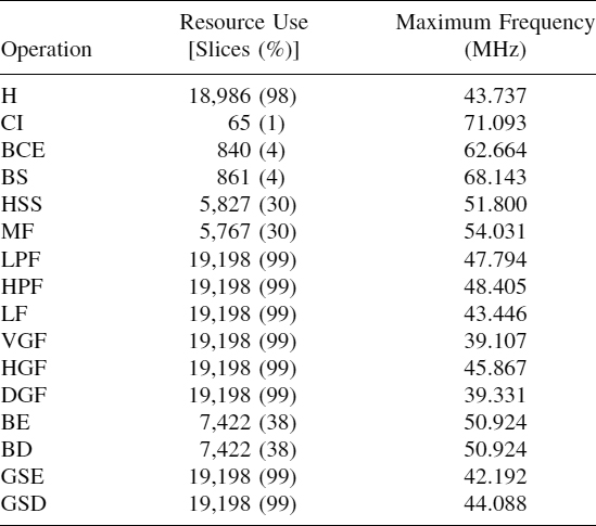
Table 18.1 presents the main characteristics of the various hardware circuits implemented: histogram (H), complement image (CI), binary contrast enhancement or thresholding (BCE), brightness slicing (BS), histogram sliding and stretching or brightness/contrast adjustment (HSS), median filter (MF), low-pass filter (LPF), high-pass filter (HPF), Laplacian filter (LF), vertical gradient filter (VGF), horizontal gradient filter (HGF), diagonal gradient filter (DGF), binary erosion (BE), binary dilation (BD), gray-scale erosion (GSE), and gray-scale dilation (GSD). More details about these operations are given in a book by Baxes [3]. As we can observe, operations working pixel by pixel use fewer FPGA resources (except in the histogram operation). This is due to the low computation cost of this operation type, since these operations only have to visit all the image pixels (or simply the image color table) and update the pixel values according to the values provided by a LUT.
In addition to the number of slices occupied, Table 18.1 includes the percentage of resources used (knowing that the Virtex-E 2000 FPGA has 19,200 slices). In all the operations we have striven to use the maximum number of FPGA resources performing replications, since this results in a shorter execution time (parallelism use). As for the operation frequency, all the operations admit at least 39 MHz and surpass 70 MHz in some cases. This high frequency allows us to obtain better performance.
18.4 ADVANCED DETAILS
Hardware modules are “programmed” by creating Handel-C models which are designed, simulated, and refined using the DK tool, and finally, synthesized using the Xilinx ISE platform. In each case, every module is implemented using the architecture that is best suited for real-time operation (high-speed execution) and for the FPGA device we use. We have performed very diverse optimizations in each module: use of techniques of parallelism such as replication and pipelining, optimization of the multipliers by means of adder trees in the convolution modules, reduction of the sorting and selection network in the median filter and the gray-scale morphological operations, search for high regularity, reutilization of common resources, and so on. Due to the great number of image-processing operations that we have implemented, in the following subsections we explain the implementation only for the most relevant image-processing operations. You can obtain more details in an article by Vega-Rodríguez et al. [4].
18.4.1 Image Convolution
Convolution is a very important operation in the field of image processing, and it has been used in a great number of applications [5,6]. Among these applications is its use for artificial vision highlights. The main challenge is that artificial vision systems are normally used in real-time applications. For this reason, the implementation of convolution by means of reconfigurable hardware is an important issue [7,8]. In fact, some proposals even use techniques such as simulated annealing and genetic programming to find the best implementation for convolution [9]:

Convolution is an operation of linear spatial filtering. For this operation, to apply the mask on a given position means to multiply each weight of the mask for the pixel of the image on which it is, and to add the resulting products. This sum is used as the value of the pixel for the output image. Therefore, the convolution of an image I with a square mask w of width n = 2k + 1 will generate an image O that could be defined by means of the weighted average of Figure 18.1 and Equation (18.1) [3]. The choice of the mask weights is what determines the action of spatial filtering to carry out, which can be a low-pass, high-pass, gradient, Laplacian, and so on, filter. On each convolution circuit we have carried out several important optimizations. As an example to explain these optimizations, we study which would be the resulting circuit to implement a low-pass filter. A popular mask for this filter is shown in Equation (18.2) [3]. In this case, the corresponding circuit could be implemented as shown in Figure 18.2 [3]. In this figure we observe the necessary nine dividers and the summing network (with eight adders). To avoid floating-point operations, we have normalized the mask coefficients to integer values. In this way the mask in Equation (18.2) is equivalent to the one shown in Equation (18.3), which can be implemented by means of five multiplication operations and only one division.

Figure 18.1 Example of a 3 × 3 convolution mask w.

Figure 18.2 Possible implementation of a low-pass filter.


First, we apply an optimization to the divider-multipliers. The optimization of the divider-multipliers in Figure 18.2 is carried out in two aspects. On the one hand, the implementation of a division whose divider is 16 can be performed by shifts (in this case, four positions on the right) instead of using a divider circuit. On the other hand, optimization of the multipliers is based on the use of adder trees. As an example, if we need the multiplication y = 51x, we can decompose it in y = 32x + 16x + 2x + x. Products that are a power of 2 can be implemented by means of shifts, or even more, by means of the use of connections with zeros (direct connections to ground).
Figure 18.3 illustrates the resulting circuit after this optimization (the number of bits in each adder and connection is indicated). In this figure, each product has been carried out by means of direct connections to ground. The final circuit “> >” symbolizes the right shift of 4 bits for dividing by 16. However, in our final architecture, not only the divider-multipliers have been optimized, but also the data paths, with the purpose of using fewer bits in each operation and connection, and therefore to improve system performance and reduce the necessary resources, as well as obtaining a more regular architecture. Figure 18.4 shows the resulting circuit for a low-pass filter after optimizing the data paths in the circuit of Figure 18.3. In this figure we also show the number of bits in each adder and connection so that we can compare this circuit with the one in Figure 18.3. In conclusion, we can see an important reduction in the number of bits, besides a more regular architecture (better parallelism exploitation, more common resources, etc). Evidently, both optimizations (divider-multipliers and data paths) will be more important when the convolution to be implemented is more complex.
Note that the fact of multiplying the result of the central column by 2 instead of using the initial coefficients [2,4,2] allows us to implement the three columns using the same hardware scheme (coefficients [1,2,1]), therefore simplifying the circuit design. Furthermore, this reduces the number of multiplications, because we multiply only the column result, not its three coefficients. Finally, it is necessary to divide the result obtained by 16, using shifts. Even more notably, the shift operation (the shift register) can be avoided by using appropriate connections. For example, in this case we have to discard the last 4 bits of the result.

Figure 18.3 Low-pass filter after applying divider-multiplier optimization.

Figure 18.4 Implementation of a low-pass filter after optimization.
Finally, using the statement par and function vectors of Celoxica Handel-C, we have replicated the resulting circuit (Figure 18.4 for a low-pass filter) in order to apply the corresponding convolution simultaneously on 148 pixel neighborhoods (the exact number of replications depends on the corresponding convolution, ranging from 138 to 148). In this way we take advantage of the inherent neighborhood parallelism, accelerating the operation 148 times.
18.4.2 Binary Morphology
Mathematical morphology [10] can be used to carry out very different tasks of image analysis, including elimination of noise, image enhancement, extraction of features, thinning/thickening, and shape recognition. In fact, it has been used with success in biomedical image analysis, robotics vision, industrial inspection, and other applications of artificial vision (several examples are explained in ref. 11). Morphology can be characterized as being computationally intensive, so it is difficult to implement it in real-time applications with general-purpose processors. This is a reason to study its FPGA implementation.
There are two forms of morphological processing: binary and gray scale [12]. For both forms, two basic operations exist: erosion and dilation. Erosion reduces the size of objects uniformly in relation to their background. Dilation, the dual operation, increases the size of objects uniformly. Morphological operators are implemented by means of nonlinear spatial filtering [3].
Binary morphological processing establishes the premises and methodology of image morphological processing. Binary morphological operators operate with binary images such as those created using thresholding. Therefore, we say that pixels possess logical values instead of brightness values. A black pixel is usually said to be in the 0-state and a white pixel is said to possess the 1-state. Here erosion and dilation combine the values of the pixels logically with a structuring element (or morphological mask). This structuring element is similar to the mask used in a convolution but has logical values instead of weighting values. Each logical value can have a 0- or 1-state. According to morphological mathematics, the binary erosion of an image I with regard to a structuring element w is expressed by the subtraction of Minkowski:
Similarly, the binary dilation of an image I with regard to a structuring element w is expressed as.
These mathematical expressions can be clarified by means of the use of morphological masks and the equation [3]

Assuming 3 × 3 structuring elements (as in Figure 18.1), in a binary morphological operation each pixel in the image and its eight neighbors are compared logically to the values of the structuring element. When the nine input pixels are identical to their respective mask values, the resulting pixel value is set to a predefined logical value 1 for erosion and 0 for dilation. If one or more input pixels differ from their respective mask values, the resulting value is set to the opposite state. Equation (18.6) presents the general equation for erosion and dilation, assuming an input image I and an output image O.
In the erosion case, the structuring element only has elements with a 1-state. For the dilation, the mask only possesses elements with a 0-state. Erosion and dilation are considered primary morphological operations, being the base of many other morphological operations. For example, the opening operation is simply erosion followed by dilation:
Similarly, the closing operation (opposite of opening) is defined like dilation followed by erosion:
Due to the great similarity between both operations, binary erosion and dilation, they have been designed jointly in one hardware module. These operations have been implemented as shown in Figure 18.5, where I(x + i, y + j) makes reference to each of the nine pixels covered by the 3 × 3 mask. As these operators are applied to binary images, each input pixel will be white (11111111 in binary) or black (00000000). To simplify, instead of using 8-bit pixels, in the implementation of these operators, 1-bit pixels are used. So in each input pixel, the most significant bit only is used. This bit will be 1 (white) or 0 (black). The use of only one bit for the pixels allows us to simplify the circuit, being able to use OR and AND gates.
Finally, the input Operation, also of 1 bit, indicates if an erosion (1) or a dilation (0) is being carried out. This input is used in a 2 : 1 multiplexer to obtain the correct output pixel O(x, y). Notice that for saving resources the output of the multiplexer has been wired eight times. Thus, an 8-bit bus is obtained and the use of more complex logic to generate the values 0 and 255 is avoided. It is important to emphasize that this implementation (Figure 18.5) is better than the direct implementation of Equation 18.6 (with nine comparators of 8 bits).

Figure 18.5 Implementation for binary erosion and dilation.
On the other hand, using the statement par and function vectors of Handel-C, we have replicated the circuit of Figure 18.5 in order to apply the corresponding operation simultaneously on 402 pixel neighborhoods, thereby accelerating the operation 402 times (use of inherent parallelism).
18.4.3 Gray-Scale Morphology
Gray-scale morphological operators are a continuation of binary techniques, allowing direct processing of gray-scale images. Mathematically, the erosion (E) and dilation (D) operations are


respectively, where F and G are the index domains of I and w, respectively. I(x, y) represents the value of the pixel at image I in the position (x, y). w(i, j) indicates the value of the structuring element w in the position (i, j). These expressions can be clarified by means of the use of morphological masks and [3]

The central mask value and its eight neighbors are added to the corresponding input pixels. For the erosion case, the structuring element is formed by values that range from −255 to 0, while for the dilation the values range from 0 to 255. The output value is determined as the minimum/maximum (minimum for the erosion and maximum for the dilation) value of these nine sums.
As in binary morphology, the gray-scale erosion and dilation is the base of many other morphological operations: for example, opening and closing, which are defined like their binary equivalents. Gray-scale erosion and dilation have been designed by means of two different hardware modules. Although two hardware modules have been developed, these possess a similar scheme of operation. We explain this scheme now, and later we detail the differences between the two operations. Both erosion and dilation follow the general scheme shown in Figure 18.6, where I(x + i, y + j) makes reference to each of the nine pixels (of 8 bits) covered by the 3 × 3 mask. The structuring element has values between 0 and 255 (A, B, …, I) to subtract (erosion) or to add (dilation) with the associate pixel.

Figure 18.6 Implementation of gray-scale dilation and erosion.
In the case of erosion, Figure 18.7 illustrates the internal scheme for each of the circuits Prepare and M. For the circuit Prepare, the corresponding mask element W n is subtracted from the pixel I(x + i, y + j) using an 8-bit unsigned binary subtracter. Then the multiplexer allows us to control if the resulting value is negative, replacing it by 0. The outputs of the nine circuits Prepare are used inside a partial-sorting network that allows us to select the output that possesses the minimum value. For that, the sorting and selection network consists of eight nodes M.

Figure 18.7 Circuits Prepare and M for the gray-scale erosion operation.

Figure 18.8 Circuits Prepare and M for the gray-scale dilation operation.
In the case of dilation, Figure 18.8 presents the internal scheme for the circuits Prepare and M. The corresponding mask element W n is added to the pixel I(x + i, y + j) using an 8-bit unsigned adder, and the multiplexer allows us to control if the resulting value is higher than 255. Afterward, the outputs of the nine circuits Prepare are used inside a partial sorting network that makes it possible to select the output that has the maximum value.
Finally, it is important to indicate that for these operations (gray-scale erosion and dilation) we have been able to replicate the corresponding circuit 148 times, therefore accelerating the operation 148 times (application of the operation simultaneously on 148 pixel neighborhoods).
18.5 EXPERIMENTAL ANALYSIS: SOFTWARE VERSUS FPGA
Table 18.2 presents several comparisons between the software and hardware (FPGA) versions of the different image-processing operations. The software versions are executed on a 1.7-GHz Pentium-4 with 768M bytes of RAM, and the hardware versions, on a Virtex-E 2000 FPGA. The software versions are written in C++ and compiled with the appropriate optimizations. All the results refer to images with 256 gray levels and they are expressed in seconds. These times also include the communication time, and they are the average response times after 10 executions of each experiment. In order not to influence the results, all the measurements in Table 18.2 have been made with the same workload in the server.
As we can observe in Table 18.2, FPGA implementation is always better than software implementation. Furthermore, the larger the image, the higher the benefits obtained by hardware (FPGA) execution, since a larger image implies greater use of the hardware computation capability, that is, greater exploitation of the inherent parallelism in image-processing operations.
The hardware implementation of all the pixel-by-pixel operations (except the histogram) always have the same execution time, because they take advantage of the existence of the image color table (all the 8-bit images have this color table), performing their operation on the color table, and their performance is therefore independent of image size.
TABLE 18.2 Comparisons Between the Software (Pentium) and Hardware (FPGA) Versions

On the one hand, we can notice clearly that the result obtained by median filter is not as good as for other operations. On the other hand, binary erosion and dilation demonstrate great speedup (more than 149 times faster).
18.6 CONCLUSIONS
Image processing has always been a focus of interest for programmable logic developers. However, the use of FPGAs in image processing is still a research area, and although many hardware developments exist, so far no complete system has been proven competitive enough to establish a significant commercial presence.
In this chapter we have described the FPGA-based implementation and optimization of many different image-processing algorithms. In fact, 16 hardware implementations have been studied, all clearly improving the performance obtained by software (some operations are more than 139 times faster). These results are possible because we have applied many different optimizations to our FPGA-based implementations. In particular, our implementations use several parallelism techniques, include other operation-specific optimizations, and have high operational frequencies. Thanks to this, very good execution times are obtained.
Acknowledgments
This work has been supported in part by the Spanish government under grant TIC2002-04498-C05-01 (the TRACER project) and grant TIN2005-08818-C04-03 (the OPLINK project).
REFERENCES
1. M. A. Vega-Rodríguez, J. M. Sánchez-Pérez, and J. A. Gómez-Pulido. Guest editors' introduction—special issue on FPGAs: applications and designs. Microprocessors and Microsystems, 28(5–6):193–196, 2004.
2. M. A. Vega-Rodríguez, J. M. Sánchez-Pérez, and J. A. Gómez-Pulido. Recent advances in computer vision and image processing using reconfigurable hardware. Microprocessors and Microsystems, 29(8–9):359–362, 2005.
3. G. Baxes. Digital Image Processing: Principles and Applications. Wiley, New York, 1994.
4. M. A. Vega-Rodríguez, A. Gómez-Iglesias, J. A. Gómez-Pulido, and J. M. Sanchez-Perez. Reconfigurable computing system for image processing via the Internet. Microprocessors and Microsystems, 31(8):498–515, 2007.
5. R. Haralick and L. Shapiro. Computer and Robot Vision. Addison-Wesley, Reading, MA, 1992.
6. E. Dougherty and P. Laplante. Introduction to Real-Time Imaging. SPIE Press, Bellingham, WA, 1995.
7. E. Jamro and K. Wiatr. FPGA implementation of addition as a part of the convolution. In Proceedings of the EuroMicro Symposium on Digital System Design, Warsaw, Poland. IEEE Computer Society Press, Los Alamitos, CA, 2001, pp. 458–465.
8. S. Perri, M. Lanuzza, P. Corsonello, and G. Cocorullo. SIMD 2-D convolver for fast FPGA-based image and video processors. In Proceedings of the International Conference on Military and Aerospace Programmable Logic Devices, Washington, DC, 2003.
9. E. Jamro and K. Wiatr. Genetic programming in FPGA implementation of addition as a part of the convolution. In Proceedings of the EuroMicro Symposium on Digital System Design, Warsaw, Poland. IEEE Computer Society Press, Los Alamitos, CA, 2001, pp. 466–473.
10. R. Haralick, S. Sternberg, and X. Zhuang. Image analysis using mathematical morphology. IEEE Transactions on Pattern Analysis and Machine Intelligence, 9(4):532–550, 1987.
11. H. Joo and R. Haralick. Understanding the Application of Mathematical Morphology to Machine Vision. In Proceedings of the IEEE International Symposium on Circuits and Systems, Portland, OR, vol. 2, 1989, pp. 977–982.
12. C. Giardina and E. Dougherty. Morphological Methods in Image and Signal Processing. Prentice Hall, Upper Saddle River, NJ, 1998.
Optimization Techniques for Solving Complex Problems, Edited by Enrique Alba, Christian Blum, Pedro Isasi, Coromoto León, and Juan Antonio Gómez
Copyright © 2009 John Wiley & Sons, Inc.