
CHAPTER 16
A DDS VFO
There was a time when a transmitter consisted of a single vacuum tube operating as a keyed oscillator. Well, you can imagine what that sounds like on the air! “CW” was not called “chirpy warble” for nothing. Crystal oscillators improved on the stability of the early transmitters a great deal, but with a crystal, you are, for the most part, stuck on one frequency, which meant you needed a lot of crystals if you wanted to move around the bands. Along comes the Variable Frequency Oscillator or “VFO” and suddenly we were free to move about the bands. But, VFOs still tended to drift a lot during warm-up and were sensitive to many variables, not the least of which might be the operator’s body capacitance.
Today, it seems, we can’t get by without having a digital frequency readout down to the millihertz and stability that rivals the national frequency standards at NIST. Still, we do strive to know accurately our operating frequency and it is not all that hard today, with some readily accessible technologies. Enter, the Direct Digital Synthesis VFO or DDS VFO.
Synthesized frequency generators have been around for some time. Most modern amateur radios use one form of synthesizer or another. One common type is the Phase-Locked-Loop, or PLL, synthesizer. We have already played with a PLL circuit in the Morse code decoder in Chapter 8. Shown in Figure 16-1, a PLL synthesizer uses a Voltage Controlled Oscillator, or VCO, to generate the output frequency. A small portion of the output is fed back through a divider and then compared to a stable reference oscillator, generally a crystal oscillator. The difference between the reference and the divided down VCO output is then negatively fed back to the VCO so that any variation in the output frequency causes a small error voltage to be generated, pulling the VCO back in the opposite direction to the original variation. The result is a stable output frequency. Changing the divider value allows the VCO to move to other frequencies.
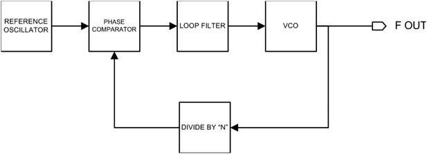
FIGURE 16-1 The Phase-Locked-Loop synthesizer.
While PLL synthesizers are available, we chose not to use one for this project. We use a different type of synthesizer, the Direct Digital Synthesizer (DDS), for this Arduino Project.
Direct Digital Synthesis
Direct Digital Synthesis or DDS is a fancy name for a type of frequency source that digitally generates the desired frequency. As you can see in Figure 16-2, the key elements of the DDS are the Numerically Controlled Oscillator (NCO) and the Digital to Analog Converter (DAC). The NCO produces a numerical representation of the output of signal, generally a sine wave, that is then turned into an analog output by the DAC. The NCO is controlled by the “Frequency Control Register,” a fancy name for a register that contains the digital value of the desired output frequency. The output is “cleaned up” with a low pass filter, removing any harmonic content. The entire device uses a stable reference clock to maintain accuracy. Of course, this architecture lends itself to being controlled by a digital processor such as an Arduino. Arduinos can be very good at stuffing a digital value into a register on some external device (as we have done in projects such as the Station Timer/Real Time Clock in Chapter 4).
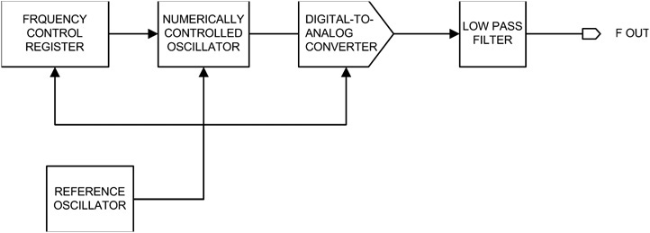
FIGURE 16-2 The direct digital synthesizer.
The DDS VFO Project
Because of the complexity of the software, this project requires an ATmega328 or higher μC. The software requirements force this choice not because of the Flash memory limitations of the smaller chips, but rather because of the SRAM limitations. As you recall, SRAM is used for temporary storage for variables, plus the compiler copies string literals into SRAM unless you use the F() macro to prevent it. Finally, the software uses interrupt service routines (ISR) to react to signals sent from a rotary encoder. Because the 328 family of μC chips only has two interrupt pins (i.e., pins 2 and 3) for external interrupts, the LCD display is managed somewhat differently, too.
Our DDS VFO uses an Analog Devices AD9850 DDS chip. The AD9850 is a DDS synthesizer capable of generating a clean sine wave up to 62.5 MHz (spurious emissions at least 43 dB below the output frequency), operates on 5 VDC, and is housed in a 28-pin SSOP surface mount package. Now, before you get all excited about having to deal with a surface mount part again, even though we showed you the sure-fire method of soldering SMD parts, we use a preassembled breakout module that uses the AD9850. All the “dirty work” is already done! The module consists of the AD9850 DDS chip, a 125 MHz reference oscillator and the output low pass filter. The whole thing is built on a small circuit board that can be mounted on a prototype shield with header pins and sockets (so that the module can be removed) or soldered directly to the proto shield with header pins alone. A sampling of eBay DDS modules using the AD9850 is shown in Figure 16-3. The DDS module we used is the one to the right in Figure 16-3. As shown in the same photograph, the underside of the module has the pinouts clearly marked. These modules are available on eBay for under $5!
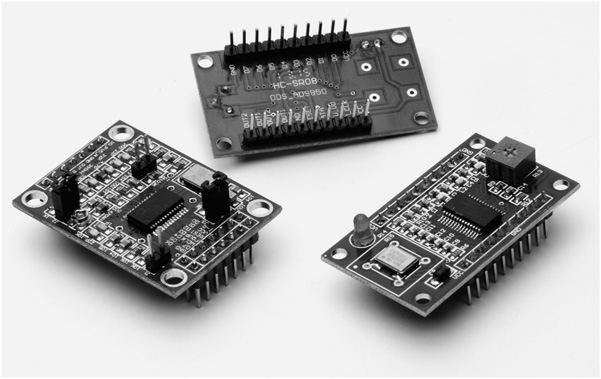
FIGURE 16-3 DDS breakout module.
As we stated earlier, a DDS module lends itself well to digital control. We take advantage of that by creating a VFO that employs many features that are provided through software. The completed DDS VFO is shown in Figure 16-4. The project comprises a DDS shield, the DDS VFO software, and a control panel board to operate the VFO. The control panel is the control panel board we used in Chapter 13 for the rotator controller. Here is a list of features we include in this design:
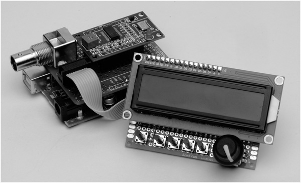
FIGURE 16-4 The completed DDS VFO with BNC output.
• Frequency coverage of HF ham bands (160 through 10 meters)
• Frequency readout to 10 Hz
• Marked band edges
• One memory per amateur band
DDS VFO Circuit Description
The schematic diagram for the DDS VFO shield is shown in Figure 16-5. As with the Rotator Controller in Chapter 13, we use the I2C bus interface (analog pins 4 and 5) and the external interrupt pins (digital pins 2 and 3), which are “passed through” the shield. Device A1 is the DDS module. The module has four inputs and one output that are used. Other than VCC and ground, all remaining pins are not used. Table 16-1 lists the parts needed for the DDS VFO shield.
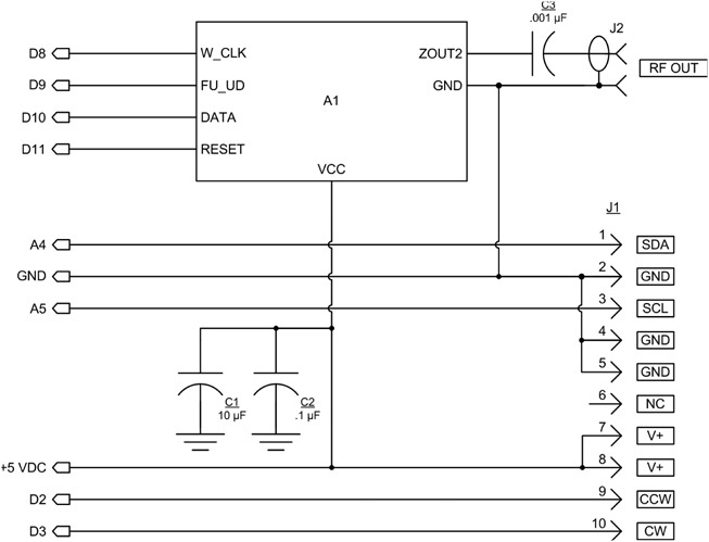
FIGURE 16-5 DDS VFO shield schematic.
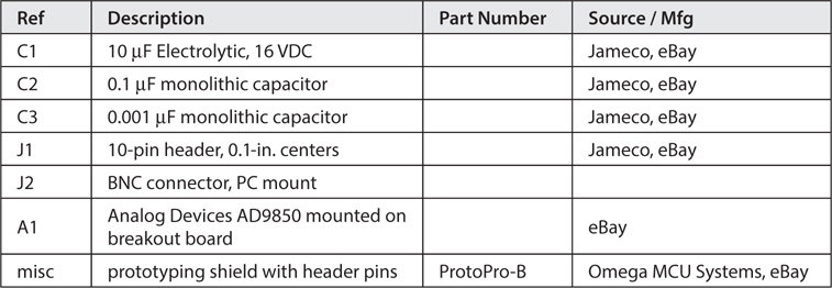
TABLE 16-1 DDS VFO Shield Parts List
The Analog Devices AD9850 Breakout Module
The AD9850 breakout module that we obtained from eBay is a small circuit board with two 10-pin headers already installed as shown in Figure 16-3.
Constructing the DDS VFO Shield
We again chose to use the ProtoPro-B prototyping shield for assembling the DDS VFO. Header sockets are used to connect to the DDS breakout module and two 5-pin headers are used to provide a connection to the control panel board. The layout shown is for the DDS breakout module that we used. There are several different varieties available, so make sure that if yours is a different type, check the pinouts by the signal name as they are probably different.
We built several versions of the DDS VFO shield. One version uses a BNC connector for the output (see Figure 16-4) while another uses a 2-pin 90-degree header (J2) as shown by the layout in Figure 16-6. The connector you use is a matter of personal choice and depends upon how you intend to use the project. For the version with the 2-pin header, we assembled a short jumper cable that terminates with a BNC connector.
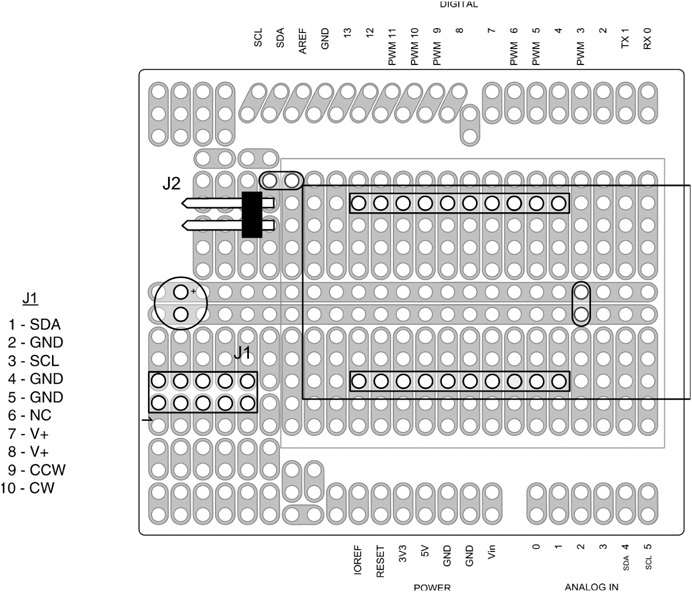
FIGURE 16-6 Parts layout for the DDS VFO shield.
The wiring of the shield is shown in Figure 16-7. We used our standard wiring method of using bare tinned wire and Teflon tubing. Using a drill, we had to slightly enlarge the two holes for the mounting pins to go through the proto board in order to use the PC-mount BNC connector. Figure 16-8 is a photograph of the completed DDS VFO shield showing the BNC connector we used.
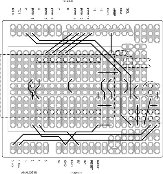
FIGURE 16-7 Wiring diagram for the DDS VFO shield.
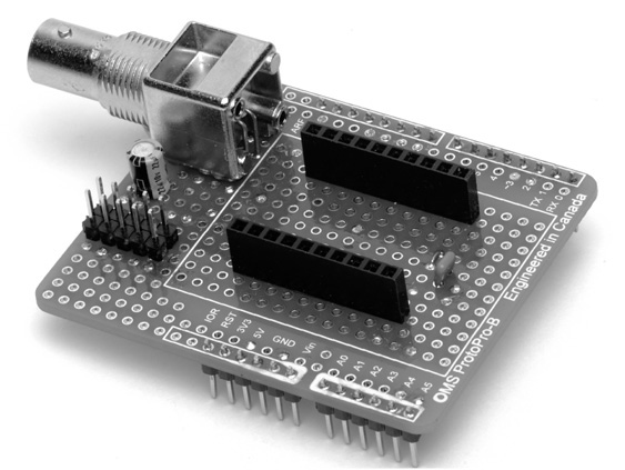
FIGURE 16-8 The completed DDS VFO shield.
The wiring side of the completed DDS VFO shield is shown in Figure 16-9.
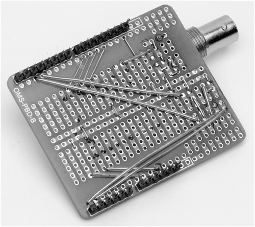
FIGURE 16-9 Wiring side of the completed DDS VFO shield.
Adding an Output Buffer Amplifier for the DDS VFO
For some applications, the output level from the DDS module alone may be too low (about 500 mV). Such is the case if you drive vacuum tube gear, which typically needs a 5 to 7 V signal level. We added a simple buffer/gain stage to the output to kick the voltage level up a bit. We show two additional drawings for the buffered version of the DDS VFO. Figure 16-10 is the schematic for the shield and Figure 16-11 is the wiring diagram. The wiring diagram also shows our version that uses the PC-mount BNC connector. The additional parts needed for the output buffer are listed in Table 16-2.

FIGURE 16-10 DDS VFO shield schematic with added output buffer.
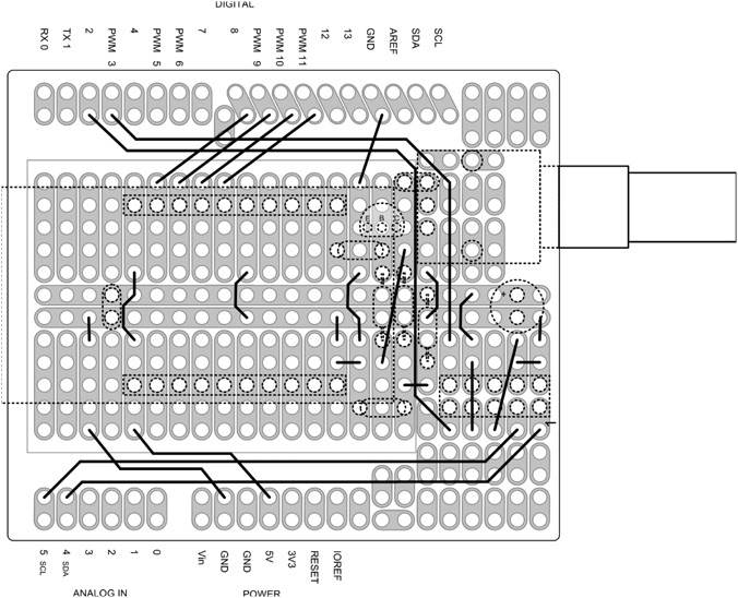
FIGURE 16-11 Wiring diagram for DDS VFO shield with buffered output.
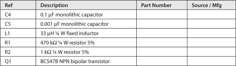
TABLE 16-2 Additional Parts Needed for the DDS VFO Buffer
The Front Panel and Interconnection
We use the rotator controller control panel board from Chapter 13 with no changes. Refer back to Chapter 13 for the details on constructing the control panel board. We made a short jumper cable to connect the control panel to the DDS VFO shield using ribbon cable and FC-10P connectors just as we did in Chapter 13. If you are mounting the DDS VFO in its own enclosure, make sure that you make the cable long enough.
You are now ready to connect it all together and begin testing. First, as always, make sure that you double-check all of your wiring. Remember, you can use a multimeter to measure the continuity between the points on the schematic. If you don’t have a multimeter, then perform a careful visual inspection. Once you are satisfied with your work, you can connect the pieces together and start loading the software.
However, before we jump into a discussion of the software, it is helpful to first understand the functionality of each of the controls depicted in Figure 16-4. Understanding what those controls do makes understanding the software that much easier.
DDS VFO Functional Description
The user interacts with the VFO via a program sketch (VFOControlProgram.ino) that manages the hardware. We refer to this program as the User Interface Program (UIP). There are five pushbutton switches (SW1 through SW5) that control most of the functionality of the VFO. A sixth switch (SW6), also a pushbutton switch, is part of the rotary encoder. An explanation of what each of these switches do provides a good description of the functionality of the VFO. We discuss these switches in a left-to-right manner, which is the order in which they appear on the control panel.
Overview
When the DDS VFO is initially turned on, the frequency stored when you last used the DDS VFO is read from EEPROM memory. That frequency is then displayed on line 1 of the LCD display. Line 2 of the display shows the ham band associated with the displayed frequency. Figure 16-12 shows what the display might look like when you power it up. In Figure 16-4, you can see the DDS shield with the breakout module that holds the AD9850 chip piggybacked onto an Arduino Duemilanove. The ribbon cable connects the DDS VFO shield to the control panel board, with the LCD, pushbutton switches, and rotary encoder. The display in Figure 16-12 shows the DDS VFO powered up, displaying the lower band edge for 80 meters.
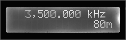
FIGURE 16-12 Initial VFO state on power up.
EEPROM Memory Map
The ATmega328 μC family has 1024 bytes of EEPROM memory available for use. The software that controls the UIP views the EEPROM memory space as a sequence of 4-byte chunks, which we call a record. A record in our EEPROM memory space is defined as one unsigned long. The memory map for the EEPROM is shown in Figure 16-13. Table 16-1 presents the interpretation for each of the records shown in Figure 16-13. Because each record is a 4-byte memory space, record 0 is actually EEPROM address space 0-3. Record 1 occupies EEPROM addresses 4-7 and so on. While you could write all of the EEPROM memory addresses using the features of the VFO, we have written a short program (discussed later in this chapter) that writes the default frequencies mentioned in Table 16-3.
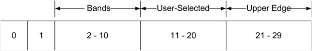
FIGURE 16-13 Record mapping for EEPROM memory.
TABLE 16-3 EEPROM Memory Map for Records
As mentioned earlier, on power-up, record 0 is fetched from EEPROM and displayed on the first line of the LCD display. The second line of the LCD display is used to display the band in which the frequency falls (e.g., “80m”). The output frequency of the VFO matches the frequency displayed on line 1 of the LCD display.
What happens next depends upon which switch you push. We’ll assume you push them in left-to-right order (SW1 through SW5). The switch placement is illustrated in Figure 16-14.
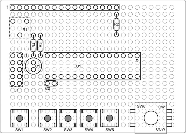
FIGURE 16-14 Component placement on control panel board.
SW1, the User Frequency Selection Switch (UFSS)
We named switch SW1 User Frequency Selection Switch because it is used to store and review user-selected frequencies. (It is the left-most pushbutton switch seen near the bottom of Figure 16-14.) In terms of the memory map shown in Figure 16-13, you are working with EEPROM records 11 through 20.
SW1 REVIEW Mode
When you press SW1, line 2 displays the word REVIEW on the LCD display to indicate you are in the REVIEW mode. The first time you run the UIP program, and assuming you have first run the VFO Initialization Program (discussed later), you should see the 160 meter QRP default frequency, 1818 kHz. This frequency is the first EEPROM record (record 11) in the user-selected memory space shown in Figure 16-13. You can now rotate the rotary encoder control (SW6 in Figure 16-14) to scroll through the 10 user-selected frequencies. As mentioned earlier, the first time through you are presented with the default (North America) QRP CW frequencies for each band. The tenth address (i.e., record 20) is simply the upper-edge frequency for 10 meters. If you rotate past the last user-selected frequency, the display “wraps around” to the first frequency (i.e., moves from record 20 back to record 11).
SW1 STORE Mode
For example, suppose you want to change the upper-edge frequency for 10 meters (record 20) from 29,700,000 Hz to 29,699,990 Hz. To do that, first scroll to the frequency to change (i.e., 29,700,000 Hz) by rotating the encoder control while in the REVIEW mode. Once you see the target frequency displayed (i.e., 29,700.000 kHz), touch the UFSS switch, SW1, a second time. You immediately see the second line display change from REVIEW mode to STORE mode. This means you are going to store a new frequency in record 20 and replace the 29,700,000 Hz frequency with a new frequency.
Rotate the encoder control counter clockwise one “click,” or one position. The frequency display should now show 29,699.990 kHz. In other words, once you see the STORE mode is active, rotating the encoder control alters the frequency shown on line 1 of the LCD display. As you would expect, rotating clockwise raises the displayed frequency and rotating the control counterclockwise lowers the displayed frequency. As you can see, the default frequency step is set to 10 Hz. (The default step is set with switches SW4 and SW5, discussed later. For now, we’ll just use the default 10 Hz step.)
Storing a New Frequency
To store the new displayed frequency in record 20 of the EEPROM memory space, push the encoder control shaft. The new frequency is then stored for you. The program immediately resets itself to the BANDUP mode. We force the code to limit itself to a single write using the STORE mode just to make sure you don’t overwrite some other frequency. Also recall that EEPROM has a finite number of write/erase cycles (about 100,000) before it can become unreliable, and we don’t want to waste those cycles. While that may sound like a lot of cycles, don’t forget that if you are just cruising around the band and the frequency has changed in the past 10 seconds, that new frequency is written to EEPROM.
If you press any other switch before pressing the encoder switch, SW6, the STORE mode is canceled.
SW2, the Band-Up Switch (BUS)
The Band-Up Switch is used to increase the current frequency from the current band to the next higher frequency band. Therefore, if you are currently displaying a frequency of 3.501 MHz (80 meters) and you press the BUS, you advance frequency to 7.0 MHz (40 meters). Each press of BUS advances to the low edge of the next higher band. There is nothing to prevent you from advancing the frequency to the next band by rotating the encode control a bazillion times. It’s just that the BUS gives you a faster way to move to the next highest band.
The supported bands are: 160, 80, 40, 30, 20, 17, 15, 12, and 10 meters. Once you reach the band you are interested in, you can rotate the encoder control to raise or lower the displayed frequency. Frequencies are always displayed on the first line of the LCD display, while “control information” appears on the second display line. As you rotate the encoder shaft, each “click” of the encoder control increases/decreases the frequency by an amount controlled by the STEP function (discussed in a few moments). If you advance the BUS past the 10 meter frequency, the displayed frequency wraps around to the lowest frequency (i.e., 1800 kHz or 160 meters).
Out-of-Band Condition
Suppose you have the BUS so that the VFO is displaying the lower edge of the 40 meter band (i.e., 7.000 MHz). If you have the STEP to (the default) 10 Hz and turn the encoder control counterclockwise, you display a frequency of 6,999.990 kHz, which is outside of the range of legal operation for most hams. Because the frequency lies outside of the ham bands, and asterisk (*) appears in the first column of the first line on the LCD display. This indicates that the displayed frequency lies outside of the ham band shown on the second line.
If the (illegal) state of the VFO is that shown in Figure 16-15 and you press the BUS again, the display would show 10,100 kHz, which is the lower edge of the 30 meter band. Because this edge is within the band limits, the asterisk would no longer appear on the LCD display.
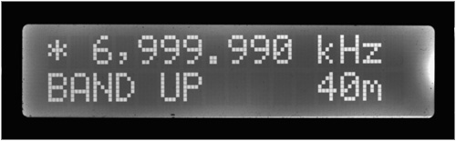
FIGURE 16-15 Frequency display with out-of-band condition.
SW3, the Band-Down Switch (BDS)
The BDS is used to decrease the current frequency to the next lowest band edge frequency. That is, BDS is a mirror opposite of the BUS switch. You can interleave the BDS and BUS switches to move quickly throughout the VFO’s amateur band spectrum. Again, you could rotate the encoder control counter clockwise and (eventually) get to the next lowest band edge. However, the BDS provides a much faster way to move to the next lower band edge.
SW4, Plus Step Switch (PSS)
We mentioned earlier that rotating the encoder control changes the displayed frequency plus or minus 10 Hz, depending upon which direction you rotate the control. The PSS can be used to alter the default frequency step amount. The allowable frequency steps are:
10 Hz 20 Hz 100 Hz 0.5 kHz 1 kHz 2.5 kHz 5 kHz 10 kHz 100 kHz 1 MHz
Because the default step is 10 Hz, if you press the PSS, the display changes to 20 Hz and the +STEP mode is displayed. This can be seen in Figure 16-16. Now each “click” of the encoder control changes the frequency by 20 Hz. This step can be used to increase or decrease the displayed frequency.
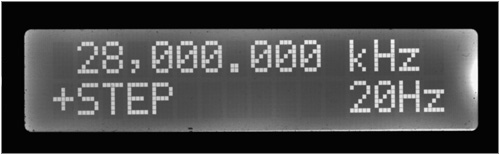
FIGURE 16-16 Using PSS.
If the LCD display shows the PSS at 1 MHz and you press it one more time, the display changes to 10 Hz. That is, the PSS wraps around to the lowest step.
SW5, Minus Step Switch (MSS)
As you might expect, the MSS does the opposite of the PSS. If the LCD displays 5 kHz and the –STEP mode, pressing the MSS changes the step to 2.5 kHz. If you press the MSS while the 10 Hz step is displayed, the step wraps around to 1 MHz for the frequency increment. You can interleave PSS and MSS to move about in the step ranges very quickly.
Once you have set the STEP to your desired value, press the BUS or BDS to go back to the tuning mode. If you don’t press one of these two switches, you’ll just end up cycling through the various steps.
SW6, the Encoder Control
The encoder control is actually two parts: 1) a shaft that can be rotated in either direction to change the displayed frequency, or 2) to push the shaft to activate the switch component of the control. The switch component only has meaning when SW1 is in the STORE mode, as explained earlier. Therefore, the primary function of the encoder control is to alter the displayed frequency.
You now know how to use all of the controls on the DDS VFO. The software behind those controls is explained in the next sections.
The DDS VFO Software
One of the features of the DDS VFO is the ability for you to store your own favorite frequencies as part of the DDS VFO. You might, for example, have a frequency for a net that you check into each week, or some other frequency you use to keep in touch with another ham. All of us probably have favorite bands we like to use, and perhaps specific frequencies within those bands. As shown in Figure 16-13, you can store up to 10 such frequencies. Because you want these frequencies to persist even when you turn the DDS VFO off, we write those frequencies to EEPROM memory. Because EEPROM is non-volatile memory, those frequencies persist even after power is removed.
You might ask: Flash memory is also nonvolatile, so why not store your 10 favorite frequencies in Flash memory? True, that is possible, but what if you want to change one of those frequencies? Your only alternative is to load the DDS VFO source code, edit the frequency list, recompile, and upload the new program to the Arduino. So, yes, you could use Flash memory to hold the user-defined frequency list, but changing that list is not very convenient. It also assumes the user you lent your new DDS VFO to is also a programmer. Maybe … maybe not. It just seems like a better design decision to change user-defined frequencies in EEPROM as the program is running rather than having to edit, recompile, and upload a new version of the program. However, when you have finished building your version of the DDS VFO, you can code your favorite frequencies into the source code so you don’t have to edit them at runtime. This saves you from needing to use the REVIEW/STORE features the first time you run the DDS VFO.
EEPROM Initialization Program
LISTING 16-1 presents a short program that initializes EEPROM memory to a set of frequencies. You should load this initialize EEPROM program into your Arduino and run it before you run the VFO program.
There are three EEPROM record blocks that the program initializes:
1. The 10 user-defined frequencies.
2. The nine frequencies that represent the lower band edges for the frequencies covered by the VFO.
3. The nine frequencies that represent the upper band edges for the frequencies covered by the VFO.
Unless the FCC changes things, you should not edit the last two EEPROM blocks. You should only edit the first, user-defined, EEPROM memory block. As the code is currently written in Listing 16-1, the 10 user-defined frequencies are the common North America QRP frequencies for each band. As we mentioned earlier, since there are only nine bands, we set the 10th address to the upper band edge for 10 meters. The reason for selecting this frequency for the 10th position is … we don’t have a reason. Make it anything you wish, as the user-defined frequencies are not integral to the needs of the rest of the program. If you have other frequencies you’d prefer to have in the list, you can edit the qrp[] array to reflect those new frequencies. Just make sure you end up with 10 frequencies in the qrp[] array … no more, no less.
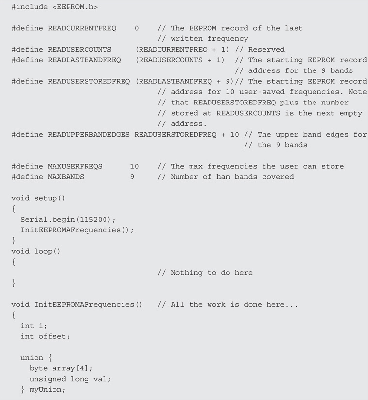

LISTING 16-1 Initialize EEPROM data.
If you have less than 10 “favorite” frequencies, it’s okay to leave them blank. However, if you do initialize less than 10 frequencies in this program and your EEPROM has never been set before, you may see 4,294,967,296 pop up as a displayed frequency. The reason is because unwritten EEPROM bytes are usually set to 0xFF, which, when viewed as a 4-byte unsigned value, is 4,294,967,296. If you make an error and attempt to write 11 user-defined frequencies, the code creates a small black hole in your EEPROM and the VFO disappears under its own weight. Well … not really, but you will likely blow away one of the upper band edge values. If you do that, edit the extra frequency out of the user-defined list and rerun this initialization program.
You should not edit the other two array contents, lowBandEdge[] and hiBandEdge[] unless the FCC changes the band edges. The content of these arrays is used by the DDS VFO in different ways, and changing them would likely break some of the functionality of the DDS VFO. You should view these two arrays as etched in stone.
Wait a minute!
If the lowBandEdge[] and hiBandEdge[] arrays are fixed, why not simply hardcode them into the program as static or global arrays? Believe us, life would be much simpler if we could. However, because we wanted you to be able to run the VFO using a 328-based Arduino, we only have 2K of SRAM available for variables. Keep in mind that the stack and the heap use SRAM, which means the amount of unused SRAM ebbs and flows as the program runs. When we tried to run the program with the lowBandEdge[] and hiBandEdge[] arrays as part of the program space, the program did a lot of ebbing and no flowing. At one part of the program, we simply ran out of SRAM memory and the program died an inglorious death. Our only recourse was to place the arrays in EEPROM memory space.
The program doesn’t do all that much. Basically, the program takes the contents of the three arrays, writes them to EEPROM memory, and displays a few messages on the Serial object so you know it ran. Because there’s nothing to repeat, the loop() function is empty. All of the work takes place in setup().
There is one aspect of the program that is a little unusual. The code fragment:
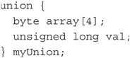
uses the C keyword union; a keyword you don’t see that often in C programs. Perhaps the easiest way to think of a union is as though it is a shapeless chunk of memory that you’ve set aside to hold some piece of data. What makes a union unique is that you don’t know exactly what it holds at any given moment. In our program, all we are saying is that we have defined the union so that it is large enough to hold either a 4-byte array or a single unsigned long data type. Functionally, a union is a buffer where we can place different types of data. It’s up to the programmer to keep track of what’s actually in the buffer.
Given that we have defined myUnion to hold either a 4-byte array or an unsigned long, both of which require four bytes of memory, myUnion ends up occupying 4 bytes of memory. If we had added an array of 10 integers (i.e., myInts[10]), myUnion would now require 20 bytes of memory because each int requires two bytes. The data definition would now look like:
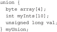
In that case, myUnion now defines a memory space that would occupy 20 bytes of memory. The rule is: A union always requires an amount of memory equal to the largest data item defined in the union.
So, what does a union bring to the table? Well, first of all, we could have defined all three members of the union separately as:
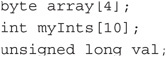
and used the data accordingly. However, doing so means we are now using 28 bytes of memory rather than just 20. A byte here … a byte there, pretty soon it adds up. So, one advantage is that a union saves us a little memory. That’s the good news.
The bad news is that when using a union, it can only hold a value for one of those three members at any given moment and you need to keep track of what’s actually living inside the union when you go to use it. You use the dot operator when assigning or retrieving a value from a union:
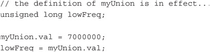
We talked about the dot operator before in the integration chapter (Chapter 10). Note the dot operator appears between the union name (myUnion) and the union member we wish to use (val). You can verbalize the dot operator in the example above as: “Go to the union memory address space named myUnion, fetch unsigned long bytes of that memory space (4 bytes), and subsequently reference those four bytes as the val member of that union.” The dot operator is like a key to get inside a black box. In Object Oriented Programming jargon, the dot operator is the key that opens a black box object named myUnion and, once inside the black box, allows you access to the object member named val.
Note how we use the union in Listing 16-1. We stuff each frequency element of the qrp[], lowBandEdge[], and hiBandEdge[] arrays into the union as an unsigned long, but extract that data from the union as though it is a 4-byte array of bytes. We do this because the EEPROM read() and write() functions in the EEPROM library can only read and write data one byte at a time. For example, suppose you knew that an unsigned long was stored at EEPROM memory address 10. That unsigned long occupies EEPROM memory addresses 10, 11, 12, and 13. Now, if we want to retrieve that unsigned long using the statement:
unsigned long frequency = EEPROM.read(10);
the program goes to the EEPROM memory address 10, reads the byte stored there, and assigns it into frequency. The problem is that read() only returned one byte—the byte stored at EEPROM address 10. The variable frequency now contains ¼ of an unsigned long! By using the union, we can stuff the frequencies into the myUnion.val member as an unsigned long, but then write them out to EEPROM memory as four separate bytes. We don’t have to know if an unsigned long is stored with its bytes in ascending or descending order … they are just bytes to us. Likewise, we can read the unsigned long from EEPROM memory as 4 separate read() function calls, and then extract the unsigned long from the union via the val member.
When you finish running the program in Listing 16-1, the EEPROM memory space is ready for use. We can now move on to the program that controls the KP VFO.
The KP VFO Software (VFOControlProgram.ino)
Unlike previous programs, we are not going to list the entire KP VFO software program. It’s simply too long and you can download it at a McGraw-Hill web site (www.mhprofessional.com/arduinohamradio). Instead, we are going to discuss those sections that may be of interest to you should you want to change the way the VFO functions from a user interface point of view.
The code associated with the rotary encoder is largely taken from Richard Visokey’s work with the AD9850 DDS chip. You can download his rotary library at
http://www.ad7c.com/projects/ad9850-dds-vfo/.
The program also uses the Adafruit port expander code, which can be downloaded from
https://github.com/adafruit/Adafruit-MCP23017-Arduino-Library/.
You should be pretty well versed in how to download and add these libraries to the Arduino IDE so we won’t repeat those instructions here. After you have downloaded and installed the libraries called by the various #include directives, load the VFOControlProgram.ino sketch. The VFOControlProgram sketch also has two additional source code files (W6DQ_DDS_VFO.h and W6DQ_DDS_VFO.cpp). These files are necessary to create additional objects required by the program.
We should state at the outset that we are not totally happy with the structure of this program. Indeed, we desperately wanted to add a new class source code file to handle all of the user interface elements of the program. However, we also want the VFO to fit in the memory space allocated to the 328 type of Arduino boards, which is limited to 2K of SRAM. Our program runs near the edge of this memory limit. As a result, there’s not much room for adding features to the extent they are going to use any SRAM space. If you’re using an ATmega1280 or ATmega2560, you have 8K of SRAM and a lot of windows (no pun intended) open up for you. We assume, however, that is not the case so we stuck within the 2K limitation.
The program begins with a fairly long list of preprocessor directives and a number of globally defined variables, including the following objects:

The Rotary object, r, calls its constructor with two pin assignments, 2 and 3. These must be interrupt pins as they are used for calling the Interrupt Service Routine (ISR). The lcd object is different in that it uses the I2C interface. The display found in Chapter 3 uses six I/O pins, and combined with the control panel switches and the data pins for the DDS module, the Atmel ATmega328 Arduino runs out of IO pins. By switching to an I2C interface and using a port expander on the control panel board, we gain an additional 16 digital IO pins, more than enough for this project. Finally, the myVFO object is a new class we wrote to move some of the user interface elements into its own class. While we could have put other elements in the class, doing so eventually chewed up our SRAM space. As you know from the discussion of the Init program, we had to move some of the arrays into EEPROM memory space.
setup()
All of the code in the setup() function is Step 1, the initialization code, and sets the environment in which the VFO runs.
After the LCD display is initialized, the code establishes the interrupt service routines (ISR) and calls sei() to SEt Interrupts. As you probably know, an interrupt causes the normal program flow to stop and control is immediately transferred to the ISR. The function ISR(PCINT2_vect) is the ISR routine for our program and is called when the encoder shaft is turned. We changed this code quite a bit, so our apologies to the original authors. Basically, whenever the user turns the encoder shaft, the ISR is called and the process() method of the rotary class object (r) determines whether the shaft was turned clockwise (DIR_CW) or counter clockwise (DIR_CCW). Based upon what the user is doing (e.g., REVIEW or STORE mode), specific actions are taken.
Alas, our ISR is pretty ugly. ISR’s are supposed to be tight little pieces of code that are done in an instant. The reason is because, while the processor is servicing the interrupt, nothing else can take place … not even another interrupt. Our ISR is way too busy. Instead of being away for an hour lunch break, ours is like a two-week vacation. Still, because humans turning a shaft isn’t a very fast event in the microcontroller world, the routine works. If someone with more ISR experience finds a more elegant way, we hope they would share it with the rest of us. Also note that the VFO limits are enforced in the ISR near the bottom of the routine.
The rest of the setup() function is used to set the pin modes. The pulseHigh() statements at the bottom of setup() look like function calls, but it’s really preprocessor directive that results in what’s called a macro substitution and it’s worth learning. Look near the top of the program and you’ll find the directive:
#define pulseHigh(pin) {digitalWrite(pin, HIGH); digitalWrite(pin, LOW); }
Recall that a #define causes a textual substitution to take place. While that’s still true here, the difference is that the #define has a parameter associated with it, something named pin. (Sometimes at cocktail parties you will hear this kind of #define referred to as a parameterized macro.) What the preprocessor does is substitute whatever appears as pin in the macro definition of pulseHigh(). Consider the last statement in setup():
pulseHigh(FQ_UD);
In this statement, pin is equal to FQ_UD. If we could slow down the sequence the preprocessor goes through in processing this statement, it would look like:
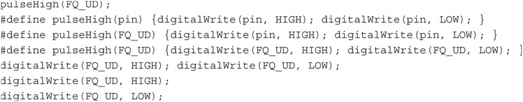
Note the use of both braces and parentheses in the statement lines. In other words, the single #define macro expands to two program statements. You could do away with the parameterized macro and simply use the last two statements with exactly the same result.
loop()
The first thing we do in loop() is see if the user has changed frequency using the encoder shaft. If the frequency has not changed, we go on to the next task. If it has changed we call NewShowFreq() to display the new frequency on the first line of the LCD display. DoRangeCheck() is then called to see if the new frequency is within a ham band. If not, an asterisk is displayed in column 1 of the first line on the LCD display. If we didn’t do this check-and-update sequence, you would likely be able to notice a little flicker in the display on each pass through loop(). If a new frequency has been set, the call to sendFrequency(currentFrequency) updates the AD9850 chip with the new frequency data.
Next, the code reads the current millisecond count via the call to millis(). If DELTATIMEOFFSET milliseconds (default is 10 seconds) have occurred since we last updated the current frequency stored in EEPROM, we call writeEEPROMRecord() to store that frequency in record 0 of the EEPROM memory space. However, because we don’t want to do EEPROM writes unless we have to, we check to see if the current frequency is different from the last frequency we wrote. If they are the same, no write is done and control reverts to loop(). If you turn off the VFO, it is this EEPROM frequency from record 0 that is used to initialize the display the next time your power up the VFO.
Note that we could have performed the frequency check in loop() just as well as in writeEEPROMRecord(). However, because loop() is going to execute many, many times before the user has a chance to change the frequency, we thought it would be slightly more efficient to check the elapsed time first, since that is the more restrictive condition.
The last thing that loop() does is check to see if any buttons have been pressed via a call to lcd.readButtons(). If so, the button code is passed to ButtonPush() for processing. All switches, SW1 through SW6, have their associated events processed in ButtonPush(). Although the function is fairly long, there is nothing in it that you haven’t seen before.
That’s all there is to it. Now all you have to do is test the VFO and then hook up your new VFO to your rig!
Testing the DDS VFO
The most obvious thing that you should be thinking about right now is how do I know if this thing is actually working correctly? Maybe you have a lab full of test equipment and the question is moot. You KNOW whether or not the DDS VFO is working. But, not having the proper test equipment is not an obstacle. Rather, it is an opportunity to be creative. But the first step is to get the software compiled and loaded before you think about testing anything. Remember that you must compile and load the EEPROM initialization program first and only then should you compile and load the main program.
Thanks to the generosity of the folks at Agilent Technologies, Dennis was loaned several of their 4000-series oscilloscopes for evaluation. The instrument pictured in Figure 16-17 is the MSO-X 4054A, a 500 MHz, 5 GS/sec digital storage oscilloscope. Dennis was able to use this scope in a number of projects and is considering purchasing one for his lab. This scope made design and testing much simpler than using his older HP 1742A scope.
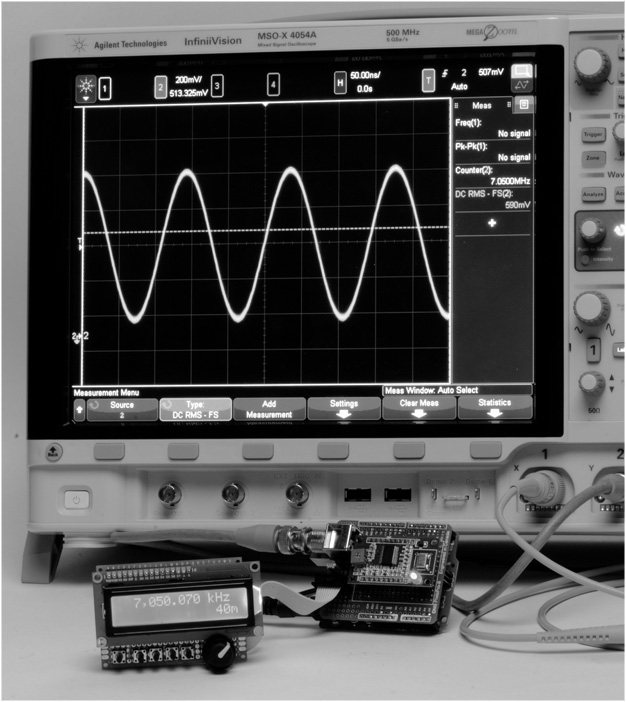
FIGURE 16-17 Output waveform of the DDS VFO.
Figure 16-18 shows a spectrum plot at 14.150 MHz from the DDS VFO. This display was captured using another Agilent instrument, an N9918A FieldFox. The plot shows that the second harmonic, at 28.325 MHz, is 49.6 dB below the fundamental. This is without any additional bandpass filtering on the output. This meets FCC Part 97 requirements for spectral purity in the amateur service, which is specified to be “at least 43 dB below the mean power of the fundamental emission.”

FIGURE 16-18 Spectrum display at 14.150 MHz.
The first step in testing, once the software is loaded, is to see that the user interface is operating correctly. This means that the Band+ and Band–, and the Step+ and Step– switches are all working correctly. Check that the shaft encoder is functioning by turning the encoder and checking that the frequency in the display increases and decreases. Now you can check that the memory functions are working.
If you are building this project, then you are also more than likely to own a receiver of some sort. Something that tunes the HF ham bands? There is your first means of testing the DDS VFO. The simple procedure is to connect a short piece of wire to the output connector of the DDS VFO and set the frequency to one that you can tune with your receiver. With the receiver set to receive CW or SSB, tune to the frequency you set. You may have to tune around a little bit depending on the accuracy of your receiver plus the frequency of the DDS may be off slightly. You should be able to detect a strong carrier on your receiver at the test frequency, meaning: Success!
Calibrating the DDS VFO
It is relatively simple to calibrate the frequency of the DDS VFO. Calibration does require an accurate receiver to note one frequency from the VFO. Lacking an accurate receiver, one that can receive WWV on one of their many frequencies can also be used. (WWV broadcasts on 2.5, 5, 10, 15, and 20 MHz.) For example, let’s use WWV transmitting on 10 MHz. Tune the receiver to 10 MHz in the AM mode. Using a wire connected to the output pin of the DDS VFO, wrap the wire around the antenna lead to your receiver. As you tune the DDS VFO near 10 MHz, what you hear is a beat note or heterodyne between the WWV carrier and the DDS VFO. Adjust the DDS VFO so that the beat note is as close to zero as you can. (That is, the note is so low that you can no longer hear it.) Record the displayed frequency on your VFO. What you now know is the displayed frequency for a 10 MHz signal. Chances are good that the DDS VFO does NOT display 10.000.000 MHz. Note the difference between the displayed frequency and 10 MHz. The difference is the calibration offset for your VFO.
The calibration offset is set using a #define statement:
![]()
A negative value is used when the display frequency is less than the output frequency. If the display frequency is greater than the output frequency, the value is positive. In the case of our DDS VFO, the offset is –100.
The software uses the following algorithm to calculate the data to load into the AD9850 to set the frequency. The AD9850 uses a 32-bit “tuning word” to set the frequency. The tuning word is a function of the desired frequency and the system clock. In our case the system clock is 125 MHz and the frequency is an unsigned long data type (32-bits). Analog Devices provides an algorithm in the AD9850 data sheet that we use:
![]()
where: Δ Phase is the 32-bit tuning word, CLKIN is the input reference clock in MHz, and ƒout is the output frequency in MHz.
We already know ƒout. What we want is the tuning word, so for our program, we rearrange the algorithm to provide the tuning word as the result. A little algebra and we end up with:
freq = (frequency + CALIBRATIONOFFSET) * 4294967295/125000000;
In decimal, 232 would normally be 4294967296. Since we are in a binary world using a 4-byte value that starts with “0,” the value actually used is (232 – 1) or 4294967295; all 1s. We express the clock frequency in Hertz (125000000) as well as the desired frequency: frequency.
We adjust the desired frequency adding CALIBRATIONOFFSET and the resulting tuning word, freq, is loaded into the AD9850.
Using the DDS VFO with Your Radio
Many QRP radios are crystal controlled and lack the ability to “tune around” even within a narrow frequency range. Some examples of this are the Pixie and the Blekok SSB radios. There are many others. This section describes how you can interface these and other radios to the DDS VFO project described in this chapter.
Any ham who started as Novice Class licensee in the days of “Incentive Licensing” was “rock bound” by regulation. Novice transmitters had to be crystal controlled. When the Novices moved up with their Technician or General Class licenses (or Advanced for that matter) they could now be “frequency agile” and use a VFO. The VFO plugged right into the crystal sockets on those old transmitters. The beauty of this was that the transmitter received new life! It did not have to be replaced right away. Novices could “stretch their legs” in the other portions of the bands now available due to their new frequency privileges.
The QRP community has embraced being rock bound for different reasons and not by regulation. A compact radio was the first order and crystal control lent itself well to building diminutive gear. Today, there is no reason that a crystal-controlled radio can’t be “unleashed” with a VFO, just like in the days of moving up from the Novice Class license. The process is to remove the crystal from the radio and replace it with the DDS VFO. The former crystal oscillator now functions in part as a buffer between the DDS VFO and the radio.
In many cases, all that is required is to remove the crystal and plug in the DDS VFO, as shown in Figure 16-19. The DDS VFO project is a generic VFO in that it produces a fundamental frequency for each of the MF and HF ham bands. The typical QRP rig is single band and uses the fundamental frequency. However, there are QRP and other rigs that you may wish to use this VFO with that do not use the fundamental frequency, but rather, they use a range of frequencies that are mixed with other oscillators to produce the fundamental frequencies for a particular ham band. This process was discussed in some detail in Chapter 15 when attaching the Arduino Frequency Counter to a double conversion radio. We provide guidance on how to change the frequency range of the DDS VFO for such an application.
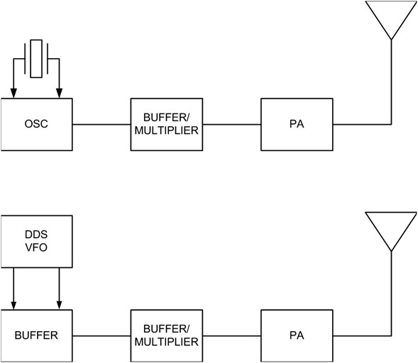
FIGURE 16-19 Connecting the DDS VFO to a typical radio.
The Pixie QRP Radio
The Pixie is an ingenious transceiver that really takes the “minimalist” approach to radio design. From what we can gather, the design originated in England in 1982 when George Burt, GM3OXX, wrote about the “Foxx” in the summer 1983 edition of SPRAT, The Journal of the G-QRP Club. The key feature of the design was the dual use of a single transistor as both PA and receiver mixer in a crystal controlled, direct conversion radio. The Foxx evolved into the Pixie and the Pixie has been evolving ever since. Today it is most commonly seen as the Pixie 2, consisting of one integrated circuit (an audio amplifier such as an LM386) and two transistors, one being the crystal oscillator and the other being the PA/mixer.
Today a Pixie 2 kit can be purchased on the Internet for as little as $9 and change. They are rockbound, often at a frequency of 7023 kHz. For our North American readers, this is in the Amateur Extra portion of the 40 meter band and not available to other license holders. In other parts of the world, however, this is a recognized 40 meter QRP frequency. Since most QRP activity takes place above 7040 kHz in North America, one must either replace the crystal with one more favorable to QRP operation in North America, or in either case (North America or elsewhere) add a VFO.
We secured two Pixie kits for 40 meters from eBay and assembled them. Assembly was quite straightforward and simple as this is a minimalist radio and has few parts. A partial schematic is reproduced in Figure 16-20 showing the crystal oscillator and PA, and how we connected the DDS VFO. The easiest way to add the DDS VFO is to disable the crystal oscillator by removing the oscillator transistor, Q1, and several surrounding components. The VFO is fed directly to the base of the PA/Mixer transistor, Q2, through capacitor C4.
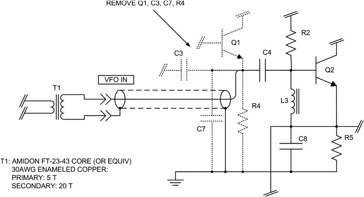
FIGURE 16-20 Modifying the Pixie 2 to add the DDS VFO.
We removed four components: Q1, C3, C7, and R4. When you build the kit, you can leave these four components out (along with the crystal Y1 and R1). If you have already built the kit, remove the four components indicated. They are shown in Figure 16-20 with dashed lines. Attach a piece of RG-174 to connect to the DDS VFO as shown in Figure 16-20.
In our testing, we discovered that the Pixie needs between 500 and 600 mV of drive at the base of Q2 for the receiver to function properly and for the transmitter to have the expected output. The DDS VFO may not have enough drive for this application so there are two alternatives. One alternative is to add the buffer stage described earlier in the chapter (Figure 16-10). Another option is to add a toroid transformer at T1 in Figure 16-20. T1 is designed to couple the output voltage of the DDS VFO. Wound on an Amidon FT-23-43 core, it has 5 turns for the primary and 20 turns for the secondary, both using 30AWG enameled copper wire. Follow the procedure described in Chapter 15 (Directional Wattmeter/SWR Indicator) for winding toroids and for tinning the ends. Count one turn each time the wire passes through the center of the core and use a soldering iron to burn the insulation off of the end of each wire. The transformer is installed on the DDS shield between the output of the DDS breakout module and the output connector.
This method of attaching the DDS VFO to a radio in place of a crystal oscillator is usable for other radios for which you may wish to use the DDS VFO. Oftentimes, removing the crystal oscillator and installing the DDS VFO in its place is a good solution.
Blekok Micro 40SC
The Blekok Micro 40SC is a 40 meter Single Sideband (SSB) and CW QRP transceiver developed in Indonesia by Indra Ekoputro, YD1JJJ. Jack recently obtained his from eBay and we have found that it has good sensitivity and selectivity but the VFO can be a bit touchy. We have made minor modifications to the Micro 40SC, which allow the addition of the Arduino DDS VFO. The modifications include removing a 100 pF SMT capacitor and inserting a 2-pin header in a marked spot already silk screened on the printed circuit board.
The Micro 40SC uses an SA602 as mixer and VFO. The modifications, shown in Figure 16-21, and visible in the photographs in Figure 16-22, showing the chip cap removed, and Figure 16-23, showing the location of the new 2-pin header.
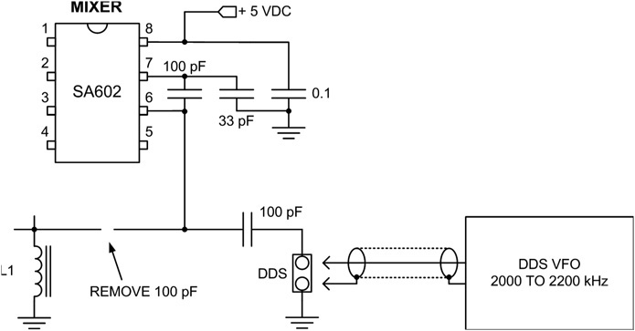
FIGURE 16-21 Modifying the Blekok Micro 40SC for use of the DDS VFO.
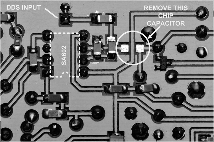
FIGURE 16-22 Remove the 100 pF SMT capacitor from this location.
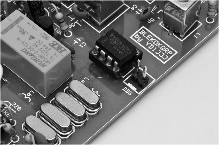
FIGURE 16-23 Two-pin header added for the DDS VFO input.
CRKits CRK 10A 40 meter QRP Transceiver
The CRK 10A is another inexpensive, highly portable QRP CW transceiver that operates on a fixed, crystal controlled frequency. The CRK 10 A is very easy to modify to use the DDS VFO for frequency control. The modifications remove the crystal, and install a capacitor and a connector for the VFO input.
Figure 16-24 shows a partial schematic of the CRK 10A and shows where the DDS VFO connects. We attached the coax as shown in Figure 16-25. We used a length of RG-174 with a BNC connector, drilled a ![]() -in. hole in the rear panel, and ran the coax to the pads that were for the crystal we removed, X3. The RG-174 is routed under the circuit board as shown in Figure 16-25. In the photograph, the center conductor is the lead on the left. We wrapped a piece of AWG22 solid wire around the shield braid, soldered the connection, and then covered it with heat-shrink tubing so that it would not short to the circuit board. The solid wire is covered with a piece of Teflon tubing, the same materials we use for wiring most of our shields.
-in. hole in the rear panel, and ran the coax to the pads that were for the crystal we removed, X3. The RG-174 is routed under the circuit board as shown in Figure 16-25. In the photograph, the center conductor is the lead on the left. We wrapped a piece of AWG22 solid wire around the shield braid, soldered the connection, and then covered it with heat-shrink tubing so that it would not short to the circuit board. The solid wire is covered with a piece of Teflon tubing, the same materials we use for wiring most of our shields.
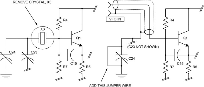
FIGURE 16-24 Partial schematic of CRK 10A showing connection for DDS VFO.

FIGURE 16-25 Modifications performed on the CRK 10A transceiver.
Other Applications of the DDS VFO and Additional Enhancements
The DDS VFO shown in this chapter can be used for a variety of applications. By adding an output attenuator, it becomes a low-cost RF signal generator with a range of 1.6 MHz to 30 MHz. The DDS VFO is not limited to use with QRP rigs either. It is also compatible with vacuum tube equipment, given one minor modification. The DDS VFO as it stands generates just under 1 V peak-to-peak output. A typical vacuum tube circuit requires a bit higher voltage, usually 6 to 8 V peak-to-peak. We showed one version that uses an output buffer stage, but to get the output to 8 Volts, the easiest solution is to add a toroid transformer on the output. Using a small toroid such as an Amidon FT-23-43, wind 5 turns for the primary and 20 turns for the secondary using 30 AWG enameled wire. This roughly doubles the output voltage and is more suitable for driving most tube type equipment.
There are some enhancements that can be added to the DDS VFO with minor changes to the software and hardware. One such modification would be to add a frequency offset while transmitting. By sensing when transmitting (using a digital input on the keying circuit) it is possible to slightly shift the transmitted frequency. Another possible enhancement would be to add a Receiver Incremental Tuning or RIT control in addition to the transmit sense. The RIT control can use a pot and an analog input to adjust the receive frequency over a range of 1 to 2 kHz.
Conclusion
As you can see, this is a versatile project with many uses with many pieces of equipment. Maybe you want to build a new transmitter or receiver. The DDS VFO provides a low-cost stable source of low-level RF in the HF ham bands.