 CHAPTER 9
Using Reconfigurable Computing for the Optimization of Cryptographic Algorithms
J. M. GRANADO, M. A. VEGA, J. M. SÁNCHEZ, and J. A. GÓMEZ
Universidad de Extremadura, Spain
9.1 INTRODUCTION
Cryptography is a tool used since the early days of civilization: for example, to avoid the enemy reading messages from captured emissaries. Nowadays, the Internet has made it necessary to employ cryptography to transmit information through an insecure channel. One of the first cryptography machines was Enigma, which employs rotor machines to make the encryption, early in the twentieth century. Later, with the appearance of computers, the cryptographic algorithms became more complex. Nowadays, secure algorithms such as DES, Triple-DES, and IDEA exist. Finally, with the appearance of wireless networks, new specific cryptographic algorithms have been developed to be used in these networks, such as MARS, SERPENT, RC6, or Rijndael, which has turned into the new AES standard. Besides, due to the new fast network standards, these algorithms must be very fast, and a very interesting solution is to implement them using hardware such as field-programmable gate arrays (FPGAs). At this point we can find works [2,11,28] in which FPGA-based implementations of IDEA, AES, and RC6 algorithms are described, respectively. We have implemented these algorithms using FPGAs, achieving very good results in all of them, as we will see in the next sections.
The chapter is structured as follows. In Section 9.2 we describe the three cryptographic algorithms implemented. Next we explain the solutions and component implementation within an FPGA. In Section 9.4 the results are shown. Finally, we describe the conclusions obtained.
9.2 DESCRIPTION OF THE CRYPTOGRAPHIC ALGORITHMS
Next, we describe the IDEA, AES, and RC6 algorithms.
9.2.1 IDEA Algorithm
The international data encryption algorithm (IDEA) [22] is a 64-bit block cryptographic algorithm that uses a 128-bit key. This key is the same for both encryption and decryption (it is a symmetric algorithm, and it is used to generate fifty-two 16-bit subkeys). The algorithm consists of nine phases: eight identical phases [Figure 9.1(a)] and a final transformation phase [Figure 9.1(b)]. The encryption takes place when the 64-bit block is propagated through each of the first eight phases in a serial way, where the block, divided into four 16-bit subblocks, is modified using the six subkeys corresponding to each phase (elements ![]() of Figure 9.1: six subkeys per phase and four subkeys for the last phase). When the output of the eighth phase is obtained, the block goes through a last phase, the transformation one, which uses the last four subkeys.
of Figure 9.1: six subkeys per phase and four subkeys for the last phase). When the output of the eighth phase is obtained, the block goes through a last phase, the transformation one, which uses the last four subkeys.
The decryption follows an identical pattern but computing the sum or multiplication inverse of the subkey, depending on the case, and altering the order of use of the subkeys. As we can suppose, the major problem in the FPGA implementation of this algorithm lies in the multipliers, since apart from taking a great amount of computation and resources, they are executed four times in each phase. The improvement of this component is one of the most studied aspects of the literature. In our case we use KCM multipliers and partial and dynamic reconfiguration.
9.2.2 128-Bit AES Algorithm
The advanced encryption standard (AES) [9] is a symmetric block cipher algorithm that can process data blocks of 128 bits using cipher keys with lengths of 128, 192, and 256 bits. This algorithm is based on the Rijndael algorithm [7], but Rijndael can be specified with key and block sizes in any multiple of 32 bits, with a minimum of 128 bits and a maximum of 256 bits. In our case, we have used a 128-bit key.
The AES algorithm is divided into four phases, which are executed sequentially, forming rounds. The encryption is achieved by passing the plain text through an initial round, nine equal rounds and a final round. In all of the phases of each round, the algorithm operates on a 4 × 4 array of bytes (called the state). In Figure 9.2 we can see the structure of this algorithm. Reference 8 provides a complete mathematical explanation of the AES algorithm. In this chapter we explain only the MixColumns phase of the algorithm in more detail because it will be necessary to understand its implementation.
MixColumns Phase The MixColumns transformation operates on the state column by column, treating each column as a four-term polynomial. The columns are considered as polynomials over GF(28) and multiplied modulo x4 + 1 by a fixed polynomial a(x), given by

Figure 9.1 Description of the IDEA cryptographic algorithm phases: (a) normal phase; (b) transformation phase.

Figure 9.2 Description of the AES cryptographic algorithm.
This can be written as a matrix multiplication:
As a result of this multiplication, the four bytes in a column are replaced as follows:
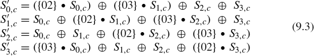

Figure 9.3 The xtime function.
where ⊕ represents the XOR operation and ![]() is a multiplication modulo the irreducible polynomial m(x) = x8 + x4 + x3 + x + 1. Figure 9.3 shows the implementation of the function B = xtime(A), which is used to make multiplications of a number by 2 modulo m(x). So we will only have binary operations:
is a multiplication modulo the irreducible polynomial m(x) = x8 + x4 + x3 + x + 1. Figure 9.3 shows the implementation of the function B = xtime(A), which is used to make multiplications of a number by 2 modulo m(x). So we will only have binary operations:

9.2.3 128-Bit RC6 Algorithm
RC6 [19] is a symmetric cryptographic algorithm and one of the five finalists of the advanced encryption standard (AES) competition [16]. It was also submitted to the New European Schemes for Signatures, Integrity and Encryption (NESSIE) [5] and the Cryptography Research and Evaluation Committee (CRYPTREC) [6] projects. It is a proprietary algorithm, patented by RSA Security [20]. This algorithm can employ different block and key sizes, depending on three parameters:
- w: the word size in bits
- r: the number of rounds made by the algorithm
- b: the length of the encryption key in bytes
So the RC6 versions are denoted by RC6-w/r/b. In our case we use the version established by AES, that is, w = 32 (128-bit data), r = 20 (20 loop rounds), and b = 16 (128-bit key). So in the future we call RC6 to the RC6-32/20/16 version. In all versions of this algorithm, the following operations are used:
- a + b: integer addition modulo 2w (232 in our case).
- a − b: integer subtraction modulo 2w (232 in our case).
- a ⊕ b: bitwise exclusive-or.
- a × b: integer multiplication modulo 2w (232 in our case).
- a < < < b: rotate the word a to the left by the amount given by the least significant lg2 w bits of b (the least significant 5 bits of b in our case).
- a > > > b: rotate the word a to the right by the amount given by the least significant lg2 w bits of b (the least significant 5 bits of b in our case).
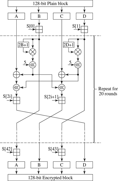
Figure 9.4 RC6 encryption algorithm.
RC6 works with four w-bit registers/words (A, B, C, and D), which contain the initial input plaintext as well as the output cipher text at the end of encryption. To encrypt a block, we will pass it through a loop of r iterations (in our case, 20) in which two subkeys are used per iteration. Besides, two subkeys operate before the loop and two after the loop. The algorithm can be seen in Figure 9.4. The decryption algorithm is practically equal to the encryption, but executing the operations in the inverse order. Besides, the additions are replaced by subtractions and the third and fourth left rotations of each round are replaced by right rotations.
9.3 IMPLEMENTATION PROPOSAL
To implement the cryptographic algorithms described previously, we combine three different techniques: partial and dynamic reconfiguration, pipelining, and in the IDEA case, parallelism. Let us see how we have implemented each algorithm. In all cases we employ VHDL [18] to implement the reconfigurable elements, Handel-C [3] to implement nonreconfigurable elements, and JBits [24] to make the partial and dynamic reconfiguration. On the other hand, a Virtex-II 6000 FPGA [27] has been employed to implement all the algorithms.
9.3.1 Implementation of the IDEA
To implement the IDEA, we have used constant coefficient multipliers (KCMs) [25] and constant coefficient adders (KCAs) [12]. These elements operate a variable datum with a constant datum, and as we can see in Figure 9.1, all the multipliers and several adders of the IDEA algorithm operate with a constant. Thanks to these elements, we reach a high performance level since KCMs are much faster than the traditional multipliers (KCAs are only a little faster than normal adders, but we need them to do the key reconfiguration and reduce the clock cycle). We have employed an inner pipelining in the IDEA. This pipelining is done in the KCM and KCA elements since they are the slowest.
KCM and KCA Pipelining In the KCM as we can see in Figure 9.5 (a detailed explanation of KCM implementation is given in ref. 12), we have used a total of six stages and several pipelining registers (one 32-bit register, six 20-bit registers, eight 16-bit registers, two 4-bit registers and five 1-bit registers) to execute the KCM completely. On the other hand, we use only four stages to execute the KCA completely, and the number of pipelining registers is also lower (one 19-bit register, three 5-bit registers, and five 4-bit registers), as we can see in Figure 9.6 (ref. 12 includes a detailed explanation of the KCA implementation). As we said previously, this component is not much faster than a normal adder, but it allows us to increment the clock frequency (because it uses small adders) and to make the key reconfiguration.
Operation Pipelining Besides the inner pipelining, we use an operation pipelining. This pipelining is done among all simple operations (e.g., adders or XORs) of all the phases of the IDEA: In Figure 9.7 we can see how several pipelining registers are included to wait for the result of the KCMs because these elements have the majority of pipelining stages of the algorithm.
We can see that the pipelining done is a very fine grain (the total number of pipelining stages is 182), which greatly reduces the clock frequency (the clock frequency is 4.58 ns). This fact leads to a high latency (182 cycles), but if we are encrypting a great number of blocks, the benefit achieved by the high clock frequency clearly overcomes the disadvantage of the latency.
Dual Path Finally, we have implemented two separate and parallel data paths, a reason why we encrypt two blocks at the same time, that is, two blocks per cycle. Besides, these data paths allow us both to duplicate the performance of the encryption/decryption by means of reconfiguring the KCM and KCA with the same subkeys and to use one path to encryption and another to decryption. This last option is best in case the FPGA is installed into a server that has the responsibility of encrypting the data coming from an extranet (e.g., the Internet) to, for example, a wireless insecure intranet, and vice versa.

Figure 9.5 KCM pipelining.
9.3.2 Implementation of the AES Algorithm
Opposite to the IDEA, AES does not have complex operations, but on the other hand, it has a high memory cost. If we want to do the transformation of all bytes of the state in the SubByte phase in a parallel way, we must implement 16 SBox by phase. Besides, if we want to implement a pipelined version of the algorithm, we must implement 10 SubByte phases, each of which has 16 SBox tables. Furthermore, as we want to implement a pipelined version, we must define 11 4 × 4 1-byte subkeys, because we have 11 AddRoundKey phases. All these storing elements give us a total of 329,088 bits (= 10 SubBytePhases × 16 SBoxTablesPerSubBytePhase × 256 ElementsPerSBox × 8 BitsPerElement + 11 AddRoundKeyPhases × 16 ElementsPerAddRoundKeyPhase × 8 BitsPerElement). On the other hand, we have only forty-one 128-bit pipelining registers (Figure 9.8), less than for the IDEA.
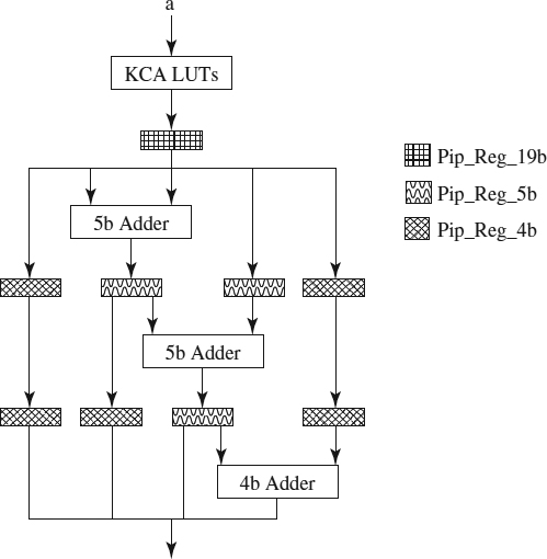
Figure 9.6 KCA pipelining.
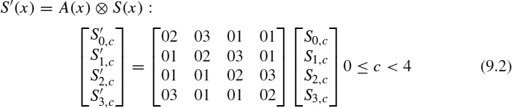
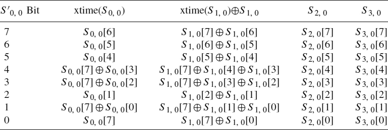
MixColumns Phase Implementation As we have said, the AES algorithm has no complex phases, and the implementation of all of them is very simple. However, the MixColumns phase implementation deserves special consideration. Formerly, we saw a brief mathematical description of this phase and now we will see how to implement it. To explain the implementation, we take the calculation of the element S′0, 0 of the S′(x) matrix (Equation 9.2). The equation to solve this element is
Let us remember that the ![]() operation is done by means of the xtime function (Equation 9.2). So Equation 9.5 changes to
operation is done by means of the xtime function (Equation 9.2). So Equation 9.5 changes to
Finally, taking into account the representation of the xtime function in Figure 9.3, we will use the final result described in Table 9.1 (the result of bit n will be the XOR among the four columns of row n).
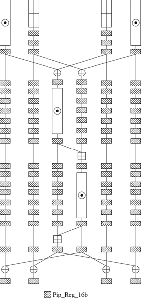
Figure 9.7 Operation pipelining of one phase of the IDEA.
KeyExpansion Phase Observing Figure 9.2, we can see that the KeyExpansion phase calculates the subkeys that will be used by the different AddRoundKey phases. However, we do not implement this method; instead, we use partial reconfiguration. The process is similar to the IDEA run-time reconfiguration, but in this case, we reconfigure the LUTs that will be used in the AddRoundKey phases (i.e., the LUTs that store the subkeys) instead of the components that use these LUTs (as happens in the IDEA).
AES Pipelining As we did in the IDEA, we use operation-level pipelining. However, as in the AES algorithm, all the operations of one phase (remember that in the AES algorithm, a round has several phases; see Figure 9.2) are done at the same time, actually, it is phase-level pipelining. This pipelining can be seen in Figure 9.8.
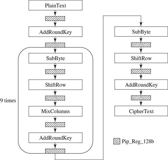
Figure 9.8 Phase-level pipelining of the AES algorithm.
TABLE 9.1 Calculation of the State's S′0, 0 Byte in the MixColumns Phase
9.3.3 Implementation of the RC6 Algorithm
In this case, the critical element is the multiplier, but opposite to the IDEA, both input data are variable. However, the subkeys are used in the adders, but in this case, 32-bit adders (in the IDEA we used 16-bit adders), which is why we use a variation of the IDEA KCAs. Let us see how we have implemented these elements.
32-Bit Adders To implement these elements, we have designed a 32-bit KCA based on the 16-bit IDEA KCA. So we are going to implement two slightly different 16-bit IDEA KCAs: The first, the least significant, will return 17 bits, that is, 16 bits for the addition of the 16 least significant bits and 1 bit for the output carry, and the second adder, the most significant, will return 16 bits, that is, the addition of the 16 bits most significant and the previous output carry. Implementation of these two elements can be seen in Figures 9.9 and 9.10.
In the figures the 4 × 5 LUTs return 4 bits related to the addition and one bit related to the carry. The four LSBs of each 4 × 5 LUT are used to generate a 16-bit operand, and the carry bits of the four LUTs plus the input carry in the most significant KCA are used to generate another 16-bit operand. Finally, these two operands are added, calculating the two 16-bit parts of the operation, and the complete 32-bit adder will be the result of joining the output data of the two KCAs. The resulting circuit can be seen in Figure 9.11. It is important to emphasize that the second adder uses a 4 × 4 LUT (the most significant one) because the adder is modulo 232, so the carry is discarded.

Figure 9.9 Least significant KCA with output carry.
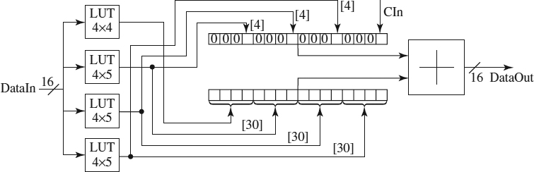
Figure 9.10 Most significant KCA with input carry.

Figure 9.11 32-bit complete KCA.
32-Bit Multipliers In this algorithm the multipliers are the critical elements, so it is important to implement them in an efficiently. To implement the multipliers we have used the MULT18x18s (18 × 18 bit multipliers) embedded in the Virtex-II 6000 FPGA [27].
Before beginning the multiplier design, we must take into account two facts: First, we have 18 × 18 multipliers, so we are going to divide the multiplication by parts using the divide-and-conquer method [17]; and second, the multiplication is modulo 232, so several operation bits will be discarded.
Now we can begin to design the circuit. As we have said, we have employed the divide-and-conquer method but have modified it because the multiplication is modulo 232. In the original divide-and-conquer algorithm

the subscript indicates the size in bits of the operand and the superscript indicates either the high or low part of the operand. This equation shows the original divide-and-conquer method, but as we have multiplications modulo 232, Equation 9.7 is replaced by

Now, we need only add the multiplications, but not all the bits are used. The bits involved in the multiplication can be seen in Figure 9.12. So we have three 16-bit multipliers and two 16-bit adders instead of the four 16-bit multipliers and three 32-bit adders of the original divide-and-conquer method. Therefore, the final circuit of the multiplier modulo 232 is shown in Figure 9.13.

Figure 9.12 Addition modulo 232 of the partial multiplications.

Figure 9.13 Complete multiplier modulo 232.
RC6 Pipelining Until now we have explained how the operators are implemented. Now we are going to see how we have used pipelining to encrypt several parts of several blocks at the same time. We have implemented a middle-grain pipelining because the critical elements, that is, the MULT18x18s multipliers, expend more time than do the remaining elements, which is why we have preferred to balance the pipelining. Figure 9.14 shows the pipelining implementation. Also, the multipliers are actually pipelined, using two phases to complete the operation. So the final pipelined implementation has a total of 82 stages, where each round of the main loop has four of these stages, and the total number of 32-bit pipelining registers is 484 (each multiplier has three inner registers).
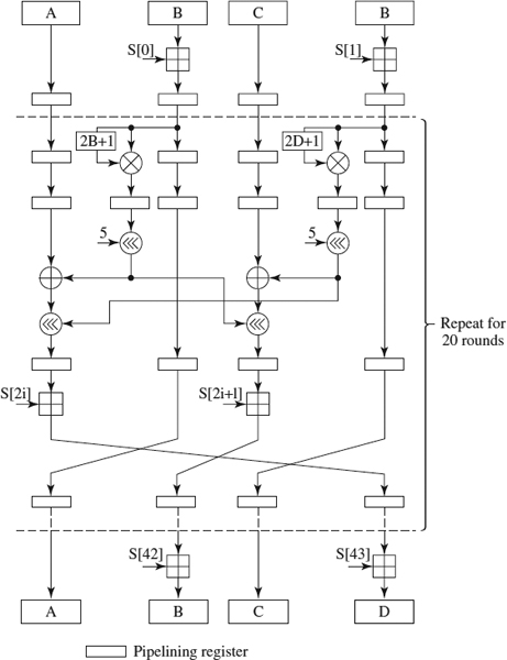
Figure 9.14 Final pipelined implementation for the RC6 algorithm.
9.4 EXPERMENTAL ANALYSIS
To obtain the following results, in all the cases we have used Xilinx ISE 8.1i and Celoxica DK4.
9.4.1 IDEA Results
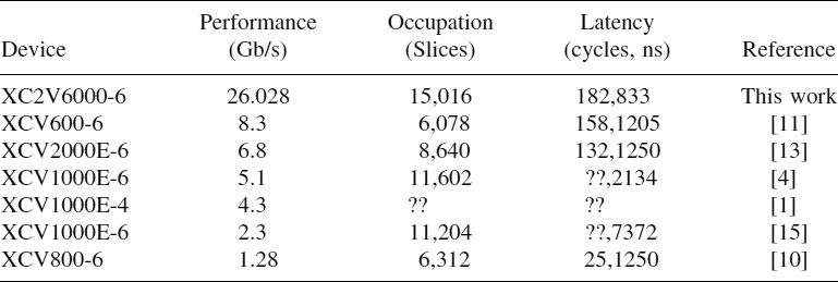
After synthesis with Xilinx ISE, our implementation takes only 45% of the FPGA slices (exactly 15,016 slices) and has a clock of 4.58 ns. In conclusion, after the initial latency, it encrypts two 64-bit blocks every 4.58 ns. This gives us a total performance of 26.028 Gb/s, surpassing the best results achieved by other authors, as Table 9.2 shows. In addition, our results are better than the results of other authors in the latency. It is important to emphasize that although we have a high latency (182 cycles), which is bad for small data size encryption, the applications usually encrypt data of great size, particularly when are speaking of an encryption server. On the other hand, we have a double data path, and therefore our occupation and latency (in Table 9.2) encrypt two data blocks (other authors encrypt only one block).
TABLE 9.2 Comparative Results of the IDEA
9.4.2 AES Results
Now let's look at the AES results. Our implementation uses a total of 3720 slices, only 11% of the FPGA resources. This result is one of the best in that field, as we can see in Table 9.3 (it is important to emphasize that Table 9.3 does not include the slices or BRams which are used for the SBox storage because these data are very similar for all the implementations). On the other hand, thanks to the pipelined implementation, we can reach a clock cycle of 5.136 ns, that is, a performance of 23.211 Gb/s. This datum is not the best of Table 9.3 (it is the second best), but we improve the work [28] in the rest of columns of this table, so our result is comparable with the ref. [28] implementation and better than implementations by other authors. Finally, the latency column is also favorable to us, where we again have the best result.
9.4.3 RC6 Results
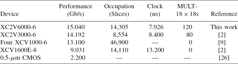
As we can see in Table 9.4, our implementation employs a total of 14,305 slices and reaches a clock of 7.926 ns, the best in the table. This clock allows us to achieve a performance of 15.040 Gb/s, surpassing the results reached by the other authors.
9.5 CONCLUSIONS
In this work we have presented the FPGA-based implementation of three important cryptographic algorithms (IDEA, AES, and RC6) using partial and dynamic reconfiguration, pipelining, and in the IDEA case, parallelism. To implement these algorithms we have used a Virtex-II 6000 FPGA, VHDL and Handel-C as hardware description languages, and JBits to make the runtime reconfiguration. Taking all of these into account, we have reached very fast implementations of the three algorithms, so we can say that the techniques used in this work to implement cryptographic algorithms, that is, pipelining, parallelism, and partial and dynamic reconfiguration, are very good techniques for optimizing cryptographic algorithms.
TABLE 9.3 Comparative Results of the AES Algorithm

TABLE 9.4 Comparative Results of the RC6 Algorithm
Acknowledgments
The authors are partially supported by the Spanish MEC and FEDER under contract TIC2002-04498-C05-01 (the TRACER project).
REFERENCES
1. J. Beuchat, J. Haenni, C. Teuscher, F. Gómez, H. Restrepo, and E. Sánchez. Approches met érielles et logicielles de l'algorithme IDEA. Technique et Science Informatiques, 21(2):203–204, 2002.
2. J. Beuchat. High Throughput Implementations of the RC6 Block Cipher Using Virtex-E and Virtex-II Devices. Institut National de Recherche en Informatique et en Automatique, Orsay, France, 2002.
3. Celoxica. Handel-C Language Reference Manual, version 3.1. http://www.celoxica.com, 2005.
4. O. Cheung, K. Tsoi, P. Leong, and M. Leong. Tradeoffs in parallel and serial implementations of the international data encryption algorithm (IDEA). Workshop on Cryptographic Hardware and Embedded Systems, 2162:333–347, 2001.
5. Computer Security and Industrial Cryptography. https://www.cosic.esat.kuleuven.be/nessie, 2007.
6. Cryptography Research and Evaluation Committees. http://www.cryptrec.jp, 2007.
7. J. Daemen and V. Rijmen. The block cipher Rijndael. Lecture Notes in Computer Science, 1820:288–296, 2000.
8. Federal Information Processing Standards Publication 197. http://csrc.nist.gov/publications/fips/fips197/fips-197.pdf, 2001.
9. K. Gaj and P. Chodowiec. Fast implementation and fair comparison of the final candidates for advanced encryption standard using field programmable gate arrays. Lecture Notes in Computer Science 2020:84–99, 2001.
10. I. González. (2002) Codiseño en sistemas reconfigurables basado en Java. Internal Technical Report, Universidad Autonoma de Madrid, Spain.
11. I. González, S. Lopez-Buedo, F. J. Gómez, and J. Martínez. Using partial reconfiguration in cryptographic applications: an implementation of the IDEA algorithm. In Proceedings of the 13th International Conference on Field Programmable Logic and Application, pp. 194–203, 2003.
12. J. M. Granado-Criado, M. A. Vega-Rodríguez, J. M. Sánchez-Pérez, and J. A. Gómez-Pulido. A dynamically and partially reconfigurable implementation of the IDEA algorithm using FPGAs and Handel-C. Journal of Universal Computer Science, 13(3):407–418, 2007.
13. A. Hamalainen, M. Tomminska, and J. Skitta. 6.78 Gigabits per second implementation of the IDEA cryptographic algorithm. In Proceedings of the 12th International Conference on Field Programmable Logic and Application, pp. 760–769, 2002.
14. A. Hodjat and I. Verbauwhede. A 21.54 Gbits/s fully pipelined AES processor on FPGA. In Proceedings of the 12th Annual IEEE Symposium on Field-Programmable Custom Computing Machines, 2004.
15. M. P. Leong, O. Y. Cheung, K. H. Tsoi, and P. H. Leong A bit-serial implementation of the international data encryption algorithm (IDEA). In Proceedings of the IEEE Symposium on Field-Programmable Custom Computing Machines, pp. 122–131, 2000.
16. National Institute of Standards and Technology. http://csrc.nist.gov/archive/aes/index.html, 2007.
17. B. Parhami. Computer Arithmetic. Oxford University Press, New York, 2000.
18. V. A. Pedroni. Circuit Design with VHDL. MIT Press, Cambridge, MA, 2004.
19. R. Rivest, M. Robshaw, R. Sidney, and Y. Yin. The RC6 block cipher. http://www.rsa.com/rsalabs/node.asp?id=2512, 2007.
20. RSA security. http://www.rsa.com, 2007.
21. G. P. Saggese, A. Mazzeo, N. Mazzoca, and A. G. Strollo. An FPGA-based performance analysis of the unrolling, tiling, and pipelining of the AES algorithm. Lecture Notes in Computer Science, 2778:292–302, 2003.
22. B. Schneier. Applied Cryptography, 2nd ed. Wiley, New York, 1996.
23. F. X. Standaert, G. Rouvroy, J. Quisquater, and J. Legat. Efficient implementation of Rijndael encryption in reconfigurable hardware: improvements and design tradeoffs. Lecture Notes in Computer Science, 2779:334–350, 2003.
24. JBits User Guide. Sun Microsystems, 2004.
25. R. Vaidyanathan and J. L. Trahan. Dynamic Reconfiguration: Architectures and Algorithms. Kluwer Academic/Plenum Publishers, New York, 2003.
26. B. Weeks, M. Bean, T. Rozylowicz, and C. Ficke. (2000) Hardware performance simulations of round 2 advanced encryption standard algorithms. Technical Report. National Security Agency, Washington, DC
27. Virtex-II Platform FPGAs: Complete Data Sheet. Xilinx, 2005.
28. S. M. Yoo, D. Kotturi, D. W. Pan, and J. Blizzard. An AES crypto chip using a high-speed parallel pipelined architecture. Microprocessors and Microsystems 29(7):317–326, 2005.
Optimization Techniques for Solving Complex Problems, Edited by Enrique Alba, Christian Blum, Pedro Isasi, Coromoto León, and Juan Antonio Gómez
Copyright © 2009 John Wiley & Sons, Inc.