
14
Numerical Computation of High-Voltage Field by Finite Difference Method
ABSTRACT Numerical methods for solving Laplace’s equation by expressing it in finite-difference form have been attempted by researchers way back in the mid-1950s. However, it is only in the mid-1960s, with the advent of relatively high-speed computers, that this numerical method of solution became a feasible proposition. Finite difference method (FDM), as it is commonly known, could be used to study electrostatic field distribution in two-dimensional (2D), axi-symmetric as well as in three-dimensional (3D) cases. This chapter presents detailed discussions on the FDM formulations as applied to all the above-mentioned cases. The system of FDM equations, the accuracy criteria as well as the technique to handle unbounded field region problems have been discussed thoroughly. Suitable application examples of 2D and axi-symmetric case studies are also given that show typical FDM grids for easy comprehension of FDM methodology.
The principle of finite difference method (FDM) is to discretize the entire region under study and solve for unknown potentials a set of coupled simultaneous linear equations, which approximate Laplace’s or Poisson’s equations. In fact, this is the objective of most of the numerical-field computation techniques that are being used at present. In FDM, for a two-dimensional (2D) system, the entire region of interest (ROI) is discretized using either rectangles or squares. In a three-dimensional (3D) system, the discretization is done using either rectangular parallelepipeds or cubes. Most commonly, electric potential is assumed to vary linearly between two successive nodes. However, this is not mandatory. Any other type variation, for example, quadratic or polynomial, may also be assumed. But, a complex nature of potential variation increases the computational burden greatly and may not always give improved accuracy. If the electric potential is assumed to vary linearly, as it is commonly considered, then the nodes need to be closely spaced where the field varies significantly in space. This is generally the case near the electrodes or dielectric boundaries, particularly in the cases of contours having sharp corners. On the other hand, in the region away from the electrodes or dielectric boundaries, where the field does not change rapidly in space, the nodes may be spaced relatively widely apart. For multi-dielectric problems, care should be taken during discretization to make sure that only one dielectric is present between two consecutive nodes. This is achieved by arranging one layer of nodes along the dielectric–dielectric interface. This aspect will be taken up in more details in a Sections 14.4 and 14.5 in this chapter.
As stated earlier, in a 3D system, discretization is done using either rectangular parallelepipeds or cubes. In such cases, one particular node is connected to six neighbouring nodes, as shown in Figure 14.1. As it is assumed that electric potential varies linearly between two successive nodes, it is obvious that the potential of that particular node will be related to potentials of the six connected nodes. FDM equation for any unknown node potential is developed in terms of potentials of the connected nodes by satisfying Laplace’s equation. FDM equation thus developed is a linear equation, that is an approximation of Laplace’s equation, which is a second-order partial differential equation. FIGURE 14.1 Because the nodal distances in a practical system are unequal, the following approach is normally taken for the development of the FDM equations. After discretization, the largest nodal distance (h) is identified within the ROI. Then all the other nodal distances are represented as a fraction of that largest nodal distance as sxh, where sx < 1. This is done because the factor sx is a dimensionless quantity and the FDM equation is developed in terms of potentials of the six connected nodes and the dimensionless factors sx. Therefore, the developed FDM equation becomes a linear equation involving electric potential only. As shown in Figure 14.1, the unknown potential of node 0 will be formulated in terms of potentials of the six connected nodes 1 through 6. Electric potential being a continuous function within the ROI and the nodal distances being not large, the Taylor series can be applied for the determination of the potential of any one connected node from the potential of node 0. Taylor series in 3D system is expressed as follows: Applying the Taylor series expansion between nodes 1 and 0 considering the potential of node 0 (V0) as f(x,y,z) and the node potential of node 1 (V1) as f(x + a,y + b,z + c), so that a = s1h, b = c = 0 and neglecting higher order terms, Similarly, applying the Taylor series expansion between nodes 0 and 3, such that a = −s3h, b = c = 0. Eliminating ∂V/∂x from Equations 14.2 and 14.3, Similarly, between nodes 2 and 4 in the y-direction, and between nodes 5 and 6 in the z-direction, Now, Laplace’s equation in the Cartesian coordinates at node 0, Therefore, from Equations 14.4 through 14.7, eliminating h, the FDM equation for the unknown node potential V0 is obtained as For equal nodal distances in a 3D system, s1 = s2 = s3 = s4 = s5 = s6 = 1. Therefore, Equation 14.8 reduces to For a 2D system, as shown in Figure 14.2, with unequal nodal distances, the FDM Equation 14.8 reduces to FIGURE 14.2
For equal nodal distances in a 2D system, the FDM Equation 14.10 reduces to Consider the 3D arrangement with single dielectric having six given planes a, b, c, d, e and f, as shown in Figure 14.3. Write the FDM equations for the unknown node potentials V01 and V02. Given h2 = 0.6 h1. Solution: In this case, for both the nodes 01 and 02, s1 = s2 = s3 = s4 = 1 and s5 = s6 = (h2/h1) = 0.6. and FIGURE 14.3 For the 2D system with single dielectric, as shown in Figure 14.4, write the FDM equations for the unknown node potentials. Boundary node potentials are given in the figure. Solution: From Figure 14.4, it may be seen that for nodes 1, 2, 4 and 5, the nodal distances are equal, that is, h = r/2. For node 3, s1 = s3 = s4 = 1 and s2 can be computed trigonometrically as 0.268, as s2h = (r − r cos θ) and sin (θ) = (h/r). Moreover, for nodes 1 and 2, symmetry with respect to the central plane is to be considered, such that for node 1 another node on the left-hand side has to be considered whose potential will be equal to V4 and similarly for node 2. FIGURE 14.4
When the field is expressed in cylindrical coordinates (r,θ,z) and the field distribution is independent of ‘θ’, then the field distribution is said to be axi-symmetric or rotationally symmetric, for example, insulators, bushings and so on. A typical diagram of an axi-symmetric object is shown in Figure 14.5. To determine the electric field distribution in an axi-symmetric system, Laplace’s equation in cylindrical coordinates, as given below, needs to be solved. In an axi-symmetric system, V is independent of θ, so that Equation 14.15 reduces to FIGURE 14.5 In FDM, for an axi-symmetric system, the ROI is discretized using either rectangles or squares. In such cases, one particular node is connected to four neighbouring nodes, as shown in Figure 14.6. As it is assumed that electric potential varies linearly between two successive nodes, it is obvious that the potential of that particular node will be related to potentials of the four connected nodes. FDM equation for any unknown node potential is developed in terms of potentials of the connected nodes by satisfying Laplace’s equation in cylindrical coordinates. Figure 14.6 shows node 0 with unknown potential lying at a certain distance away from the axis of symmetry. In such a case, the radial distance of node 0 from the axis of symmetry is also taken as multiple (sh) of the largest nodal distance h. From the Taylor series expansion between nodes 1 and 0 in the r-direction, neglecting higher order terms, Similarly, from the Taylor series expansion between nodes 0 and 3 in the r-direction, FIGURE 14.6 Eliminating ∂V/∂r from Equations 14.17 and 14.18, Eliminating ∂2V/∂r2 from Equations 14.17 and 14.18, Considering the fact that the radial distance of node 0 from the axis of symmetry is r = sh, Similarly, between nodes 2 and 4 in the z-direction, Putting the relevant expressions from Equations 14.19, 14.21 and 14.22 in Laplace’s Equation (14.16), the FDM equation for the unknown node potential V0 can be obtained as For an axi-symmetric arrangement with equal nodal distances, that is, s1 = s2 = s3 = s4 = 1, Equation 14.23 reduces to It may be seen from the above equation that for a node lying on the axis of symmetry, that is, for s = 0, Equation 14.24 is not valid. Hence, the FDM equation for a node lying on the axis of symmetry needs to be developed separately. Figure 14.7 shows an axi-symmetric nodal arrangement with unequal nodal distances where node 0 having unknown node potential is lying on the axis of symmetry. For an axi-symmetric system along the axis of symmetry, the electric flux lines are tangent to the axis. In other words, as r → 0, ∂V/∂r → 0. Therefore, applying L’Hospital’s rule, Hence, for a node lying on the axis of symmetry, Laplace’s Equation 14.16 is modified to From the Taylor series expansion between the nodes 1 and 0 in the r-direction, neglecting higher order terms, But, as r → 0, ∂V/∂r → 0. Therefore, from Equation 14.26 FIGURE 14.7 Following Equation 14.22 applying Taylor series between the nodes 2, 0 and 4 in the z-direction, Then satisfying Laplace’s Equation 14.25 with the help of Equations 14.27 and 14.28, the FDM equation for a node lying on the axis of symmetry can be obtained as follows: For equal nodal distances, that is, for s1 = s2 = s4 = 1, Equation 14.29 reduces to For the axi-symmetric arrangement with equal nodal distances, as shown in Figure 14.8, write the FDM equations for the unknown node potentials. Solution: It may be noted from Figure 14.8 that nodes 1 and 2 lie on the axis of symmetry, whereas nodes 3, 4, 5 and 6 lie away from the axis of symmetry. FIGURE 14.8
For the axi-symmetric system with single dielectric, as shown in Figure 14.9, write the FDM equations for the unknown node potentials. Boundary node potentials are given in the figure. Solution: It may be noted from Figure 14.9 that for nodes 1, 2, 4 and 5 the nodal distances are equal, out of which nodes 1 and 2 lie on the axis of symmetry. Nodes 3, 4 and 5 lie away from the axis of symmetry, out of which the nodal distances for node 3 are unequal such that s1 = s3 = s4 = 1 and s2 = 0.268. FIGURE 14.9
FIGURE 14.10 Because the commonly used assumption in FDM is linear variation of electric potential between two successive nodes, it is imperative that there should not be two different dielectric media between two successive nodes. In other words, during discretization, it should be ensured that one set of nodes will always be on the dielectric interface. Figure 14.10 shows one such nodal distribution with unequal nodal distances. The y–z plane is considered to be the dielectric interface and one set of nodes is on the dielectric interface. For all the nodes that lie within either medium 1 or medium 2 there will be only that dielectric between any two successive nodes and hence the FDM equations for a single-dielectric medium could be used for such nodes. But for the nodes lying on the dielectric interface it is not the case. As shown in Figure 14.10, between nodes 0 and 1 there is medium 1, and between nodes 0 and 3 there is medium 2. Therefore, FDM equation needs to be developed for the nodes that lie on the dielectric interface applying suitable boundary conditions. For Laplacian field, that is, considering that the dielectric boundary does not have any free charge present on it, the necessary boundary condition is that the normal component of flux density remains constant on both the sides of the dielectric interface. For the nodal arrangement shown in Figure 14.10, the x-component of electric flux density is the normal component on the dielectric interface as the y–z plane is the dielectric interface. Hence, where: Here, it is to be noted that two potential functions need to be considered on the two sides of the dielectric interface as shown in Equation 14.31. The potential function V is valid for medium 1 and V′ is valid for medium 2. Accordingly, two Laplace’s equations, one with V and the other with V′, need to be satisfied in this case, as given in Equations 14.32a and 14.32b. Equation 14.32a is valid for medium 1, and Equation 14.32b is valid for medium 2. Now, from the Taylor series expansion between the pair of nodes, the following expressions are obtained:
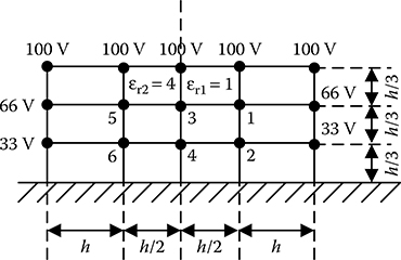
It is to be mentioned here that nodes 0, 2, 4, 5 and 6 lie on the dielectric interface. According to the boundary conditions on dielectric–dielectric interface, electric potential and tangential component of electric field remain constant on the dielectric interface. From Equation 14.33a and from Equation 14.33b From Equations 14.33c and 14.33d along the y-direction on the y–z plane, and from Equations 14.33e and 14.33f along the z-direction on the y–z plane, From Equation 14.32a, that is, Laplace’s equation that is valid for medium 1, and from Equation 14.32b, that is, Laplace’s equation that is valid for medium 2, Eliminating ∂V/∂x|0 from Equations 14.38 and 14.39, Equation 14.40 is the FDM equation for the unknown potential of a node lying on the dielectric interface in the 3D system with unequal nodal distances. For equal nodal distances in the 3D multi-dielectric system, that is, when s1 = s2 = s3 = s4 = s5 = s6 = 1, Equation 14.40 reduces to For a 2D multi-dielectric system with unequal nodal distances, the FDM equation for the unknown potential of a node lying on the dielectric interface will be as follows, where the dielectric interface is considered to be along the y-axis, as shown in Figure 14.11. For equal nodal distances in the 2D multi-dielectric system, that is, when s1 = s2 = s3 = s4 = 1, Equation 14.42 reduces to FIGURE 14.11 For the 3D arrangement with two different dielectric media, as shown in Figure 14.12, write the FDM equations for nodes 1, 2 and 3. The known node potentials are as follows: V13 = V23 = V33 = 100 V, V14 = V24 = V34 = 0 V, V11 = V21 = V31 = 50 V, V12 = V22 = V32 = 60 V and V15 = V35 = 55 V. Given that ε1 = 4 and ε2 = 1. Solution: In this problem, the largest nodal distance is h. FIGURE 14.12 For node 1: s1 = 0.5, s3 = 1, s2 = s4 = 0.333, s5 = 0.5 and s6 = 0.75. Therefore, as per Equation 14.8 Similarly for node 3: s1 = 0.5, s3 = 1, s2 = s4 = 0.333, s5 = 0.5 and s6 = 0.75. Therefore, as per Equation 14.8 For node 2, as per Equation 14.40, V1 = V3, V3 = V1,V2 = V23 = 100 V, V4 = V24 = 0 V, V5 = V21 = 50 V and V6 = V22 = 60 V and s1 = s3 = 0.333, s2 = 0.5, s4 = 0.75, s5 = 0.5, s6 = 1 and K = (ε1/ε2) = 4. For the 2D multi-dielectric configuration with series dielectric arrangement, as shown in Figure 14.13, write the FDM equations for the nodes having unknown potentials. Solution: For nodes 1, 2 and 3, symmetry of the configuration has to be considered with respect to the central plane. The nodal distances are equal for these three nodes. For node 1: For node 2: As per Equation 14.43, V1 = V1, V2 = V6, V3 = V3, V4 = V6 and K = (1/3). FIGURE 14.13 For node 3: For node 4: The nodal distances are unequal such that s1 = (1/3), s2 = 0.882 and s3 = s4 = 1 because the largest nodal distance is (3r/4). Then as per Equation 14.10 For node 5: The nodal distances are unequal such that s1 = (1/3), s2 = 1 and s3 = s4 = 1. Then as per Equation 14.10 For node 6: As per Equation 14.42, V1 = V5, V2 = V2, V3 = V7, V4 = 20 and K = (1/3). Nodal distance factors are s1 = s2 = s3 = 1 and s4 = (1/3). For node 7: The nodal distances are unequal such that s1 = (1/3) and s2 = s3 = s4 = 1. Then as per Equation 14.10 For the 2D multi-dielectric configuration with parallel dielectric arrangement, as shown in Figure 14.14, write the FDM equations for the nodes having unknown potentials. Solution: The largest nodal distance for this arrangement is h. Therefore, for node 1: s1 = 1, s2 = s4 = 0.333 and s3 = 0.5. Then as per Equation 14.10 For node 2: s1 = 1, s2 = s4 = 0.333 and s3 = 0.5. Then as per Equation 14.10 For node 3: As per Equation 14.42, V1 = V1, V2 = 100, V3 = V5, V4 = V4 and K = (1/4). Nodal distance factors are s1 = s3 = 0.5 and s2 = s4 = 0.333. For node 4: As per Equation 14.42, V1 = V2, V2 = V3, V3 = V6, V4 = 0 and K = (1/4). Nodal distance factors are s1 = s3 = 0.5 and s2 = s4 = 0.333. FIGURE 14.14 For node 5: s1 = 0.5, s2 = s4 = 0.333 and s3 = 1. Then as per Equation 14.10 For node 6: s1 = 0.5, s2 = s4 = 0.333 and s3 = 1. Then as per Equation 14.10
In this case, the dielectric interface is considered to be normal to the axis of symmetry. FDM equations need to be developed for a node lying on the dielectric interface. This node could be away from the axis of symmetry and could also be on the axis of symmetry. For the nodal arrangement shown in Figure 14.15, the z-component of electric flux density is the normal component on the dielectric interface that is parallel to the r-axis. where: Here, it is to be noted again that the potential function V is valid for medium 1 and V′ is valid for medium 2. FIGURE 14.15 Accordingly, two Laplace’s equations, one with V and the other with V′, need to be satisfied in this case, as given in Equations 14.45a and 14.45b. Equation 14.45a is valid for medium 1, and Equation 14.45b is valid for medium 2. Now, from the Taylor series expansion between the pair of nodes, the following expressions are obtained It is to be noted here that nodes 1, 0 and 3 lie on the dielectric interface. According to the boundary conditions on dielectric–dielectric interface, electric potential and tangential component of electric field remain constant on the dielectric interface. From Equations 14.46a and 14.46b along the r-direction on the dielectric interface, From Equations 14.46a and 14.46b considering the radial distance of the node 0 from the axis of symmetry to be sh, that is, r = sh, From Equation 14.46c and from Equation 14.46d From Equations 14.45a, 14.47, 14.48 and 14.49, and from Equations 14.45b, 14.47, 14.48 and 14.50, Eliminating ∂V/∂z|0 from Equations 14.51 and 14.52, Equation 14.53 is the FDM equation for the unknown potential of a node lying on the dielectric interface, where the node is away from the axis of symmetry, in an axi-symmetric system with unequal nodal distances having series dielectric arrangement (Figure 14.15). For equal nodal distances, that is, for s1 = s2 = s3 = s4 = 1, Equation 14.53 reduces to and for single-dielectric system, that is, for K = 1, with equal nodal distances Equation 14.54 reduces to Laplace’s equation in medium 1: Laplace’s equation in medium 2: As per Equation 14.44 where: FIGURE 14.16 Now, from the Taylor series expansion between the pair of nodes as shown in Figure 14.16, the following expressions are obtained: In Equation 14.58a, Hence, From Equation 14.58b, From Equation 14.58c, Therefore, from Laplace’s equation in medium 1, that is, Equation 14.56, and from Laplace’s equation in medium 2, that is, Equation 14.57, Eliminating ∂V/∂z|0 from Equations 14.60 and 14.61, Equation 14.62 is the FDM equation for the unknown potential of a node lying on the dielectric interface, where the node is on the axis of symmetry, in an axi-symmetric system with unequal nodal distances having series dielectric arrangement (Figure 14.16). For equal nodal distances, that is, for s1 = s2 = s4 = 1, Equation 14.62 reduces to and for a single-dielectric system, that is, for K = 1, with equal nodal distances Equation 14.63 reduces to In this case, the dielectric interface is considered to be parallel to the axis of symmetry. FDM equations need to be developed for a node lying on the dielectric interface. This node is away from the axis of symmetry, as in this case the dielectric interface cannot be on the axis of symmetry. For the nodal arrangement shown in Figure 14.17, the r-component of electric flux density is the normal component on the dielectric interface that is parallel to the z-axis. FIGURE 14.17 where: Now, from the Taylor series expansion between the pair of nodes, the expressions that may be obtained are as follows: From Equation 14.65a and from Equation 14.65b Again, from Equation 14.65a and from Equation 14.65b From Equations 14.65c and 14.65d along the z-direction on the dielectric interface, Satisfying Laplace’s equation in medium 1: Similarly, satisfying Laplace’s equation in medium 2: Eliminating ∂V/∂r|0 from Equations 14.71 and 14.72, Equation 14.73 is the FDM equation for unknown potential of a node lying on the dielectric interface, where the node is away from the axis of symmetry, in an axi-symmetric system with unequal nodal distances having a parallel dielectric arrangement. For equal nodal distances, that is, when s1 = s2 = s3 = s4 = 1, Equation 14.73 reduces to and for a single-dielectric system, that is, K = 1, with equal nodal distances Equation 14.74 reduces to For the axi-symmetric multi-dielectric configuration with series dielectric arrangement, as shown in Figure 14.18, write the FDM equations for the nodes having unknown potentials. Solution: In this configuration, the largest nodal distance is (2r/3). Therefore, the respective nodal distance factors are calculated based on this largest nodal distance. For node 1: As per Equation 14.29, V1 = V5, V2 = 100, V4 = V2, s1 = 0.5 and s2 = s4 = 1. For node 2: As per Equation 14.62, V1 = V6, V2 = V1, V4 = V3, s1 = 0.5, s2 = s4 = 1 and K = (1/4). For node 3: As per Equation 14.29, V1 = V7, V2 = V2, V4 = 0, s1 = 0.5 and s2 = s4 = 1. FIGURE 14.18 For node 4: The nodal distances are unequal such that s1 = 1, s2 = 0.086, s3 = 0.5, s4 = 1 and s = 0.5; V1 = 65, V2 = 100, V3 = 100 and V4 = V5. Then as per Equation 14.23 For node 5: The nodal distances are unequal such that s1 = s2 = s4 = 1, s3 = 0.5 and s = 0.5; V1 = 32, V2 = V4, V3 = V1 and V4 = V6. Then as per Equation 14.23 For node 6: As per Equation 14.53, V1 = 15, V2 = V5, V3 = V2, V4 = V7, s1 = s2 = s4 = 1, s3 = 0.5, s = 0.5 and K = (1/4).
For node 7: The nodal distances are unequal such that s1 = s2 = s4 = 1, s3 = 0.5 and s = 0.5; V1 = 5, V2 = V6, V3 = V3 and V4 = 0. Then as per Equation 14.23 For the axi-symmetric multi-dielectric configuration with parallel dielectric arrangement, as shown in Figure 14.19, write the FDM equations for the nodes having unknown potentials. Solution: In this configuration the largest nodal distance is h. Therefore, the respective nodal distance factors are calculated based on this largest nodal distance. For node 1: The nodal distances are unequal such that s1 = s2 = s4 = 1, s3 = 0.5 and s = 1.833; V1 = 60, V2 = 100, V3 = V3 and V4 = V2. Then as per Equation 14.23 FIGURE 14.19
For node 2: The nodal distances are unequal such that s1 = s2 = s4 = 1, s3 = 0.5 and s = 1.833; V1 = 25, V2 = V1, V3 = V4 and V4 = 0. Then as per Equation 14.23 For node 3: The nodal distances are unequal such that s1 = 0.5, s2 = s4 = 1, s3 = 0.333 and s = 1.333; V1 = V1, V2 = 100, V3 = V5, V4 = V4 and K = (1/2). Then as per Equation 14.73 For node 4: The nodal distances are unequal such that s1 = 0.5, s2 = s4 = 1, s3 = 0.333 and s = 1.333; V1 = V2, V2 = V3, V3 = V6, V4 = 0 and K = (1/2). Then as per Equation 14.73 For node 5: The nodal distances are unequal such that s2 = s3 = s4 = 1, s1 = 0.333 and s = 1; V1 = V3, V2 = 100, V3 = 66 and V4 = V6. Then as per Equation 14.23
For node 6: The nodal distances are unequal such that s2 = s3 = s4 = 1, s1 = 0.333 and s = 1; V1 = V4, V2 = V5, V3 = 33 and V4 = 0. Then as per Equation 14.23
In FDM, for the 2D system, the entire ROI, that is, the region where the field distribution is required to be calculated, is discretized using either rectangles or squares. In the 3D system, discretization is done using either rectangular parallelepipeds or cubes. Because the potential is commonly assumed to vary linearly between two successive nodes, the nodes need to be closely spaced where the field varies significantly in space. This is generally the case near the electrodes or dielectric boundaries, particularly in the cases of contours having sharp corners. On the other hand, in the region away from the electrodes or dielectric boundaries, where the field does not change rapidly in space, the nodes may be spaced relatively widely apart. For multi-dielectric problems, care should be taken during discretization to make sure that only one dielectric is present between two consecutive nodes. This is achieved by arranging one layer of nodes along the dielectric–dielectric interface. The finite difference model of a problem gives a point-wise approximation to the governing equations, for example, Laplace’s equation. This model is formed by writing difference equations for an array of grid points called nodes, which is improved as more nodes are used in the simulation. With the help of FDM, one can treat some fairly difficult problems; but for problems having irregular geometries or an unusual specification of boundary conditions, the FDM becomes hard to use. As an example of how FDM might be used to represent a complex geometrical shape, consider the high-voltage insulator cross section shown in Figure 14.20. A finite difference mesh would reasonably cover the insulator volume, but the boundaries must be approximated by a series of horizontal and vertical lines or stair steps. This results in poor approximation of the curved insulator boundary. FIGURE 14.20 FDM is well suited for simulating bounded field regions, that is, field regions having well-defined boundaries. For unbounded field regions, a major difficulty in the implementation of FDM is the placement of nodes in the space, which is far away from the components that affect the field distribution. This difficulty is surmounted by placing a fictitious boundary, as shown in Figure 14.21, at a location relatively distant from the components influencing the field. This fictitious boundary is placed with the assumption that the pair of nodes on both sides of this boundary has same potential, for example, the potential of the nodes 1, 3, 5 and 7 are assumed to be same as that of the nodes 2, 4, 6 and 8, respectively. If this fictitious boundary is placed in a region where the field does not vary rapidly in space, then the imposition of this fictitious boundary does not incorporate any significant error in the field computation. The accuracy of simulation is dependent on the nature of discretization of the field region and hence it is important to determine the simulation accuracy using certain well-accepted criteria as detailed below. The potential error on the electrode boundaries can be determined at a number of checkpoints on the electrode surface between two consecutive nodes. Such check points are often called control points. This potential error is defined as the difference between the known potential of the electrode and the computed potential at the control point. From such calculations one can determine the average or the maximum or the mean squared value of the potential error. FIGURE 14.21 The error in the electric field intensity is usually higher than the potential error. Hence, compared to the potential error the deviation angle on the electrode surface is a more sensitive indicator of the simulation accuracy. The deviation angle is defined as the angular deviation of the electric stress vector at the control point on the electrode surface from the direction of the normal to its surface. In multi-dielectric systems, the discrepancy in the tangential electric stress at the control points on the dielectric interface can be computed. Another criterion for checking the simulation accuracy is to compute the discrepancy in the normal flux density at the control point on the dielectric interface. For a good simulation, such discrepancies should be small. In FDM, the potential of any node is related to either four connected nodes in the 2D system or six connected nodes in the 3D system. Hence, if a field region is discretized using N (N >> 1) number of nodes, then the system of FDM equation will be an N × N matrix. But in each row of this matrix, there will be non-zero value in only five or seven elements depending on the dimension of the simulated system and all the other elements out of N elements of each row of the matrix will be zero. Hence, it is obvious that the system of FDM equations generates a highly sparse matrix. Hence, it is advisable to solve the system of FDM equations by an iterative technique such as Gauss–Seidel method rather than using a direct method such as Gaussian elimination. In the iterative methods, suitable technique is to be employed to achieve accelerated convergence.
FIGURE 14.22 Length of the transmission line conductors can be considered to be very large compared to the diameter of the conductors as well as the conductor spacings. Hence, the field due to three-phase transmission line conductors could be computed as a 2D case, as the field is assumed to be not varying along the length of the conductors. Figure 14.22 shows a typical arrangement of three-phase transmission line conductors, where the line conductors are arranged in an equilateral triangle formation. The length of the line conductor is taken in the direction perpendicular to the plane of the paper. The field is assumed to be computed at the mid-span, so that the earth surface and the transmission towers are considered to be far away from the conductors. This is an example of unbounded field region problem and hence fictitious boundaries, as discussed in Section 14.6.2, need to be introduced, as shown in Figure 14.22. FDM grid, as shown in Figure 14.22, depicts smaller nodal distances where the field is expected to be higher, whereas the nodal distances are higher elsewhere. This example involves only one dielectric as the conductors are surrounded by air. It should be stressed here that all the FDM grids shown in section 14.7 are suggestive only. Users may use other grids using their discretion. Figure 14.23 shows the FDM grid for a simple post-type insulator stressed between two electrodes. It is an axi-symmetric system with two dielectric media. It is also an example of unbounded field region problem and hence a fictitious boundary on the right has been introduced, as shown in Figure 14.23. There should be two more fictitious boundaries that need to be introduced, one at the top and one at the bottom. But it is left to the imagination of the reader. Coarse and finer meshes are taken depending on the nature of field concentration. Typically finer mesh size is to be taken near the boundaries and as one goes away from the boundary relatively higher mesh size could be taken without compromising accuracy. FIGURE 14.23 Disc-type insulators are widely used for supporting high-voltage transmission line conductors from the tower cross-arm. A realistic disc-type insulator and the associated FDM grid are shown in Figure 14.24. It is an axi-symmetric case study with two dielectric media, typically porcelain (εr1) as solid insulating material surrounded by air (εr2). As it is an unbounded field region problem, three fictitious boundaries have been introduced for field computation, as shown in Figure 14.24. As stated in the earlier examples, the nodal distances are to be suitably chosen in relation to field distribution, so that high accuracy is achieved. Contrary to post-type insulators, the high-voltage end of the disc-type insulator is at the bottom (the pin, as shown in Figure 14.24) and the earthed end is at the top (the cap, as shown in Figure 14.24). FIGURE 14.24
1. Finite difference method is based on a. Differential equation technique b. Integral equation technique c. Monte Carlo technique d. Experimental technique 2. FDM equations may be derived from a. Logarithmic series expansion b. Binomial series expansion c. Taylor series expansion d. Fourier series expansion 3. FDM is best suited to solve numerically a. Laplace’s equation b. Poisson’s equation c. Gauss’s law in differential form d. Both (a) and (b) 4. For equally spaced nodes in a 2D system, FDM equation is given by a. V0 = (V1 + V2 + V3 + V4 + V0)/5 b. V0 = (V1 + V2 + V3 + V4 + V0)/4 c. V0 = (2V1 + V2 + V3 + V4)/4 d. V0 = (V1 + V2 + V3 + V4)/4 5. Between any two connected nodes in FDM, electric field intensity is commonly assumed to be a. Linearly varying b. Constant c. Inversely varying d. Exponentially varying 6. FDM equations are most commonly solved by a. Iterative technique b. Gaussian elimination c. LU decomposition d. Both (b) and (c) 7. For equally spaced nodes in a 3D system, FDM equation is given by a. V0 = (V1 + V2 + V3 + V4)/4 b. V0 = (V1 + V2 + V3 + V4 + V5 + V6)/6 c. V0 = (V1 + V2 + V3 + V4 + V5 + V6)/4 d. V0 = (V1 + V2 + V3 + V4)/6 8. Matrix representation of the system of equations to be solved in FDM gives a. Diagonal matrix b. Unit matrix c. Sparse matrix d. Nearly full matrix 9. The FDM equation V0 = (V1 + V2 + V3 + V4)/4 + (V1 − V3)/8s is valid for a. 2D system with equal nodal distances b. 2D system with unequal nodal distances c. Axi-symmetric system with equal nodal distances d. Axi-symmetric system with unequal nodal distances 10. Simulation of unbounded configurations extended up to infinity gives rise to difficulties in a. Finite difference method b. Finite element method c. Charge simulation method d. Both (a) and (b) 11. The nodal FDM equation V0 = (4V1 + V2 + V4)/6 for equally spaced nodes is valid for a node a. In a 2D system b. In a 3D system c. On the axis in an axi-symmetric system d. On dielectric boundary in a 2D system 12. For a given configuration in FDM, if the number of nodes is increased, then accuracy a. Remains unchanged b. Decreases c. Increases d. Oscillates 13. In simulation of multi-dielectric problem by FDM, two successive nodes are placed in such a way that a. Both lie in the same dielectric b. Each one lies in different dielectric c. One on the boundary and other one in a dielectric d. Both (a) and (c) 14. On the conductor boundary, simulation accuracy is checked by calculating a. Potential error b. Continuity of normal component of electric flux density c. Deviation angle d. Both (a) and (c) 15. For a given 2D configuration in FDM, if the inter-node spacing of equally spaced nodes is increased, then the results a. Get better b. Get worse c. Remain unchanged d. Oscillate 16. On the dielectric–dielectric interface, simulation accuracy is checked by calculating a. Potential error b. Continuity of normal component of electric flux density c. Deviation angle d. Both (a) and (c) 17. To achieve higher simulation accuracy as well as faster computation, discretization of the field region should be done in such a way that a. The nodes are closely spaced everywhere b. The nodes are sparsely spaced everywhere c. The nodes are closely spaced where the field varies sharply and are sparsely spaced elsewhere d. The nodes are sparsely spaced where the field varies sharply and are closely spaced elsewhere 18. In general, the nodes need to be spaced unequally a. Near the electrode boundaries b. Near the dielectric–dielectric boundaries c. Far away from the boundaries d. Both (a) and (b) 1) a; 2) c; 3) a; 4) d; 5) b; 6) a; 7) b; 8) c; 9) c; 10) d; 11) c; 12) c; 13) d; 14) d; 15) b; 16) b; 17) c; 18) d14.1 Introduction
14.2 FDM Equations in 3D System for Single-Dielectric Medium

Unequal nodal distances for FDM equation development in three-dimensional (3D) system.
Unequal nodal distances for FDM equation development in 2D system.PROBLEM 14.1
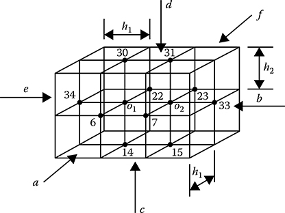
3D arrangement with two nodes having unknown potentials.PROBLEM 14.2

2D arrangement with nodes having unknown potentials.14.3 FDM Equations in Axi-Symmetric System for Single-Dielectric Medium

Typical axi-symmetric insulator geometry.14.3.1 FDM Equation for a Node Lying Away from the Axis of Symmetry
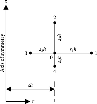
Unequal nodal distances for FDM equation development in axi-symmetric system for a node lying away from the axis of symmetry.14.3.2 FDM Equation for a Node Lying on the Axis of Symmetry

Axi-symmetric system with unequal nodal distances with a node lying on the axis of symmetry.PROBLEM 14.3

Nodal arrangement pertaining to Problem 14.3.PROBLEM 14.4

Nodal arrangement pertaining to Problem 14.4.14.4 FDM Equations in 3D System for Multi-Dielectric Media

Nodal arrangement for FDM equation development in 3D system with multi-dielectric media.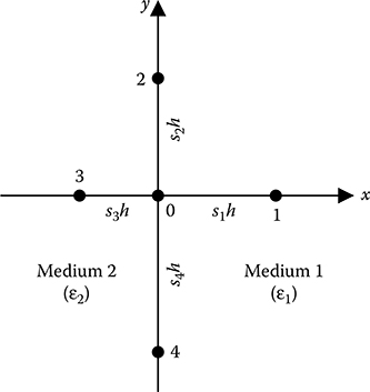
Nodal arrangement for FDM equation development in 2D system with multi-dielectric media.PROBLEM 14.5

(See colour insert.) Nodal arrangement pertaining to Problem 14.5.PROBLEM 14.6

Nodal arrangement pertaining to Problem 14.6.PROBLEM 14.7
Nodal arrangement pertaining to Problem 14.7.14.5 FDM Equations in Axi-Symmetric System for Multi-Dielectric Media
14.5.1 For Series Dielectric Media
14.5.1.1 For the Node on the Dielectric Interface Lying Away from the Axis of Symmetry

Nodal arrangement for FDM equation development in axi-symmetric system with multi-dielectric media in series dielectric arrangement when the node is lying away from the axis of symmetry.14.5.1.2 For the Node on the Dielectric Interface Lying on the Axis of Symmetry

Nodal arrangement for FDM equation development in axi-symmetric system with multi-dielectric media in series dielectric arrangement when the node is lying on the axis of symmetry.14.5.2 For Parallel Dielectric Media

Nodal arrangement for FDM equation development in axi-symmetric system with multi-dielectric media in parallel dielectric arrangement when the node is lying away from the axis of symmetry.PROBLEM 14.8

Nodal arrangement pertaining to Problem 14.8.PROBLEM 14.9

Nodal arrangement pertaining to Problem 14.9.14.6 Simulation Details
14.6.1 Discretization

Discretization of insulator geometry by FDM mesh.14.6.2 Simulation of an Unbounded Field Region
14.6.3 Accuracy Criteria
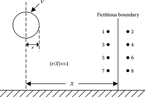
Simulation of unbounded field region.14.6.4 System of FDM Equation
14.7 FDM Examples
14.7.1 Transmission Line Parallel Conductors

FDM grid for three-phase transmission line conductors.14.7.2 Post-Type Insulator

FDM grid for a simple post-type insulator.14.7.3 Disc-Type Insulator

FDM grid for a disc-type insulator.Objective Type Questions
Answers:
Bibliography
1. G. Shortley, R. Weller, P. Darby and E.H. Gamble, ‘Numerical solution of axisymmetrical problems with applications to electrostatics and torsion’, Journal of Applied Physics, Vol. 18, pp. 116–129, 1947.
2. D.N. De G. Allen and S.C.R. Dennis, ‘The application of relaxation methods to the solution of differential equations in three dimensions’, Quarterly Journal of Mechanics Applied Mathematics, Vol. 4, pp. 199–208, 1951.
3. H.E. Kulsrud, ‘A practical technique for the determination of the optimum relaxation factor of successive over-relaxation method’, Communication Association for Computing Machinery, Vol. 4, pp. 184–187, 1961.
4. B.A. Carré, ‘The determination of the optimum accelerating factor for successive over-relaxation’, Computer Journal, Vol. 4, pp. 73–78, 1961.
5. K.J. Binns and P.J. Lawrenson, Analysis and Computation of Electric and Magnetic Field Problems, Pergamon Press, Oxford, 1963.
6. G.E. Forsythe and W.R. Wasow, Finite Difference Methods for Partial Differential Equations, Wiley, New York, 1965.
7. D.F. Binns, ‘Calculation of field factor for a vertical sphere gap taking account of surrounding earthed surfaces’, Proceedings of IEEE, Vol. 112, pp. 1575–1582, 1965.
8. M.V. Schneider, ‘Computation of impedance and attenuation of TEM-lines by finite difference methods’, IEEE Transactions on Microwave Theory and Techniques, Vol. 13, pp. 793–800, 1965.
9. M.J. Billings, B.P. Nellist and P. Swarbrick, ‘Investigation into new designs for h.v. insulators using synthetic materials’, Proceedings of IEEE, Vol. 113, No. 10, pp. 1643–1648, 1966.
10. R.H. Galloway, H.McL. Ryan and M.F. Scott, ‘Calculation of electric fields by digital computer’, Proceedings of IEEE, Vol. 114, No.6, pp. 824–829, 1967.
11. J.T. Storey and M.J. Billings, ‘General digital-computer program for the determination of 3-dimensional electrostatic axially symmetric fields’, Proceedings of IEEE, Vol. 114, No. 10, pp. 1551–1555, 1967.
12. J.W. Duncan, ‘The accuracy of finite-difference solutions of Laplace’s equation’, IEEE Transactions on Microwave Theory and Techniques, Vol. 15, No. 10, pp. 575–582, 1967.
13. J.T. Storey and M.J. Billings, ‘Determination of the 3-dimensional electrostatic field in a curved bushing’, Proceedings of IEEE, Vol. 116, No. 4, pp. 639–643, 1969.
14. J.T. Storey, ‘The determination of axially symmetric fields by digital computation’, IEEE Transactions on Electrical Insulation, Vol. 4, No. 2, pp. 23–30, 1969.
15. M.F. Scott, J.M. Mattingley, M. John and H.M. Ryan, ‘Computation of electric fields: Recent developments and practical applications’, IEEE Transactions on Electrical Insulation, Vol. 9, No. 1, pp. 18–25, 1974.
16. B. Aldefeld, ‘Computer-aided design of electromagnetic actuators using finite difference techniques’, IEEE Transactions on Magnetics, Vol. 12, No. 6, p. 1047, 1976.
17. B. Tomescu and F.M. Tomescu, ‘Electrostatic field computation in non-rectangular configurations’, Revue Roumaine des Science Techniques Series Electrotechnique et Energetique, Vol. 22, No. 4, pp. 491–498, 1977.
18. G. Molinari, M.R. Podesta, G. Sciutto and A. Viviani, ‘Finite difference method with irregular grid and transformed discretization metric’, IEEE PES Winter Meeting, New York, January 29–February 3, 1978.
19. E.S. Kolechitskii, A.A. Filippov and O.V. Firsova, ‘Methods for calculating electric fields of high-voltage equipment’, Soviet Electrical Engineering, Vol. 51, No. 4, pp. 17–22, 1980.
20. E.F. Fuch and K. Senske, ‘Comparison of iterative solutions of the finite difference method with measurements as applied to Poisson’s and the diffusion equations’, IEEE PES Winter Meeting, Atlanta, GA, February 1–6, 1981.
21. F. Donazzi and G. Luoni, ‘Comparison of different methods in computing electrostatic fields’, IEEE Transactions on Magnetics, Vol. 19, No. 6, pp. 2596–2599, 1983.
22. M. Hizal, ‘Computation of the electric field at a solid/gas interface in the presence of surface and volume charges’, IEEE Proceedings A, Vol. 133, No. 9, pp. 577–586, 1986.
23. A. Christ and H. Hartnagel, ‘Three-dimensional finite-difference method for the analysis of microwave device embedding’, IEEE Transactions on MTT, Vol. 35, pp. 688–696, 1987.
24. A.A. Read and D.T. Stephenson, ‘Computers and computer graphics in teaching electromagnetic fields’, Proceedings of Frontiers in Education Conference, IEEE Publication, Terre Haute, IN, pp. 523–530, October 24–27, 1987.
25. M.J. Sablik, D. Golimowski, J.R. Sharber and J.D. Winningham, ‘Computer simulation of a 360° field-of-view top-hat electrostatic analyser’, Review of Scientific Instruments, Vol. 59, No. 1, pp. 146–155, 1988.
26. M. Abdel-Salam and M.T. El-Mohandes, ‘Combined method based on finite differences and charge simulation for calculating electric fields’, IEEE Transactions on Industry Applications, Vol. 25, No. 6, pp. 1060–1066, 1989.
27. D. Hollmann, S. Haffa and W. Wiesbeck, ‘Improved analysis of dielectric resonator coupling using a three-dimensional finite difference method’, Proceedings of 21st European Microwave Conference, Stuttgart, Germany, Vol. 1, pp. 565–570, September 9–12, Microwave Exhibitions and Publishers, Richmond, UK, 1991.
28. N. Femia and V. Tucci, ‘Computer models of electrical discharges’, Proceedings of International Conference on Computation in Electromagnetics, London, IEE Conference Publication No. 350, pp. 119–122, November 25–27, 1991.
29. R.K. Gordon, M.D. Tew and A.Z. Elsherbeni, ‘An efficient finite difference method for finding the electric potential in regions with small perturbations’, Proceedings of IEEE Antennas and Propagation Society International Symposium, Chicago, IL, June 18–25, IEEE Publication, New Jersey, 1992.
30. A. Bouziane, K. Hidaka, J.E. Jones, A.R. Rowlands, M.C. Tapiamacioglu and R.T. Waters, ‘Paraxial corona discharge. II. Simulation and analysis’, IEE Proceedings – Science, Measurement and Technology, Vol. 141, No. 3, pp. 205–214, 1994.
31. O. Sucre and D. Suster, ‘Solution of unbounded bi-dimensional boundary-value problems with the finite-difference method’, Proceedings of the International Congress on Numerical Methods in Engineering and Applied Sciences, CIMENICS, Mérida, Venezuela, pp. 231–238, March, Venezuelan Society of Numerical Methods in Engineering, Caracas, Venezuela, 1996.
32. E. Lami, F. Mattachini, R. Sala and H. Vigl, ‘A mathematical model of electrostatic field in wires-plate electrostatic precipitators’, Journal of Electrostatics, Vol. 39, No. 1, pp. 1–21, 1997.
33. L. Li and E. Wang, ‘An improved finite difference method for calculating electric field in high voltage vacuum interrupter’, Proceedings of 20th International Symposium on Discharges and Electrical Insulation in Vacuum, Tours, France, pp. 519–522, July 1–5, IEEE Publication, 2002.
34. M.A. Elhirbawy, L.S. Jennings, S.M. Al Dhalaan and W.W.L. Keerthipala, ‘Practical results and finite difference method to analyze the electric and magnetic field coupling between power transmission line and pipeline’, Proceedings of the 2003 International Symposium on Circuits and Systems, Bangkok, Thailand, Vol. 3, pp. 431–438, May 25–28, IEEE Publication, 2003.