
19
Electric Field Optimization
ABSTRACT The electricity supply system nowadays is characterized by two aspects: (1) high voltages at both transmission and distribution levels and (2) distribution of electric power in densely populated areas. Electric field distribution and the design of insulation system is affected by both these aspects. The higher voltage levels cause higher stresses in the insulation system, whereas the supply of power to populated regions demands compactness of the power equipment, which in turn increases the stresses within the insulation system of the equipment. Critical domains of high-voltage arrangement, which will have high field concentrations, cannot be designed by simple bodies such as spheres, rings or cylinders, which are easier to manufacture. Optimization methods are applied to high-voltage system so as to design electrodes as well as insulator contours in such a way that prescribed field distributions on defined surfaces in the critical domain are obtained. Consequently, such methodologies help to use the field space optimally within high-voltage system. This chapter presents a review of the works done in the area of optimization of high-voltage field and then discusses a few specific application examples that involve classical optimization techniques as well as techniques based on artificial neural network (ANN) and evolutionary algorithms.
19.1 Introduction
An important objective in insulating system design is to obtain electrodes and insulator contours, which will withstand all the electrical stresses that may appear during normal operation as well as during occasional transient events. For safe and reliable operation of any high-voltage equipment, the maximum values of electric field stresses in the insulating system must be lower, or at the most equal, to the allowable values. From this viewpoint, the optimal insulating system element contours are those on which the uniformly distributed field stresses or the desired distribution of field stresses remain within the allowable limit.
In the classical approach to insulating system design, system elements with simple geometrical forms such as sphere, ring, cylinder and so on were used and electric field strength was controlled by varying the distances between the system elements. This approach although works in practice but results in non-uniform electric field distribution, leading to suboptimal utilization of the capability of insulation system. The present-day need for better space utilization in the case of high-voltage supply system demands application of electrode and insulator contour optimization in insulating system design. The contours obtained through optimization processes have either uniformly distributed field intensity or a desired distribution of field intensity, which is achievable because of their not so simple geometric shapes. From another viewpoint, an efficient approach to electrode and insulator design is to have optimized profile(s) of electrode and/or insulator such that the dimensions are minimum for a given voltage rating, thus minimizing the space needed for and also the cost of installation.
The criterion most commonly used for the optimization of electrode contour is the minimization of the normal component of the electric field intensity on the surface of the electrodes, as it increases the discharge initiation voltage. On the other hand, the minimization of the tangential component of the electric field intensity along the surface is the preferred criterion for insulator contour optimization, as it increases the onset voltage of surface flashover. However, the minimization of the resultant field intensity on the insulator surface is also used as criterion for insulator contour optimization.
19.2 Review of Published Works
From a mathematical viewpoint, as early as in 1915, it was reported by Spielrein [1] that the change in the field on the surface of a given electrode can be obtained by a change in the curvature of the contour as given below:
where:
κ is the total curvature of the electrode surface at any arbitrary point
Equation 19.1 shows the relationship between the electric field intensity, decrease in electric field intensity due to a displacement normal to the contour and the total curvature of the contour at any arbitrary point on the contour. Thus, the change of curvature necessary to achieve the desired change in field can be deduced from Equation 19.1. This change in curvature (Δκ) at every contour point, in accordance with the deviation of electric field intensity (ΔE) from the desired field strength, can be calculated as follows:
In order to maintain the proportional relationship between the deviation of electric field intensity and the required change in curvature, small differences are to be assumed. The optimization procedure for electrodes must alter the contour in such a way that at any contour point the electric field intensity equals the desired value of field intensity, which is below the value required for discharge initiation with a safety margin.
Determination of the right shape for the boundary part of a plane sparking gap based on the theory of conformal mapping was reported by Rogowski [2] in 1923. Later in 1950, Félici [3] reported the use of conformal mapping for designing capacitor plate to have an electric field of constant strength.
19.2.1 Conventional Contour Correction Techniques for Electrode and Insulator Optimization
In 1975, Singer and Grafoner [4] published a methodology for optimizing electrodes and insulators designed for practical use. In their method, domains with constant field intensity were obtained for axi-symmetric arrangements by displacing contour points successively. Some more conventional methods of electric field optimization were reported in References [5–7].
In 1982, Misaki et al. [8] reported a method to get the optimum design of epoxy pole spacers used in sulphur hexafluoride (SF6) gas-insulated cables. In their method an improved surface charge method using curved surface elements was employed for the computation of three-dimensional (3D) electric field distribution and the results of electric field computation were used for the optimization of insulator design. The optimum insulator design was performed automatically by correcting the insulator contour using a simple vector computation. In this method, the insulator contour was corrected in such a way that both tangential field intensity and normal field intensity became uniform along the new contour. If the insulator contour moves in the direction of the normal vector, then the tangential field intensity decreases, and if the insulator contour moves in the direction opposite to that of the normal vector, then the normal field intensity decreases on the insulator surface. Therefore, the direction in which correction of the insulator contour had to be carried out was decided by taking note of the normal stress on the insulator surface. The insulator contour was corrected in proportion to the normal Maxwell’s stress, which was obtained from both tangential and normal field intensities. A method for 3D electrode contour optimization was reported by Misaki et al. [9] in 1983, in which the electric field intensity and force on the electrode surface were computed, and then the electrode contour was moved in the opposite direction of the force and the contour displacement was done in proportion to the magnitude of the force.
In 1983, Grönewald [10] described an algorithm based on the computer-aided design (CAD) concept for optimizing electrode contour to obtain a given field distribution on the surface. They proposed a two-step procedure that strictly separated electric field calculation and geometrical contour corrections. At any point on the contour, the changes in curvature depending on the desired field were described with the help of relationships developed between field quantity and geometry. The new contour was found by a simultaneous displacement of all discretizing points on the contour.
Stih [11] in his paper described an iterative procedure for designing optimally stressed insulating system. The described procedure combined the approach of varying the distances between system elements and optimizing their contours. Axially symmetric electric fields were computed by an integral equation technique introducing cubic spline expansion for charge density distribution function. In an extension of the contour correction techniques reported in References [4,8,9], an additional step was introduced in this work in the form of smooth approximation of the corrected contour by circular arcs, which enabled relatively simple geometrical description of the optimal contours.
Abdel-Salam and Stanek [12,13] reported a method for optimizing the field stress on high-voltage insulators through the modification of their profile to obtain a uniform distribution of the tangential field along the insulator surface. An algorithm based on a modified charge simulation technique was developed for calculating the tangential field component along the insulator surface. After computation of the tangential field distribution for the non-optimized profile, the insulator profile was enlarged or reduced on going up or down along its axis. If the field distribution increased, when moving along the axis of the insulator, the profile radius was increased in that direction and if the field distribution decreased, then the profile radius was decreased. Exponential mathematical expressions, which defined a smooth enlargement/reduction of the profile radius, were used in this work.
Mosch et al. [14] published a method of optimization of large electrodes of ultra high voltage (UHV) testing equipment designed on the basis of inception of streamer and leader discharges. The stochastic nature of these two discharge processes leads to the well-known area effects, and also to time effects. Hence, the proposed model was related to the volume–time concept. The design procedure started with choosing the principle of field control and the main geometric parameters of the electrode. Then the electric field was calculated numerically and from the results of electric field computation the inception voltages ViS, for streamer discharge, and ViL, for leader discharge, were determined. The calculated values were compared to the maximum output voltage. If the calculated values were less, then the geometry of the electrode was improved and the cycle of computation was repeated till an optimum design was achieved. A similar study was reported by Kato et al. in Reference [15]. In this paper, they described a technique for the optimization of high-voltage electrode contour to make the electrical insulation performance highest by introducing the volume–time characteristics into the optimization procedure. Optimization technique was also investigated from the viewpoints of computation efficiency and accuracy.
The basic principle of electrode optimization method suggested by Liu and Sheng [16] was that the electrode was divided into two parts: the fixed part and the part to be optimized. The fixed part was simulated by the simulation charges and the second part by the optimization charges, in which the magnitudes and coordinates were assigned first. Normally, the magnitudes of the optimization charges were taken as optimization variables. In this method, the coordinates instead of the magnitudes of optimization charges were taken as the optimization variables. The reported results of optimization examples indicated that the use of the proposed method yielded good results. Liu et al. [17] also described an automatic procedure for the optimization of axi-symmetric electrodes using boundary element method. The criterion employed for the optimization of the shape of the electrodes was the minimization of the maximum field intensity on the surface of the electrodes. The proposed method was applicable in 3D fields too. Judge and Lopez-Roldan in Reference [18] discussed an approach to design components for high-voltage engineering based on the boundary element method in two and three dimensions. Optimization of the components was performed using an iterative method of refining a design and re-analyzing without having to resort to repeated prototype building and testing. Studies on the optimization of electrode contours using circular contour elements [19] and optimization of multi-electrode system [20] have also been reported in the literature.
Däumling and Singer [21] described a new algorithm based on the CAD concept for the optimization of insulator contours to get a given field distribution along the surface. Three optimization procedures with different targets were investigated: (1) uniform tangential field strength, (2) uniform resultant field strength and (3) uniform electrostatic pressure along the insulator contour. It was found that achieving a low tangential field strength component was not sufficient, and it was necessary to reduce the maximum value of the resultant field strength as far as possible, especially in the case of high air humidity.
Caminhas et al. [22] determined the optimum profile and location of shielding electrode used in high-voltage equipment with the aim to obtain a linear voltage distribution along the axis of symmetry. It was shown that the combined usage of the charge simulation method and the Broyden–Fletcher–Goldfarb–Shannon optimization technique was both efficient and simple. Very good attempt was made to review various optimization methods applicable to the specific case.
19.2.2 Optimization of High-Voltage System Elements
Optimization of field stresses in high-voltage bushings have been reported in References [23,24] and special techniques for electrode and insulator contour optimization, which were claimed to be efficient, have been reported in References [25–27]. Efficient techniques for electric field optimization using personal computers were reported in References [28,29]. Studies on 3D electric field optimization in high-voltage equipment was reported by Trinitis [30,31]. In Reference [31] optimal electric field strength distribution for 3D problems was achieved by utilizing a parametric CAD modelling system coupled to a 3D electric field calculation program. These two components were then linked to a numerical optimization algorithm. The package comprising the above-mentioned three components was then able to automatically optimize arbitrary 3D field problems in high-voltage engineering. Optimization of high-voltage insulators in 3D field configurations was reported in Reference [32].
High gradient insulators (HGI) consist of a periodic array of insulator and metal rings, which have been found to be more resilient to vacuum surface breakdown than homogeneous insulators of the same length. Studies based on calculations and experiments were reported by Leopold et al. [33] to understand the effect of geometry on the performance of well conditioned, flat surface HGI assemblies.
19.2.3 Soft-Computing Techniques for Electrode and Insulator Optimization
With the advent of artificial intelligence, it was realized that instead of iterative calculation of electric field and contour modification, electric field optimization could be done based on artificial neural network (ANN). Once the ANN is trained, optimum solution satisfying desired specification can be found without iterative calculation, resulting in high-speed method. ANN with supervised learning by error back-propagation method as used for high-voltage electrode optimization was reported by Chakravorti and Mukherjee [34]. It was found that the trained ANN can give results with mean absolute error (MAE) of about 1% in comparison with analytically obtained results. For electrode contour optimization, the results of electric field calculations for some pre-determined contours of an axi-symmetric electrode arrangement were used for training the ANN. Then the trained ANN was used to give the optimized electrode contour to obtain a desired field strength distribution on the electrode surface. Similar study on application of ANN in the design of toroidal electrodes was reported by Bhattacharya et al. [35]. Optimization of HV electrode systems by ANN with resilient propagation was carried out by Mukherjee et al. [36]. Two axi-symmetric examples were optimized: (1) the first one was the termination of a single-phase gas-insulated substation (GIS) bus and (2) the second one was a shield ring in a three-phase transformer. Charge simulation method was used for preparation of the training sets as well as for checking the test outputs from the ANN. The procedure of the electric field optimization method based on ANN as reported by Okubo et al. [37] comprised two ANNs. As the electric field strength on a high-voltage electrode surface has empirical relationship with the curvature and the gap length, one ANN, called ‘NN1’, was trained to learn this relationship. Another ANN, called ‘NN2’, was trained to learn the relationship between a set of curvature, gap length and electrode contour. Once the learning of the two ANNs were completed, the curvature, gap length and electrode contour for the optimized electrode configuration were obtained as output by giving the target electric field distribution as input into the trained ANN system.
In Reference [38], ANN-based studies have been presented for the optimization of insulator contour in multiple dielectric systems, where the degree of field nonlinearity is more than that for single-dielectric configurations. ANN-aided contour optimization of axi-symmetric insulators in multi-dielectric arrangements had been carried out to obtain not only a uniform but also a complex electric stress distribution along the insulator surface. Multilayer feed-forward networks with error-back propagation as well as resilient propagation learning algorithms were employed.
As each ANN application requires a certain amount of training to achieve the desired accuracy, Chatterjee et al. [39] in their paper discussed the development of a self-organizing fuzzy inference system for designing optimized electrode contours. The process of optimization was accelerated using a fuzzy inference system that eliminated training time. Reliability of the proposed methodology was further improved by implementing an algorithm for automatic generation of the fuzzy rule base from input–output data sets.
Alotto et al. [40] gave an overview of several stochastic optimization strategies, namely, evolution strategies, genetic algorithms (GA) and simulated annealing (SA), as applied to electromagnetic optimization problems. The application of evolution strategy for optimal design of high-voltage bushing electrode in transformer was investigated in Reference [41]. Several regular circular arcs and straight lines were used to get the optimal shape of electrode. The aim of optimization was to obtain lower maximum field intensity and well-distributed electric stresses on the surface of electrode, greater reliability during operation and easy manufacturability in large-scale production.
Lahiri and Chakravorti [42] carried out the optimization of contours of 3D electrode–spacer arrangements used in gas-insulated transmission line (GIL) by ANN-aided GA. Input–output data set used for training the ANN was prepared by means of electric field calculations using surface charge simulation method varying several design parameters of each of the two 3D arrangements considered in their work. The trained ANN was coupled to a GA loop. At each exploratory move of the GA loop a new set of values of the design parameters were set and the corresponding maximum resultant field intensity along the insulator surface was obtained from the trained ANN instead of running a comprehensive field computation routine. This maximum resultant field intensity was returned to the GA loop as the value of the cost function to decide on the fact whether the loop has converged or not. In this way, a time-saving optimization technique had been developed to obtain an optimized field distribution along the insulator surfaces. In another paper, Lahiri and Chakravorti [43] used ANN-aided SA algorithm for the optimization of stress distribution on and around 3D electrode–spacer arrangements. By coupling the trained neural net with the annealing algorithm, the execution speed of the optimization routine was significantly increased to evaluate the optimum values for the design parameters of the electrode–spacer arrangements, because there is no need for the cost function calculation via the entire process for electric field calculation at every move of the optimization algorithm, which makes the optimization routine very fast.
Banerjee et al. [44] in their paper used support vector machine (SVM) for the optimization of electric field along the support insulators used in highvoltage systems. The SVM designed for insulator contour optimization was first trained with the results obtained from electric field computations for some predetermined contours of the arrangements. Then the trained SVM was used to provide the optimized insulator contour in such a way that the desired stress distribution was obtained on the insulator surface.
19.2.4 Optimization of Switchgear Elements
Kitak et al. [45] described an algorithm for the design of medium-voltage switchgear insulation elements using numerical calculations on the basis of finite element method in connection with evolutionary optimization methods. Differential evolution and evolution strategy algorithms were used for optimization. The task of both optimization algorithms was to find an adequate capacitance of the voltage divider and the optimal distribution of electric field strength. The highlight of the work was simultaneous use of parametric representation in geometry, a novel mesh generator, numerical computation with finite element method (FEM) and a genetic optimization algorithm. The proposed methodology thus represented a generalized method of optimization for various objective functions of switchgear elements.
For accurate insulation design of the vacuum interrupter, an optimization technique was developed by Kato et al. [46] to improve the electrical insulation performance. Several design variables necessary for optimizing the electrode contour of the main contactor and centre shield in vacuum interrupter were evaluated. The electrode area effect on vacuum breakdown process as well as the electric field distribution was considered in the optimization process. Electrode contour optimization of arc quenching chamber of extra-high-voltage SF6 circuit breaker had been carried out by Liu et al. [47] to obtain not only a uniform field but also a dynamic distribution of electric field strength along different contact surfaces. The variable interval GA was used to perform multivariable global optimization of the electrode contour of a single-break 550 kV SF6 arc-quenching chamber.
Functionally graded material (FGM) spacer, the permittivity of which changes gradually, exhibits considerable reduction in the maximum electric field when compared to a conventional spacer with uniform permittivity. However, it is difficult to realize a gradual permittivity variation in the FGM spacer in real-life product processing due to its complicated shape. Thus, optimization processes were used by Ju et al. [48,49] to modify the shape of both the electrode and the FGM spacer on a commercial gas-insulated switchgear configuration to increase the possibility of real FGM insulator manufacturing. Modification of the spacer configuration was performed with the design of experiments. For a reliable and effective design process, the full factorial design method and the response surface methodology were employed in the development of an effective computational approach.
19.2.5 Optimization of Bushing Elements
Although it is entirely possible that the use of uniform field profile electrodes could achieve the goal of reducing the electric field in critical areas, the manufacturers of bushings often deemed that this was not an economically feasible solution. Hence, Monga et al. [50] used a basic bushing configuration as the starting point and the goal of the work was to design optimum grading hardware for the larger bushings. In this paper, the authors illustrated the use of electric field computation based on boundary element method to optimize the design of gas filled high-voltage composite bushings. The optimized design used both internal and external elements for electric stress grading at critical parts of the bushing.
Hesamzadeh et al. [51] proposed a methodology for finding the optimum electrical design of high-voltage condenser bushings using an improved GA. In this paper, the authors determined the optimal values of bushing design parameters to achieve well-distributed electric stress with the lowest possible maximum value and also a constant voltage drop between different layers of concentric conductive foils, which are isolated from each other, subject to practical and technological constraints. The proposed method was applied for optimal design of a 145 kV oil impregnated paper bushing and the performance of optimally designed bushing were satisfactorily verified under IEC 60137 tests.
19.2.6 User-Friendly Optimization Environment
Precise simulation and geometric optimization of the electric field distribution on electrodes and insulators are key aspects in the design and optimization process of high-voltage apparatus. Because these simulations and optimizations are computation intensive, an engineer working in industry demands a user-friendly working environment requiring as little knowledge as possible with regard to the computer specific aspects. From the user’s viewpoint, a user-friendly design and optimization environment should (1) require minimum interaction and knowledge about the simulation system and (2) provide a solution as quickly as possible. Trinitis [52] achieved the first requirement by a distributed design and optimization system based on a model-driven architecture and the second requirement was achieved by both parallelization of the simulation process and acceleration of the simulation process on each of the parallel computing nodes. By optimizing the simulation software with regard to the hardware it was running on, computation time for an overall optimization run was kept at an acceptable level.
19.3 Field Optimization Using Contour Correction Techniques
Conventionally, the profile of electrodes or insulators were optimized using contour correction techniques to obtain pre-determined field values along the optimized contour. Two such examples are discussed in the following sub-sections.
19.3.1 Insulator Contour Optimization by Simultaneous Displacement
Considering two successive contour points on the surface of the insulator the tangential field intensity may be given by
where:
ϕ1 and ϕ2 are the potentials of the two successive contour points 1 and 2, respectively
Δl is the distance between the contour points 1 and 2
If the actual value of the tangential field intensity does not match with the desired value, then either the potential difference between the points or the distance between the points need to be altered. Accordingly, there are two methods of displacement of contour points: (1) displacement keeping Δϕ constant and (2) displacement keeping Δl constant.
19.3.1.1 Contour Correction Keeping Potential Difference Constant
Singer and Grafoner [4] presented a technique for contour correction by displacing the contour points keeping Δϕ constant. As shown in Figure 19.1, the contour point 2 is moved along the equipotential corresponding to ϕ2 either to the right or to the left of the insulator boundary. In this way, Δl is either lengthened or shortened to modify the tangential field intensity. If the actual value of tangential field intensity (Eta) is higher than the desired value (Etd), then point 2 is moved towards right, otherwise it is moved towards left. Then the actual value of distance between the contour points (Δla) and the desired value (Δld) are related as follows:
From Equation 19.4 the displacement Δs of point 2 can be obtained. The side of the insulator contour to which point 2 is to be displaced is determined by the value of Eta with respect to that of Etd.

FIGURE 19.1
Displacement of contour points keeping Δϕ constant.
Based on the above-mentioned procedure, a method of simultaneous displacement of contour points was proposed by Grönewald [10]. In this proposed methodology, the distance between the contour points after displacement (Δld) was calculated as a function of the actual distance (Δla) and the displacement Δs such that
where:
k is a proportionality constant
For simultaneous displacement of all the contour points, using linearized matrix notation, Equation 19.5 can be written as
Combining Equations 19.4 with 19.6, it may be written that
where:
[ΔLa]T is the transposed vector of ΔLa
However, Grönewald reported that the algorithm based on the displacement of contour points along the corresponding equipotential lines is not applicable in general, because of many geometric restrictions.
19.3.1.2 Contour Correction Keeping Distance Constant
Grönewald [10] developed another optimization algorithm based on Equation 19.3, in which the distance between the contour points was kept constant and the potential difference is varied to obtain the desired electric field intensity. This algorithm is geometrically presented in Figure 19.2. From Equation 19.3 the potential difference between the contour points 1 and 2 can be expressed as
As shown in Figure 19.2, if the contour point 2 is displaced by Δs keeping the distance Δl constant, then the potential difference may be written as
If the point 1 is kept fixed, then the potential difference is given by
Then the potential of the displaced point 2′ may be expressed with the help of Equations 19.8 through 19.10 as follows:

FIGURE 19.2
Displacement of contour points keeping Δl constant.
From Equation 19.11, it is evident that
If the field in the vicinity of the contour point 2 is considered to be uniform, then the potential of the displaced point 2′ can be written as follows:
Combining Equations 19.12 with 19.13, the expression for Δs can be obtained as follows:
Considering Δs to be small compared to Δl and the length Δn to be normal to the contour,
The direction of the displacement of the contour point, that is, towards right or left of the point 2, with reference to Figure 19.2, is defined by the sign of the term (Etd − Eta).
The contour optimization algorithm begins with a starting configuration for which electric field computation is carried out, commonly with the help of numerical method. The contour correction is carried out in the second step. Thus, the entire optimization routine is an iterative process in which successive numerical field computation and contour correction were carried out till the desired field distribution is obtained.
Grönewald [10] reported a study on contour optimization of a disc-shaped insulator, which is schematically shown in Figure 19.3. The contour was represented by a specified number of contour points. The displacements of the contour points Δni were taken to be normal to the insulator contour as shown in Figure 19.2. Then for all the contour points, in matrix form it may be written that
where:
K is the matrix of displacement coefficients
The optimized contour was obtained by solving Equation 19.16 for the values of Δni. For this reason this method was called method of simultaneous displacement
Figure 19.4 shows the optimized contour for one constant value of tangential field intensity along the insulator surface and Figure 19.5 depicts the tangential field distribution along the starting contour vis-à-vis the tangential field distribution along the optimized contour [10].
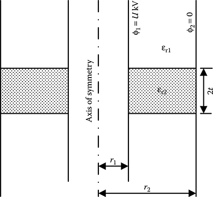
FIGURE 19.3
Schematic representation of the disc insulator considered for optimization study. (Data from Grönewald, H., IEEE Proc. C, 130, 4, 201–205, 1983.)
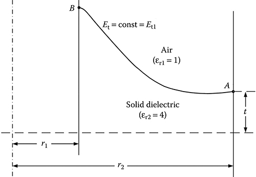
FIGURE 19.4
Optimized contour for a constant tangential field intensity along insulator surface.
19.3.2 Electrode and Insulator Contour Correction with Approximation of Corrected Contour
Stih [11] proposed a procedure for optimization of electrode and insulation system combining the approach of varying the distances between contour points and then approximating the corrected contour by circular arcs. The procedure was applied for optimizing axi-symmetric configurations. In the proposed approach, the target was to attain uniform distribution of normal field intensity on the electrode surface and uniform distribution of tangential field intensity on the insulator surface. The contour correction principle, as presented in Reference [11] is described below.

FIGURE 19.5
Tangential field intensity distribution along the starting and optimized insulator contours.
As shown in Figure 19.6a if the point 1 moves to 1′ in the normal direction while the potential VA of the electrode is kept constant, then the normal field intensity EA will increase to EA′, such that
where:
EA′ > EA as l1′ 2 < l12

FIGURE 19.6
Principle of contour correction: (a) for electrode and (b) for insulator.
On the other hand, if the point P on the insulator surface moves to the P′, as shown in Figure 19.6b, along the equipotential line, that is, normal to the electric field intensity, then the tangential field intensity decreases from EtP to EtP’ such that
where:
EOP’ < EOP as lOP’ > lOP
The quantum of displacement of contour points was controlled by moving the contour points in proportion to the difference between the actual and desired values of field intensity. Let be the vector that defines the ith contour point on the actual contour, while be the vector that defines the ith contour point on the corrected contour. Then these two vectors were related as
where:
is the unit vector normal to the electrode or to the electric field intensity at the ith contour point on the surface of electrode or insulator, as the case may be
In Equation 19.19,
where:
where:
Edi is the desired value of electric field intensity
EAi is the value of electric field intensity on the actual contour at the ith contour point
N is the number of contour points for which correction is carried out
f1 is a factor that limits the quantum of displacement of the contour points, as Equations 19.17 and 19.18 are valid only for small displacements. Typically the value of f1 was chosen as 0.1
In the next step of the optimization procedure [11], smooth approximation of the corrected contour was done by circular arcs in the following way. For smooth approximation of a particular set of points H = [Pi,(xi, yi)], i = 1,…,N by a circular arc, the conditions that are to be satisfied are as follows: (1) the centre of the circle should be on a given line y = mh x + ch, (2) the circle passes through the given point Pj(xj,yj) and (3) the circle is the best approximation of the given set of points. With reference to Figure 19.7, it may be written that

FIGURE 19.7
Approximation of a set of points by circular arc.
where:
r is the radius
(x0,y0) are the coordinates of the centre of the circular arc
Considering the conditions given by Equations 19.21 and 19.22, for best approximation the minimum is to be found of the function G, which is given below
For this purpose, the minimum of the function F is to be determined, where F is given as follows:
The conditions to be satisfied for minimum F are
From these conditions a system of equations for the unknown variables x0, y0, r, α and β was obtained, which in turn was reduced to a non-linear equation for x0 that was solved numerically.
Further, the smooth approximation of complex electrode and insulator contours by several circular arcs is based on the fact that two circular arcs are joined smoothly at a point J1 or J2 if the centres of the two circles lie on the line passing through the point J1 or J2, as shown in Figure 19.8.

FIGURE 19.8
Smooth joining of circular arcs.
The optimization process was started by choosing an initial contour from not only electrical considerations but also considering mechanical, thermal and other technical constraints. The electric field distribution was computed numerically using integral equation technique. The distances between the contour points were changed using the following rule: if the maximum field intensity is lower than the allowable value then the distances are decreased and vice versa. The stopping criteria of the optimizations steps were
where:
Emax, Emin and Eallow are maximum, minimum and allowable values of electric field intensities, respectively
fu is the field uniformity factor
fe is the chosen limit of maximum field intensity with respect to allowable field intensity. Typical range of values of fu and fe were 1 < fu < 1.1 and 0.9 < fe < 1, respectively
Stih [11] applied the methodology for optimization of the shielding electrode of a transformer winding. The initial geometry of the system is shown in Figure 19.9, where the shielding electrode is chosen as semicircle. The optimized final geometry of the shielding electrode is shown in Figure 19.10, which was obtained for fu = 1.06 and fe = 0.99 [11].
19.3.3 Parametric Optimization of Insulator Profile
Abdel-Salam and Stanek [12] described a method to obtain uniform tangential field intensity along high-voltage insulator surface by modifying the profile.
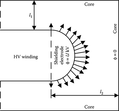
FIGURE 19.9
Initial geometry of shielding electrode with field distribution.

FIGURE 19.10
Final optimized geometry of shielding electrode with field distribution.
In this algorithm actual value of tangential field intensity was used to correct the mathematical expression of the insulator contour to achieve the final optimized profile. In order to search for a profile for which tangential field intensity is uniform along the profile, the following procedure was adopted:
Tangential field intensity values were computed along the non-optimized profile numerically. If the tangential field intensity increases while moving along the axis of the insulator, then the profile radius needs to be increased in that direction.
In order to get a smooth change in the profile radius, pre-defined mathematical expression for the profile was used in this work. While formulating the profile expression, care was taken, so that the contact angle at the insulator–electrode junction remained 90°. In other words, the profile expression must satisfy the right angle contact criterion for the insulator with electrodes. This is necessary to avoid excessive field concentration at the contact points.
As shown in Figure 19.11, the profile radius was proposed to have an exponential variation as given below.
where:
x% of the height h was kept vertical to maintain the right angle contact criterion at both the live and ground electrode ends

FIGURE 19.11
Profile optimization by exponential variation of profile radius.
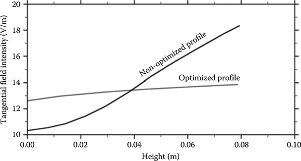
FIGURE 19.12
Distribution of tangential field intensity along non-optimized as well as optimized profiles.
Typically x was chosen to be 5%. DR was the largest value of enlargement in profile radius through exponential increase along the z-direction from the ground end to live end. As a result, the radius of the insulator at the ground end was R0 and that at the live end was R0 + DR.
N number of contour points were chosen along the insulator profile and the tangential field intensities were computed at these points by numerical field computation. Then the value of DR was changed iteratively to the final value DRF to achieve an acceptable degree of uniformity in tangential field intensity along the optimized insulator profile, which is depicted in Figure 19.11. Figure 19.12 shows the tangential field distribution for non-optimized as well as for the optimized profiles [12].
19.4 ANN-Based Optimization of Electrode and Insulator Contours
ANNs offer a completely different approach to problem solving. An ANN is a behavioural model built through learning from a number of examples of the behaviour. It transforms the given data pertaining to a problem into a model or predictor, and then applies this model to the present data to obtain an estimate. ANN has two fundamental features: (1) the ability to represent any function, linear or not, simple or complicated. ANNs are what mathematicians call universal approximators and (2) the ability to learn from representative examples so that model building is automatic. The advantages of ANNs are (1) one goes directly from factual data to the model without any manual work, without tainting the result with oversimplification or pre-conceived ideas and (2) there is no need to postulate a model or to amend it.
Neural networks, with their remarkable ability to derive relationship from complicated or imprecise data, can be used to estimate functions that are too complex to be noticed by either humans or other computerized techniques. A trained neural network can then be used to provide projections in new situations of interest and answer what if questions. For example, if an ANN is trained with the geometric dimensions as input and the electric field intensities at different points as output patterns, then the trained ANN can estimate the electric field intensity for any given dimension without going into complicated process of field computation.
19.4.1 ANN-Based Optimization of Electrode Contour
Chakravorti and Mukherjee [34] applied the inverse logic in optimizing the electrode shape to obtain a uniform normal field intensity along the end profile of a parallel disc electrode arrangement. In this approach, the ANN was trained with the electric field intensities as input patterns and the geometric dimensions as the output patterns. Then the trained ANN was used to predict the geometric dimensions of the electrode to get a uniform field intensity along the electrode end profile. Chakravorti and Mukherjee [34] optimized the end profile of an axi-symmetric electrode arrangement in the form of parallel discs using the above-mentioned inverse logic. For the purpose of training the ANN, input–output patterns need to be generated. These training patterns were generated by numerical field computations carried out for pre-defined electrode shapes for which the end profile was taken to be circular, as shown in Figure 19.13.
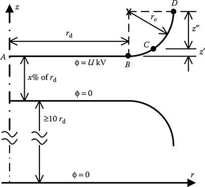
FIGURE 19.13
Parallel disc electrode configuration with circular end profile.
For the purpose of generating the training data, radius of parallel discs and the separation distance between the discs were kept constant at rd and 30% of rd, respectively. NC numbers of different contours were obtained by varying the radius of end profile (re) in steps. For each of these NC contours, electric field intensities were calculated at (NP + 2) number of points on the electrode surface, out of which two were on the parallel surface and the rest NP were on the end profile. The electric field intensities at the (NP + 2) points in each contour were then given as input pattern vector to the ANN, while the coordinates of the NP points on the end profile were given as output pattern vector. The NP points on the end profile were taken at fixed z-coordinates for all the circular end profiles having pre-defined radii. Hence, only the r-coordinates of the NP points were given as output pattern vector. The ANN is thus made up of (NP + 2) and NP neurons in the input and output layers, respectively, and there were NC number of input–output patterns. For preparing the training set, electric field computations were carried out considering the potential of the live electrode as 0.1 kV, where 100 V represented the percent potential difference between the two electrodes.
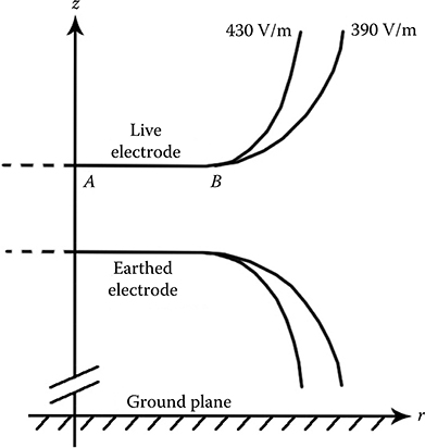
FIGURE 19.14
Optimized end profiles for two values of desired uniform field intensities in the critical domain.
For electrode contour optimization, for every set of input pattern the output pattern was known. Hence, for this problem, ANN with supervised learning was implemented involving multilayer feed-forward network with error-back propagation [34]. After completion of the training process, an optimized end profile was determined as a test case with the desired field intensity value of 390 V/m in the critical domain between B and C on the end profile, as shown in Figure 19.13. For this optimized end profile, as shown in Figure 19.14, electric field computations were carried out to determine the electric field intensities along the end profile to find out the deviation of the test results from the desired value of 390 V/m. MAE in field results along profiles obtained from ANN as output with respect to the desired values was found to be ≈3% [34]. The variation of actual electric field intensity distribution for a desired uniform field intensity of 390 V/m is shown in Figure 19.15 [34].

FIGURE 19.15
Actual field intensity distribution vis-à-vis the desired uniform field intensity in the critical domain of the end profile.
19.4.2 ANN-Based Optimization of Insulator Contour
Using an approach similar to that discussed in Section 19.4.1, Bhattacharya et al. [38] reported ANN-based contour optimization of axi-symmetric insulators in multi-dielectric arrangements to obtain not only uniform but also complex electric field intensity distributions along the insulator surface. For the purpose of generating the training data, electric field computations were carried for conical support insulators having linear contour, as shown in Figure 19.16.
In electric field computations h, h1 and h2 were kept constant. Typically h1 and h2 were taken as 10% of h. NR numbers of different values of R2 were taken when R1 was kept constant. Similarly, NR numbers of different values of R1 were taken when R2 was kept constant. Therefore, there were 2NR numbers of contours for generating the training data. Tangential stresses were calculated at NP numbers of points on all the 2NR numbers of pre-defined insulator surfaces. For each of the NP points, the z-coordinate was kept fixed on all the pre-defined contours. For every one of these 2NR contours, NP tangential field intensities were given to the ANN as input pattern vector and the corresponding r-coordinates of the NP points were given as output pattern vector during training. Therefore, the ANN had NP neurons each for input and output layers and 2NR numbers of input–output training patterns. Multi-layer feed-forward network with error-back propagation as well as resilient propagation were employed for supervised learning of ANN.

FIGURE 19.16
Conical support insulator having linear contour.

FIGURE 19.17
Desired and actual distributions of tangential field intensity along the optimized insulator contour.
After completion of successful training, a normalized uniform tangential field intensity of 0.1 V/cm was desired along the insulator surface, as shown in Figure 19.17. NP values of uniform tangential field intensities at the NP specified points were fed to the trained ANN as inputs and the corresponding r-coordinates of the NP points were obtained as outputs from the trained ANN. These r-coordinates, as obtained from the trained ANN as outputs, along with their respective z-coordinates were then plotted to get the optimized insulator profile, which is shown in Figure 19.18 [38]. Subsequently, with the help of numerical field computation the actual values of tangential field intensities at these NP points on the optimized insulator contour were determined. MAE between the actual and desired tangential field intensities was found to be ≈2% [38]. The actual and desired tangential field intensity distributions along the optimized insulator profile of Figure 19.18 are shown in Figure 19.17.

FIGURE 19.18
Optimized insulator contour as obtained from the trained ANN.
19.5 ANN-Aided Optimization of 3D Electrode–Insulator Assembly
A simplified flow chart, as shown in Figure 19.19, explains the iterative structure of conventional procedure for the optimization of electrode or insulator contours. It is a two-step procedure, in which, electric field distributions are computed by any particular method and design parameters are changed using any optimization algorithm. This two-step procedure strictly separates electric field computation and design parameter modifications. The modification of the design parameters does not require absolute electric field values, but only the error between the actual and desired electric field values in each iterative step. That is why the parameter updation algorithm could be completely separated from electric field computation.
The function estimation ability of ANN was used by Lahiri and Chakravorti [42,43] to modify the flowchart of optimization process shown in Figure 19.19. It has been mentioned in Section 19.4 that if an ANN is trained with the geometric dimensions as input and the electric field intensities as output patterns, then the trained ANN can estimate the electric field intensity for any set of given dimensions without going into detailed electric field computation. Because of decoupling of electric field computation and parameter updation routines in the optimization process, it was possible to replace the electric field computation routine by a trained ANN to get an estimate of the electric field distribution for the values of design parameters in each iterative step. The modified flowchart is shown in Figure 19.20.

FIGURE 19.19
Flowchart of conventional optimization process.
Major saving in computation time was achieved in References [42,43] by coupling a trained ANN in the optimization loop. At each move of the optimization loop, the evaluation of the cost function through electric field computation routine would require, say, T units of time. Now supposing the optimization algorithm requires N number of moves to converge to the optimum value of the cost function, the total time required for the entire optimization process would be N*(T + t) units of time, where t is the execution time of each step of the optimization algorithm. Typically, for any numerical field computation method, the value of T will be of the order of several minutes for real-life 3D configurations. But if the cost function is estimated by a trained ANN, then it requires only a fraction of a second to do so, instead of T minutes. However, in this proposed method, the time consuming part is the training of ANN plus the time required for electric field computation routine to generate the desired number of training sets, which requires several minutes. But, it is to be noted here that the training set is required to be generated only once and the ANN is required to be trained once, too. Hence, any optimization algorithm coupled to a trained ANN offers considerable saving in time for 3D electric field optimization. Another major advantage of the proposed method was that the upper and lower bounds of the design parameters could be easily modified by varying the range of training data for the ANN.

FIGURE 19.20
Flowchart of ANN-aided optimization process.
Lahiri and Chakravorti [42] optimized the 3D electrode–support insulator assembly shown in Figure 19.21 using the above-mentioned methodology employing GA. This configuration is often used in gas-insulated transmission lines (GIL). In this arrangement, the most critical parts of the profiles were (1) the shape of the hole in the electrode through which the support insulator was to be inserted as shown in Figure 19.21b, and (2) the curved profile of the insulator in the middle, as shown in Figure 19.21c. As a result the design parameters chosen for optimization were related to the shape of these critical parts.
In another work, Lahiri and Chakravorti [43] optimized 3D electrode-disc insulator assembly used in GIL shown in Figure 19.22 employing SA for optimization. In this arrangement, the most critical parts of the profiles were the curvatures of the live electrode as well as the disc-type insulator as shown in Figure 19.22b. Consequently, the design parameters chosen for optimization were related to these critical curvatures.
For both these optimization problems, sensitivity studies were carried out first to determine which design parameters of the electrode–insulator assembly are to be modified to get a minimum value of field intensity within the GIL. The most sensitive design parameters were initialized and then modified using the flowchart given in Figure 19.20. The cost function for optimization was maximum value of the electric field intensity, which was minimized through optimization routines such as GA or SA.

FIGURE 19.21
(See colour insert.) 3D electrode–support insulator assembly for optimization: (a) electrode–insulator assembly; (b) live electrode and (c) support insulator.

FIGURE 19.22
(See colour insert.) 3D electrode–disc insulator assembly for optimization: (a) disc-type insulator with live and ground electrodes and (b) live electrode with sectional view of disc insulator.
Objective Type Questions
1. Optimal contours in an insulating system are those that provide
a. A uniform field distribution
b. A desired field distribution
c. Both (a) and (b)
d. None of the above
2. The criterion commonly used for the optimization of electrode contour is the minimization of
a. Radius of curvature
b. Normal component of electric field intensity
c. Tangential component of electric field intensity
d. Both (a) and (b)
3. Optimized profiles of electrodes and insulators are such that
a. Dimensions are minimized for a given voltage rating
b. Usage of space is maximized within the given constraint
c. Cost of installation is minimized
d. All the above
4. If the insulator contour is moved in the direction of the vector normal to the surface, then
a. Tangential field intensity decreases
b. Tangential field intensity increases
c. Normal field intensity decreases
d. Normal field intensity increases
5. Target for insulator contour optimization is achieving
a. Uniform tangential field intensity on the insulator surface
b. Uniform resultant field intensity on the insulator surface
c. Uniform electrostatic pressure on the insulator surface
d. Both (a) and (b)
6. In the case of contour correction technique, insulator contour optimization is done by keeping
a. Potential difference between two successive contour points constant
b. Field intensity difference between two successive contour points constant
c. Distance between two successive contour points constant
d. Both (a) and (c)
7. In the case of contour correction technique, the quantum of displacement of contour points is controlled by moving the contour points in proportion to the difference between the actual and desired values of
a. Electric potential
b. Electric field intensity
c. Electric flux density
d. Both (a) and (b)
8. In the field optimization algorithms, the modification of the design parameters requires
a. Absolute values of electric potential
b. Absolute values of electric field intensity
c. Error between the actual and desired values of electric potential
d. Error between the actual and desired values of the electric field intensity
9. In ANN-aided electric field optimization, it is possible to replace the electric field computation routine by a trained ANN to get an estimate of the electric field distribution because of
a. Decoupling of electric field computation and parameter updation routines
b. Coupling of electric field computation and parameter updation routines
c. Decoupling parameter initialization and parameter updation routines
d. Both (b) and (c)
10. In ANN-aided electric field optimization, the upper and lower bounds of the design parameters could be easily modified by varying the range of
a. Training data of the ANN
b. Testing data of the ANN
c. Both (a) and (b)
d. None of the above
Answers:
1) c;
2) b;
3) d;
4) a;
5) d;
6) d;
7) b;
8) d;
9) a;
10) a
References
1. J. Spielrein, ‘Geometrisches zur elektrischen Festigkeitsrechnung’, Archiv für Elektrotechnik, Vol. 4, pp. 78–85, 1915.
2. W. Rogowski, ‘Die elektrische Festigkeit am Rande des Platten-Kondensators’, Archiv für Elektrotechnik, Vol. 12, pp. 1–14, 1923.
3. N. Félici, ‘Les surfaces á champ électrique constant’, Revue Générale de l’électricité, Vol. 59, pp. 479–501, 1950.
4. H. Singer and P. Grafoner, ‘Optimization of electrode and insulator contours’, Proceedings of the 2nd ISH, Zurich, Switzerland, pp. 111–116, September 9–13, 1975.
5. H. Singer, ‘Computation of optimized electrode geometries’, Proceedings of the 3rd ISH, Milan, Italy, Paper No. 11.06, August 28–31, IEEE North Italy Section Publication, 1979.
6. D. Metz, ‘Optimization of high voltage fields’, Proceedings of the 3rd ISH, Milan, Italy, Vol. 1, Paper No. 11.12, August 28–31, IEEE North Italy Section Publication, 1979.
7. H. Okubo, T. Amemiya and M. Honda, ‘Borda’s profile and electric field optimization by using charge simulation method’, Proceedings of the 3rd ISH, Milan, Italy, August 28–31, IEEE North Italy Section Publication, Paper No. 11.16, 1979.
8. T. Misaki, H. Tsuboi, K. Itaka and T. Hara, ‘Computation of three-dimensional electric field problems and its application to optimum insulator design’, IEEE Transactions on Power Apparatus and Systems, Vol. PAS-101, pp. 627–634, 1982.
9. T. Misaki, H. Tsuboi, K. Itaka and T. Hara, ‘Optimization of three-dimensional electrode contour based on surface charge method and its application to insulation design’, IEEE Power Engineering Review, Vol. 82, p. 44, 1983.
10. H. Grönewald, ‘Field optimisation of high-voltage electrodes’, IEEE Proceedings C – Generation, Transmission and Distribution, Vol. 130, No. 4, pp. 201–205, 1983.
11. Z. Stih, ‘High voltage insulating system design by application of electrode and insulator contour optimization’, IEEE Transactions on Electrical Insulation, Vol. 21, No. 4, pp. 579–584, 1986.
12. M. Abdel-Salam and E.K. Stanek, ‘Field optimization of high-voltage insulators’, IEEE Transactions on Industry Applications, Vol. 22, No. 4, pp. 594–601, 1986.
13. M. Abdel-Salam and E.K. Stanek, ‘Optimizing field stress on HV insulators’, IEEE Transactions on Electrical Insulation, Vol. 22, No. 1, pp. 47–56, 1987.
14. W. Mosch, M. Dietrich, E. Lemke and W. Hauschild, ‘Statistical design of large UHV electrodes in air’, IEEE Proceedings A – Physical Science, Measurement and Instrumentation, Management and Education – Reviews, Vol. 133, No. 8, pp. 547–551, 1986.
15. K. Kato, X. Han and H. Okubo, ‘Optimization technique of high voltage electrode contour considering V-t characteristics based on volume-time theory’, Proceedings of the 11th ISH, London, Vol. 2, pp. 123–126, August 23–27, IEE (UK) Publication, 1999.
16. J. Liu and J. Sheng, ‘The optimization of the high voltage axi-symmetrical electrode contour’, IEEE Transactions on Magnetics, Vol. 24, No. 1, pp. 39–42, 1988.
17. J. Liu, E.M. Freeman, X. Yang and J. Sheng, ‘Optimization of electrode shape using the boundary element method’, IEEE Transactions on Magnetics, Vol. 26, No. 5, pp. 2184–2186, 1990.
18. T.N. Judge and J. Lopez-Roldan, ‘Optimization of high voltage equipment design using boundary element method based electromagnetic analysis tools’, Proceedings of the 11th ISH, London, Vol. 2, pp. 140–143, August 23–27, IEE (UK) Publication, 1999.
19. J.D. Welly, ‘Optimization of electrode contours in high voltage equipment using circular contour elements’, Proceedings of the 5th ISH, Braunschweig, Germany, Paper No. 31.03, August 24–28, 1987.
20. D. Huimin et al., ‘Optimization of high voltage fields of multi-electrode systems’, Proceedings of the 6th ISH, New Orleans, LA, Paper No. 40.03, August 28–September 1, 1989.
21. H.H. Däumling and H. Singer, ‘Investigations on field optimization of insulator geometries’, IEEE Transactions on Power Delivery, Vol. 4, No. 1, pp. 787–793, 1989.
22. W.M. Caminhas, R.R. Saldanha and G.R. Mateus, ‘Optimization methods used for determining the geometry of shielding electrodes’, IEEE Transactions on Magnetics, Vol. 26, No. 2, pp. 642–645, 1990.
23. Z. Fang, J. Jicun and Z. Ziyu, ‘Optimal design of HV transformer bushing’, 3rd International Conference on Properties and Applications of Dielectric Materials, Tokyo, Japan, pp. 434–437, July 8–12, IEEE Publication, 1991.
24. M. Abdel-Salam and A. Mufti, ‘Optimizing field stress on high voltage bushings’, IEEE International Symposium on Electrical Insulation, Pittsburg, PA, pp. 225–228, June 5–8, IEEE Publication, 1994.
25. E.S. Kim et al., ‘Electric field optimization using NURB curve and surface’, Transactions of IEEJ, Vol. 113-B, No. 10, pp. 1081–1087, 1993.
26. K. Kato et al., ‘A highly efficient method for determination of electric field optimum contour on high voltage electrode’, Proceedings of the 9th ISH, Graz, Austria, Paper No. 8358, August 28–September 1, 1995.
27. J.A.G. Gacia et al., ‘Contour optimization of high-voltage insulators by means of smoothing cubic splines’, Proceedings of the 9th ISH, Graz, Austria, Paper No. 8343, August 28–September 1, 1995.
28. H. Okubo et al., ‘The development of electric field optimization technique using personal computer’, Proceedings of the 8th ISH, Yokohama, Japan, Paper No. 11.04, August 23–27, 1993.
29. K. Kato, M. Hikita, N. Hayakawa, Y. Kito and H. Okubo, ‘Development of personal-computer-based high efficient technique for electric field optimization’, European Transactions on Electrical Power Engineering, Vol. 5, pp. 401–407, 1995.
30. C. Trinitis et al., ‘Accelerated 3-D optimization of high voltage apparatus’, Proceedings of the 9th ISH, Graz, Austria, Paper No. 8867, August 28–September 1, 1995.
31. C. Trinitis, ‘Field optimization of three dimensional high voltage equipment’, Proceedings of the 11th ISH, London, Vol. 2, pp. 75–78, August 23–27, IEE (UK) Publication, 1999.
32. J.A. Gomollon, G. Gonzalez-Filgueira and E. Santome, ‘Optimization of high voltage insulators within three dimensional field distributions’, Proceedings of the 6th IEEE ICPADM, Xian, China, Vol. 2, pp. 629–632, June 21–26, IEEE Publication, 2000.
33. J.G. Leopold, U. Dai, Y. Finkelstein and E. Weissman, ‘Optimizing the performance of flat-surface, high-gradient vacuum insulators’, IEEE Transactions on Dielectrics & Electrical Insulation, Vol. 12, No. 3, pp. 530–536, 2005.
34. S. Chakravorti and P.K. Mukherjee, ‘Application of artificial neural networks for optimization of electrode contour’, IEEE Transactions on Dielectrics & Electrical Insulation, Vol. 1, No. 2, pp. 254–264, 1994.
35. K. Bhattacharya, S. Chakravorti and P.K. Mukherjee, ‘An application of artificial neural network in the design of toroidal electrodes’, Journal of the IE(I), Pt. CP, Vol. 76, pp. 14–20, 1995.
36. P.K. Mukherjee, C. Trinitis and H. Steinbigler, ‘Optimization of HV electrode systems by neural networks using a new learning method’, IEEE Transactions on Dielectrics & Electrical Insulation, Vol. 3, No. 6, pp. 737–742, 1996.
37. H. Okubo, T. Otsuka, K. Kato, N. Hayakawa and M. Hikita, ‘Electric field optimization of high voltage electrode based on neural network’, IEEE Transactions on Power Systems, Vol. 12, No. 4, pp. 1413–1418, 1997.
38. K. Bhattacharya, S. Chakravorti and P.K. Mukherjee, ‘Insulator contour optimization by artificial neural network’, IEEE Transactions on Dielectrics & Electrical Insulation, Vol. 8, No. 2, pp. 157–161, 2001.
39. A. Chatterjee, A. Rakshit and P.K. Mukherjee, ‘A self-organizing fuzzy inference system for electric field optimization of HV electrode systems’, IEEE Transactions on Dielectrics & Electrical Insulation, Vol. 8, No. 6, pp. 995–1002, 2001.
40. P.G. Alotto, B. Brandstätter, E. Cela, G. Fürntratt, C. Magele, G. Molinari, M. Nervi, K. Preis, M. Repetto and H.R. Richter, ‘Stochastic algorithms in electromagnetic optimization’, IEEE Transactions on Magnetics, Vol. 34, No. 5, pp. 3674–3684, 1998.
41. Z. Guoqiang, Z. Yuanlu and C. Xiang, ‘Optimal design of high voltage bushing electrode in transformer with evolution strategy’, IEEE Transactions on Magnetics, Vol. 15, pp. 1690–1693, 1999.
42. A. Lahiri and S. Chakravorti, ‘Electrode-spacer contour optimization by ANN aided genetic algorithm’, IEEE Transactions on Dielectrics & Electrical Insulation, Vol. 11, No. 6, pp. 964–975, 2004.
43. A. Lahiri and S. Chakravorti, ‘A novel approach based on simulated annealing coupled to artificial neural network for 3D electric field optimization’, IEEE Transactions on Power Delivery, Vol. 20, No. 3, pp. 2144–2152, 2005.
44. S. Banerjee, A. Lahiri and K. Bhattacharya, ‘Optimization of support insulators used in HV systems using support vector machine’, IEEE Transactions on Dielectrics & Electrical Insulation, Vol. 14, No. 2, pp. 360–367, 2007.
45. P. Kitak, J. Pihler, I. Ticar, A. Stermecki, C. Magele, O. Bíró and K. Preis, ‘Use of an optimization algorithm in designing medium-voltage switchgear insulation elements’, IEEE Transactions on Magnetics, Vol. 42, No. 4, pp. 1347–1350, 2006.
46. K. Kato, S. Kaneko, S. Okabe and H. Okubo, ‘Optimization technique for electrical insulation design of vacuum interrupters’, IEEE Transactions on Dielectrics & Electrical Insulation, Vol. 15, No. 5, pp. 1456–1463, 2008.
47. X. Liu, Y. Cao, F. Wen and E. Wang, ‘Optimization of extra-high-voltage SF6 circuit breaker based on improved genetic algorithm’, IEEE Transactions on Magnetics, Vol. 44, No. 6, pp. 1138–1141, 2008.
48. H.J. Ju, K.C. Ko and S.K. Choi, ‘Optimal design of a permittivity graded spacer configuration in a gas insulated switchgear’, Journal of Korean Physical Society, Vol. 55, No. 5, p. 1803, 2009.
49. H. Ju, B. Kim and K. Ko, ‘Optimal design of an elliptically graded permittivity spacer configuration in gas insulated switchgear’, IEEE Transactions on Dielectrics & Electrical Insulation, Vol. 18, No. 4, pp. 1268–1273, 2011.
50. S. Monga, R.S. Gorur, P. Hansen and W. Massey, ‘Design optimization of high voltage bushing using electric field computations’, IEEE Transactions on Dielectrics & Electrical Insulation, Vol. 13, No. 6, pp. 1217–1224, 2006.
51. M.R. Hesamzadeh, N. Hosseinzadeh and P. Wolfs, ‘An advanced optimal approach for high voltage AC bushing design’, IEEE Transactions on Dielectrics & Electrical Insulation, Vol. 15, No. 2, pp. 461–466, 2008.
52. C. Trinitis, ‘Automatic high voltage apparatus optimization: Making it more engineer-friendly’, International Symposium on Parallel Computing in Electrical Engineering, Bialystok, Poland, September 13–17, IEEE Publication, 2006.