
18
Numerical Computation of Electric Field in High-Voltage System – Case Studies
ABSTRACT Several components, which are widely used in high-voltage systems, are critical in nature from the viewpoint of failure due to electrical discharges. Two common examples of such components are bushings and cable terminations. Insulators that are used in large numbers in all highvoltage systems are prone to failure due to surface pollution or surface wetting. These unwanted failures could be prevented by appropriate design only if the electric field distribution is estimated accurately through numerical field computations. However, results of numerical field computations need to be validated using benchmark models for which analytical solutions are available. This chapter presents a few such benchmark models and reports results of electric field analysis in bushings, cable terminations as well as insulators under various operating conditions.
18.1 Introduction
Numerical computation of electric field for high-voltage system components and devices are carried out to determine the adequacy of insulation to reliably withstand electric stresses that may arise in the system. Some of these components are critical to the system. For example, if the bushing of a transformer fails, then it leads to terminal short circuit and causes very high fault levels. Again bushings are of different types depending on the system voltage level. Thus, field distribution within bushings is to be determined accurately, so that proper insulation could be provided to prevent any unwanted failure. Similarly, cable terminations, where the cable is connected to another equipment, are critical components that are prone to failure due to excessive field concentration. Stress diverters of suitable design are used in such cable terminations, the shapes of which are normally finalized through extensive electric field computations. Insulators that are able to withstand electric stresses satisfactorily under dry condition may not be able to withstand electric stresses under wet or polluted conditions due to change in the field distribution. In order to ensure safe operation of insulators under all environmental conditions, it is necessary to find electric field distribution in and around insulators in all such conditions. However, there is a need for validating the results obtained from numerical field analysis. This is typically done by considering benchmark models for which analytical solutions are available. Taking the analytical results as reference, the accuracy of numerical results is determined through comparison of analytical and numerical results.
18.2 Benchmark Models for Validation
Two benchmark models are commonly used for validation of numerical codes for purely capacitive field analysis as detailed below: (1) for two-dimensional system – cylinder in uniform external field and (2) for axi-symmetric system – sphere in uniform external field. For capacitive-resistive field in axi-symmetric system, a dielectric sphere in uniform external field is used as a benchmark model.
18.2.1 Cylinder in Uniform External Field
Analytical solutions for capacitive field distribution in the case of a cylinder in uniform external field have been discussed in detail in Section 10.3. For validation of numerical output, results for a conducting cylinder as well as a dielectric cylinder in uniform external field are used. In the case of a conducting cylinder in uniform field, numerical results for electric potential could be compared to that obtained from Equation 10.54, while numerically computed values of electric field intensity components could be compared to the corresponding values obtained from Equations 10.55 and 10.56. For a dielectric cylinder in uniform external field, Equations 10.65 and 10.66 are used for validating results for electric potential and the results for electric field intensity components are validated using the partial derivatives of Equations 10.65 and 10.66.
18.2.2 Sphere in Uniform External Field
Electric field in and around a sphere in uniform external field has been solved analytically in Section 10.2 in the absence of resistivity of dielectric material, that is, in the case of purely capacitive field. These analytical solutions are useful for validating numerical field computation results in axi-symmetric systems. For a conducting sphere in uniform external field, Equations 10.22 through 10.24 are used for validating results for electric potential and electric field intensity components, respectively. For a dielectric sphere in uniform external field, Equations 10.33 and 10.34 are used for validating results for electric potential within and outside the dielectric sphere, respectively. Results for electric field intensity components within and outside the dielectric sphere could be validated using the partial derivatives of Equations 10.33 and 10.34, respectively.
18.2.3 Dielectric Sphere Coated with a Thin Conducting Layer in Uniform External Field
Results for capacitive-resistive field in axi-symmetric system could be validated using the benchmark model comprising a dielectric sphere coated with a thin conducting layer in uniform sinusoidal external field [1]. The configuration is schematically shown in Figure 18.1. Uniform sinusoidal field is represented as eu = Eum sin ωt. In this configuration, for the dielectric sphere as well as the surrounding dielectric medium conductivity is zero, that is, σ1 = σ3 = 0. For the thin conducting layer on the dielectric sphere, relative permittivity is unity and conductivity (σ2) is variable. Radius of the dielectric sphere is r and the thickness of conducting layer is t.
Analytical solution for maximum electric field intensity at the point P, as shown in Figure 18.1, is given by
where:

FIGURE 18.1
Dielectric sphere coated with a thin conducting layer in uniform sinusoidal external field.
18.3 Electric Field Distribution in the Cable Termination
Terminations are required in the case of connecting the cable to another line or a busbar or to equipments such as a transformer or a switchgear. A high-voltage cable termination typically provides (1) adequate electric stress control for the cable insulation shield terminus; (2) comprehensive external leakage insulation between the high-voltage conductor(s) and grounded ends and (3) proper sealing to prevent the entry of the external environmental elements, for example, moisture and corrosive chemicals, into the cable and also to maintain the pressure, if any, within the cable system. The requirements of an AC cable termination are detailed in IEEE Std 48-1975.
In a co-axial shielded cable, the electric field does not vary along the cable axis and there is variation in electric field only in the radial direction. In terminating a shielded cable, it is necessary to remove the cable insulation shield up to a certain distance from the exposed conductor, depending on the voltage level of the cable and properties of dielectric media in use. The removal of the insulation shield results in a discontinuity in the axial geometry of the cable. As a result the electric field is no longer invariant along the cable axis, but exhibits variations along all three Cartesian axes, which can be suitably modelled by axi-symmetric representation.
Electric flux lines emanating from the conductor converge in the vicinity of the shield discontinuity at the end of the shield causing high electric stresses in this area. Such high stresses may cause premature failure of the cable. But more importantly partial discharges will occur continuously at the site of highfield concentration, which will shorten the life of the cable significantly. Hence, cable terminations must provide stress control to reduce the stresses occurring near the end of the shield. Two commonly used methods for stress control in cable terminations are (1) geometric stress control, in which a stress cone is used, which optimizes the geometry at the terminating discontinuity in order to reduce the stresses at that location. The stress cones use the geometrical solution by controlling the capacitance in the area of the insulation shield terminus and (2) capacitive stress control, in which a material of high dielectric permittivity of the order of 30 is applied on the cable dielectric at the termination. Located near the end of the shield discontinuity, the material changes the electric field distribution in a controlled manner along the entire area where the shielding has been removed.
The problem of the cable-termination design would have been simple had there been no constraint on spacing between the conductors. But for many installations, space requirements put a limit on the practical distance that can be maintained between conductors. Consequently, the determination of electric field distribution in and around the cable termination is of practical importance. This section presents the results of electric field analysis of a typical cable termination used in 220 kV system.
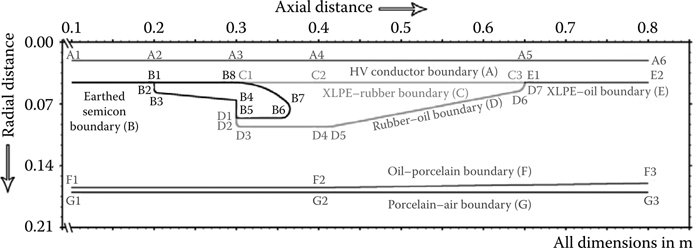
FIGURE 18.2
(See colour insert.) Geometry and boundaries of cable termination under study.
The cable termination for a single-core cable with a porcelain outer cover, as shown in Figure 18.2, is modelled as an axi-symmetric system, where the radial distances are taken from the axis of symmetry. Relative dielectric permittivities that are considered in modelling the cable termination are as follows: (1) cross-linked polyethylene (XLPE) – 2.3, (2) insulation grade rubber – 2.8, (3) oil – 2.2 and (4) porcelain – 6.0.
The various boundaries that are considered in this study are shown in Figure 18.2. Following are the abbreviations that are used in this case: (1) high-voltage (HV) conductor surface – boundary A, (2) earthed semi-conducting surface – boundary B, (3) XLPE–rubber interface – boundary C, (4) rubber–oil interface – boundary D, (5) XLPE–oil interface – boundary E, (6) oil–porcelain interface – boundary F and (7) porcelain–air interface – boundary G. For simplicity, the outer surface of the porcelain cover is taken as cylindrical.
Figure 18.3 shows the plot of normal, tangential and the resultant stresses along the HV conductor boundary. Electric stresses are plotted from A1 to A6 with reference to Figure 18.2. As it is a conductor boundary, the tangential stresses are negligible and hence the normal and resultant stresses are same. The maximum stress occurs between A1 to A3 where the semi-conducting surface is co-axial with the XLPE insulation.
Figure 18.4 shows the plot of normal, tangential and the resultant stresses along the earthed semi-conducting surface. Electric stresses are plotted from B1 to B8 with reference to Figure 18.2. Maximum electric stress occurs between B8 to B1 where the semi-conducting boundary is co-axial with the XLPE insulation. Tangential stresses are negligible except at B8 where very acute angle is formed with XLPE–rubber boundary. Theoretically, such tangential stresses should not occur near B8 as it is a conducting boundary. These stresses arise due to error in numerical simulation of boundary involving very acute angle.

FIGURE 18.3
(See colour insert.) Electric stresses along the high-voltage conductor surface.
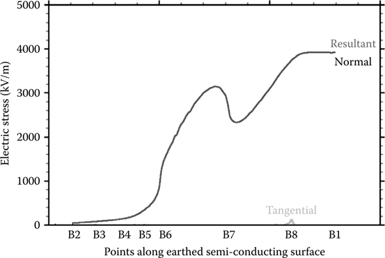
FIGURE 18.4
(See colour insert.) Electric stresses along the semi-conducting surface.
Figure 18.5 depicts the plot of normal, tangential and the resultant stresses on the rubber side along the XLPE–rubber interface. Electric stresses are plotted from C1 to C3 with reference to Figure 18.2. Maximum resultant stresses occur at the zone near C1, where the rubber insulation meets the semiconducting surface making very acute angle. Tangential stresses are significant around location C2.

FIGURE 18.5
Electric stresses on the rubber side along the XLPE-rubber interface.
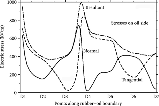
FIGURE 18.6
Electric stresses on the oil side along the rubber–oil interface.
The plot of normal, tangential and resultant stresses along the rubber–oil interface is presented in Figure 18.6. Electric stresses are plotted from D1 to D7 with reference to Figure 18.2. Maximum stresses occur at the zone near D4 where the rubber starts converging towards the XLPE surface.
Figure 18.7 shows the equipotential lines for the cable termination shown in Figure 18.2.

FIGURE 18.7
(See colour insert.) Equipotential lines for the cable termination.
18.4 Electric Field Distribution around a Post-Type Insulator
Post-type insulators usually act as support or spacer of high-voltage electrode with respect to earthed frame or plane. Typically, post-type insulators are surrounded by gaseous dielectric such as air or sulphur hexafluoride (SF6). Knowledge of the electric field distribution around an insulator is necessary to assure reliability in operation of high-voltage system. Chakravorti and Mukherjee [2] reported a detailed study on electric field distribution around a post-type insulator without as well as with surface pollution under power frequency as well as impulse voltages. In this section, results of a similar study have been presented.
The post-type insulator considered for electric field computation is shown in Figure 18.8. The insulator made of porcelain is stressed between two electrodes and is surrounded by air. The electrode–insulator assembly is an axi-symmetric configuration, having two dielectric media, namely, porcelain (εr = 6) and air. Electric field computations have been carried out for uniform surface pollution for which a constant value of surface resistivity is considered along the entire surface of the insulator. For field computation with partial surface pollution different values of surface resistivity have been considered at different locations on the insulator surface. The severity of surface pollution depends on the type of pollution, for example, marine pollution, industrial pollution, and dryness of the pollution. Surface resistivity of pollution layer decreases drastically as the pollution layer is wetted. As a result field computations are carried out over a wide range of surface resistivity from 1015 to 104 Ω in order to simulate varying degrees of surface pollution severity.
18.4.1 Effect of Uniform Surface Pollution
Results of field computations under power frequency (50 Hz) voltage show that the field distribution is capacitive in nature for ρs ≥ 1011 Ω and it is resistive in nature for ρs ≤ 108 Ω. In between the field is capacitive-resistive in nature. Figure 18.9 presents the potential distribution along the insulator surface showing the change in field nature from capacitive to resistive with the change in surface resistivity. Figure 18.10 shows the variation of resultant stress along the insulator surface for capacitive as well as resistive fields.

FIGURE 18.8
Post-type insulator stressed between two electrodes.

FIGURE 18.9
Potential distribution along the insulator surface under power frequency voltage with uniform surface pollution.
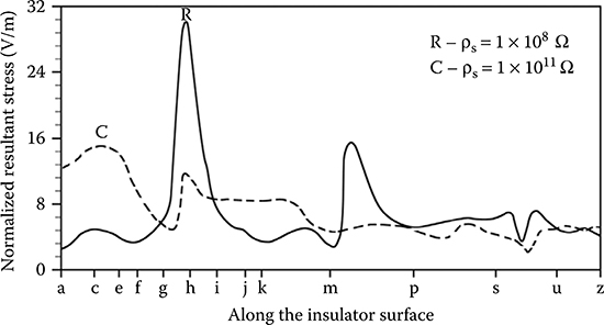
FIGURE 18.10
Resultant stress distribution along the insulator surface under power frequency voltage for capacitive and resistive fields.
The stresses are reported for air side of the porcelain–air interface from the viewpoint of the surface flashover, which occurs in air. It may be seen that the highest resultant stress in the case of resistive field is nearly two times higher than that in the case of capacitive field and occurs near the tip of the topmost shed of the insulator.
Charges that may be present around the insulator surface are drawn on the insulator surface by the normal component of electric stress, whereas the movement of charges on the insulator surface is caused by the tangential component of electric stress. Further charges are generated around the insulator surface due to high resultant stress. Thus, higher resultant stresses in resistive field will generate more charges around the insulator. More charges will then be drawn on the insulator surface by the normal component of electric stress, which under the influence of the tangential component will move along the insulator surface. As a result, the surface leakage current will increase in the case of resistive field compared to capacitive field. It is known that the onset of surface flashover is related to a critical surface leakage current. Hence, higher surface leakage current for resistive field will increase the possibility of surface flashover of the insulator.
18.4.2 Effect of Partial Surface Pollution
Figures 18.11 and 18.12 present the potential and resultant stress distribution, respectively, along the insulator surface for uniform as well as partial surface pollution. In the case of partial surface pollution, the section of the insulator surface from a to h, as shown in Figure 18.8, is considered to be polluted and hence the surface resistivity in this section is taken to be 108 Ω corresponding to resistive field, whereas the rest of the insulator surface is considered to be pollution free for which surface resistivity is taken to be 1011 Ω, corresponding to capacitive field. This case of partial surface pollution is found to be most onerous, as tangential stress is more than twice and the resultant and normal stresses are about 1.6 times higher than the corresponding values for resistive field. These results clearly indicate the danger posed by partial surface pollution.

FIGURE 18.11
Potential distribution along the insulator surface under power frequency voltage with uniform and partial surface pollution vis-a-vis no surface pollution.

FIGURE 18.12
Resultant stress distribution along the insulator surface under power frequency voltage with uniform and partial surface pollution.
18.4.3 Effect of Dry Band
Researchers have recognized that failure of insulators very often is caused by dry bands in the pollution layer on the insulator surface. The dry band can be simulated by a zone of high resistivity in the uniformly polluted surface having a low surface resistivity. The width of the dry band can be varied by varying the length of the zone having high resistivity.
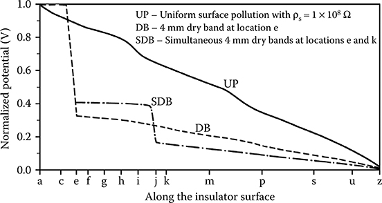
FIGURE 18.13
Potential distribution along the insulator surface under power frequency voltage with dry band and uniform surface pollution.

FIGURE 18.14
Resultant stress distribution along the insulator surface under power frequency voltage with dry band.
Figures 18.13 and 18.14 present the potential and resultant stress distribution, respectively, along the insulator surface for dry band as well as uniform surface pollution. As a thumb rule, many researchers assume that the entire potential difference between the electrodes appears across the dry band. But from the results of field computation it is possible to determine exactly how much potential appears across the dry band and what will be the stresses due to the dry band. These results are very helpful in the studies related to growth of dry band on the insulator surface and it may be stated that the growth of dry band depends on the width as well as the location of the dry band on the insulator surface, as the potential across the dry band depends on these two factors.
Figures 18.13 and 18.14 also show the effect of two simultaneously occurring dry bands on potential and resultant stresses, respectively. It may be seen that if multiple dry bands occur at the same time on the insulator surface, then the resultant stresses are reduced as compared to the occurrence of a single dry band.
18.4.4 Impulse Field Distribution
Electric field computations could be extended to study the field distribution under both lightning and switching impulses. The standard waveshape of lightning impulse voltage is 1.2/50 μs and that for switching impulse is 250/2500 μs. Because the effective frequency of impulse voltage is much higher than power frequency, the value of surface resistivity for which the field will be capacitive or resistive under impulse voltage will be much lower than that for power frequency. Further, the effective frequency of lightning impulse is higher than that for switching impulse and hence the transition of field from capacitive to resistive occurs at lower values of surface resistivity for lightning impulse compared to those for switching impulse.
Results of electric field computations show that for switching impulse the field is capacitive for ρs ≥ 109 Ω and resistive for ρs ≤ 106 Ω, while for lightning impulse the field is capacitive for ρs ≥ 107 Ω and resistive for ρs ≤ 104 Ω.
18.5 Electric Field Distribution in a Condenser Bushing
Bushings are used when a high-voltage conductor is to pass through a barrier having a different potential, for example, an earthed metal tank or an earthed wall. As a result bushings are integral parts of high-voltage equipment such as transformers and shunt reactors. For high-voltage equipment, condenser bushings fitted with cylindrical floating potential electrodes are preferred in practice, as the field nature in a condenser bushing is much less non-linear than the traditional porcelain bushing. The critical region of a bushing from the viewpoint of electrical stress is the zone where the distance between the high-voltage conductor and the barrier is minimum. If the electric field intensity in the critical zone exceeds the breakdown strength of the dielectric used, then discharge will start in this zone. Such discharges may grow and lead to complete breakdown of the bushing. Electric field distribution in and around an outdoor bushing is governed by bushing geometry, permittivity and volume as well as surface resistivities of dielectric media. Out of these factors, surface resisitivity of the outer cover of the bushing plays a major role in determining the field distribution, as it is the most variable parameter affected by atmospheric conditions. Researchers have identified that the deposition of pollution on the outer cover and wetting of pollution layer by fog or condensation are major causes of outdoor bushing failure. Breakdown of bushing is equivalent to terminal short circuit of the equipment such as transformer and results in very high fault levels causing severe damage to the equipment in particular and the system is general. Considering all these practical aspects, Chakravorti and Steinbigler [3] reported detailed results of capacitive-resistive field computation in and around a condenser bushing considering volume and surface resistivities. Results of a similar study are presented in this section.
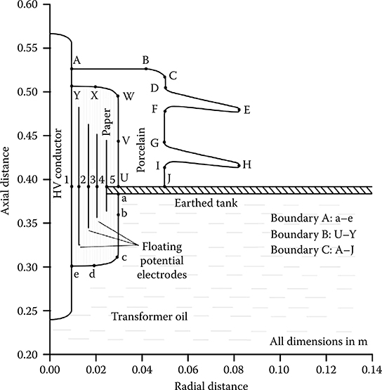
FIGURE 18.15
Condenser bushing arrangement considered for field computation.
Figure 18.15 shows the condenser bushing configuration for which capacitive-resistive field computations have been carried out. It comprises a central conductor that is cylindrical in shape, three cylindrical floating potential electrodes embedded in paper, a porcelain outer cover and an earthed metal tank filled with transformer oil. Thus, the configuration under study is taken to be an axi-symmetric one having four dielectric media, namely, paper (εr = 5), transformer oil (εr = 2.2), porcelain (εr = 6) and air (εr = 1). The potential of the central conductor is considered to be sinusoidal of frequency 50 Hz. For the bushing shown in Figure 18.15 there are three dielectric–dielectric boundaries: (1) paper–oil interface – boundary A, (2) paper–porcelain interface – boundary B and (3) porcelain–air interface – boundary C. Surface resistivity of three boundaries are considered as follows: (1) for boundary A, ρsA is taken to be always uniform; (2) for boundary B, ρsB is taken to be always infinite and (3) for boundary C, ρsC is taken to be both uniform as well as non-uniform to take into account uneven surface pollution. Considering aging-related degradation of paper and oil, volume resistivities of paper (ρvp) and oil (ρvo) have been taken to be high for new condition and low for aged condition, whereas the volume resistivity of porcelain is taken to be always infinite considering very little degradation.
Results of field computations for the following seven cases have been noted to be significant and are presented below: (1) Case 1 – purely capacitive field with infinite surface and volume resistivities; (2) Case 2 – uniform ρsC = 107 Ω and ρsA = ρvp = ρvo = ∞; (3) Case 3 – ρvp = 106 Ω.m and ρsA = ρsC = ρvo = ∞; (4) Case 4 – ρvp = ρvo = 106 Ω.m, uniform ρsA = 106 Ω and ρsC = ∞; (5) Case 5 – ρsC = 107 Ω between A and E while ρsC = ∞ on rest of boundary C, as shown in Figure 18.15, and ρsA = ρvp = ρvo = ∞; (6) Case 6 – as in Case 5 with ρvp = 106 Ω.m and ρsA = ρvo = ∞ and (7) Case 7 – ρvo = 106 Ω.m and ρsA = ρsC = ρvp = ∞.
Figure 18.16 shows the variation of resultant field intensity along the line 1-2-3-4-5 depicted in Figure 18.15, where 2, 3 and 4 correspond to the locations of the three floating potential electrodes from left to right. This zone is the critical region within the bushing. From Figure 18.16 it may be seen that electric stress near HV conductor and earthed tank are highest for Case 6 and Case 3, respectively, and are lowest for Case 3 and Case 6, respectively. Figure 18.16 also shows that partial pollution of boundary C along with a lower volume resistivity of paper insulation (Case 6) causes highest electric stresses in the critical zone.

FIGURE 18.16
Electric stress distribution in the critical zone of the bushing.
Figure 18.17 shows electric stress distribution along the paper–oil boundary (boundary A) for different cases, where the stresses are determined for the oil side of the interface. It may be noted that in all the cases where the volume resistivities of paper and oil have been taken to be low electric stresses are higher. Moreover, when the volume resistivities are taken to be low, then a lower value of ρsA does not affect electric stresses much. For a low value of ρvp (Case 3), the maximum stress occurs at location c on paper–oil boundary, while the maximum stress occurs at location e when volume resistivity of oil (ρvo) is taken to be low (Case 7).

FIGURE 18.17
Electric stress distribution along the paper–oil boundary.

FIGURE 18.18
Electric stress distribution along the paper–porcelain boundary.
Electric stresses on the paper side of the paper–porcelain boundary (boundary B) are shown in Figure 18.18. It shows that for purely capacitive field (Case 1) electric stresses near the point V on boundary B are high, although the highest stress occurs at the point Y. However, for the other cases the stresses at the location Y are relatively lower. From Figure 18.18 it is also clear that partial pollution of boundary C (Case 5) increases the stresses near the location V significantly. Results of computations show that the stresses along boundary B are affected much more by a lower value of ρvp than uniform or non-uniform ρsC.
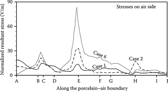
FIGURE 18.19
Electric stress distribution along the porcelain–air boundary.
Electric stresses as computed on the air side of porcelain–air boundary (boundary C) are shown in Figure 18.19. It may be seen that for purely capacitive field (Case 1) electric stresses are comparatively lower. The difference between the maximum and minimum stresses on boundary C is higher for uniform surface pollution (Case 2) than capacitive field. For uniform surface pollution the maximum stress occurs at location E on boundary C. This result is similar to that obtained for uniform surface pollution of porcelain post insulator, as shown in Figure 18.10. Partial surface pollution increases the stresses to a great extent and for Case 6, the maximum stress is quite high at location E. Detailed results of computations revealed that a lower value of ρvp increases the stresses on boundary C to some extent even when the outer surface is uniformly or partially polluted.
18.6 Electric Field Distribution around a Gas-Insulated Substation Spacer
Fully encapsulated and compact SF6 gas-insulated substation (GIS) is considered an integral part of modern-day power installations. Major advantages of GIS are high reliability and compactness achieved by compressed SF6 gas insulation. At the same time, the downsizing of GIS leads to high electric field intensities. Basic insulation components of GIS are SF6 gas and solid spacers. In this respect, it has been recognized that the breakdown strength of GIS is mainly influenced by the solid spacers. Both experimental and numerical studies demonstrate that electric field distribution and insulation behaviour at SF6/spacer interface contribute most towards the failure of spacers. In order to improve the dielectric performance of epoxy spacers by properly shaping the gas–dielectric interfaces, detailed studies on the electric field distribution and optimization along the profile of the gas–dielectric interface in GIS have been reported in the literature [4,5]. In this section, the results of electric field computations for a GIS comprising four components, namely, a central HV conductor, epoxy spacer, SF6 gas and metallic enclosure, are presented. As suggested in the literature, computations have been carried out considering uncoated as well as coated spacer. The coating of the spacer is considered to have a surface resistivity of the order of 107 Ω.

FIGURE 18.20
(See colour insert.) GIS configuration considered for electric field computation.
Figure 18.20 shows the axi-symmetric configuration of the GIS for which electric field computations have been carried out. The dimensions of the GIS are commensurate to voltage rating of 110 kV. Relative permittivity of epoxy spacer has been taken to be 5 and that of SF6 as 1.005. The HV conductor is inserted into the solid spacer from the viewpoint of field reduction at the conductor–spacer–gas triple junction. The condition of solid spacer touching the conductor at right angle has also been maintained. All results are presented in a normalized format.

FIGURE 18.21
Electric field intensity along spacer surface on side 1 for capacitive field.
For uncoated spacer, resultant electric field intensity as well as the two components, namely, normal and tangential, along the spacer surface on side 1 has been presented in Figure 18.21. For this case, surface resistivity of the epoxy spacer is assumed to be infinite, which corresponds to capacitive field distribution. Similar distribution of electric field intensities along the spacer surface on side 2 have been presented in Figure 18.22. Both Figures 18.21 and 18.22 show that the stresses have been reduced near the HV conductor due to metal insert electrode design. On the other hand, such electrode design has shifted the maximum stresses to occur somewhere in the mid region of the spacer surface on both side 1 and side 2.
For coated spacer, resultant, normal and tangential field intensities along the spacer surface on side 1 have been presented in Figure 18.23. For this case, surface resistivity of the epoxy spacer is assumed to be 107 Ω, which corresponds to resistive field distribution. Similar distribution of electric field intensities along the spacer surface on side 2 have been presented in Figure 18.24. Figure 18.23 shows that a resistive coating on side 1 of the spacer has unfavourable effects on electric stresses. It increases the field stresses near the HV conductor compared to the case of capacitive field. Although the values of maximum field intensities for resistive field are higher than capacitive field, the increment in the maximum value is not much. The field stresses near the grounded enclosure are lower for resistive field compared to capacitive field.

FIGURE 18.22
Electric field intensity along spacer surface on side 2 for capacitive field.
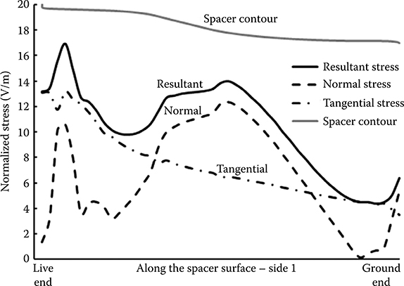
FIGURE 18.23
Electric field intensity along spacer surface on side 1 for resistive field.
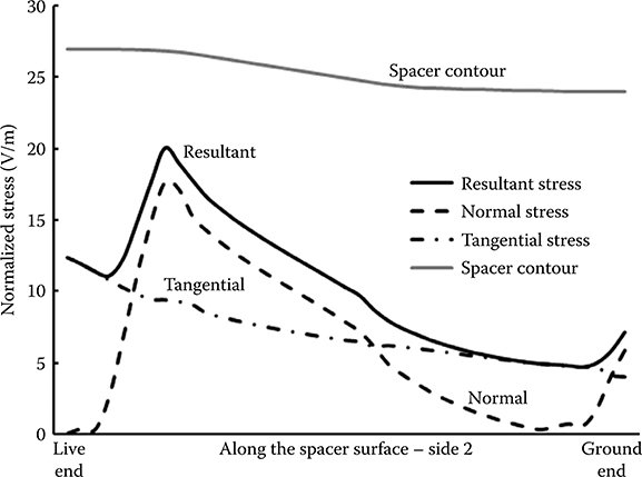
FIGURE 18.24
Electric field intensity along spacer surface on side 2 for resistive field.
Figure 18.24, on the other hand, shows that a resistive coating has favourable effect on field intensities on side 2 of the spacer as the maximum field stresses are reduced and the field stresses near the HV conductor are lower compared to the stresses in the mid-region of spacer surface on side 2.
Thus studies have also been carried out to determine the effects of resistive coating on any one side of the spacer. Figure 18.25 presents a comparison of resultant field intensity along the spacer surface on side 1 for three different cases: (1) uncoated spacer (capacitive field), (2) spacer coated on both sides by resistive layer of 107 Ω (resistive field) and (3) spacer coated on side 2 by resistive layer of 107 Ω. It may be seen from Figure 18.25 that coating only side 2 with a resistive layer increases the field intensity on side 1 compared to both capacitive and resistive fields. It should also be mentioned here that if only side 1 is coated with a resistive layer and side 2 is left uncoated, then the field intensities on side 1 of spacer surface are similar to the case when both sides are coated.
Comparison of resultant field intensity along the spacer surface on side 2 has been depicted in Figure 18.26 for three different cases: (1) uncoated spacer (capacitive field), (2) spacer coated on both sides by resistive layer of 107 Ω (resistive field) and (3) spacer coated on side 1 by resistive layer of 107 Ω. Figure 18.26 shows that field stresses for coating of side 1 only are almost the same as capacitive field. Hence, from Figures 18.25 and 18.26, it may be stated that if a resistive coating is to be used for field reduction, then both sides of the spacer should be coated with resistive layer.

FIGURE 18.25
Comparison of resultant field intensity along spacer surface on side 1.

FIGURE 18.26
Comparison of resultant field intensity along spacer surface on side 2.
In the case of high-voltage DC (HVDC) GIS, an additional problem arises in the form surface charging of spacer surface with time. The normal component of field intensity brings charges from gas insulation on to the spacer surface, which will get trapped on the surface if the surface resistivity is very high. Accumulation of surface charges reduces the normal component of field intensity, so that less and less charges are drawn to the surface. With passage of time, when the normal component of field intensity becomes nearly zero, then no more charges are drawn to the spacer surface and the surface may be stated to be fully charged in the absence of any surface resistivity [6]. Such accumulated surface charges change the field distribution around the spacer. In such cases, a resistive coating on the spacer surface is useful, as it helps in draining out the charges from the spacer surface [7,8].
Field computation for fully charged surface could be carried out with the boundary condition that Enor = 0 on the spacer surface [9], where Enor is the normal component of electric field intensity. Such field computation has been carried out for the spacer configuration under study. Figure 18.27 shows the comparison of resultant stresses on side 1 of spacer surface for three different cases: (1) capacitive field, (2) resistive field and (3) fully charged side-1 of surface. Figure 18.27 shows that the field distribution for fully charged surface is quite different from capacitive field, as the maximum field intensity is shifted close to the grounded enclosure. However, the maximum stress is not increased compared to capacitive field. The maximum stress is highest for resistive field, as shown in Figure 18.27.
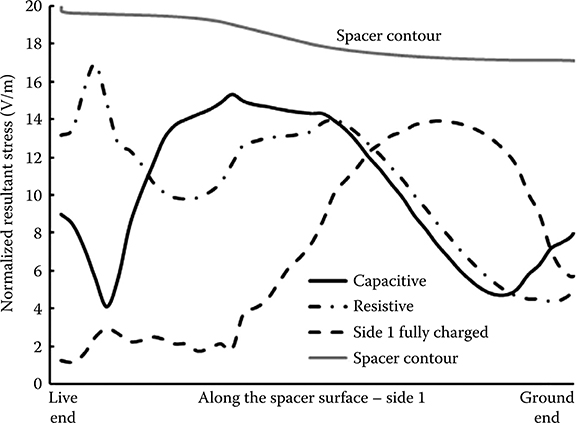
FIGURE 18.27
Comparison of resultant field intensity along spacer surface on side 1 for fully charged surface with capacitive and resistive fields.

FIGURE 18.28
Comparison of resultant field intensity along the spacer surface on side 2 for fully charged surface with capacitive and resistive fields.
Results of a similar study for side 2 of the spacer are shown in Figure 18.28. Figure 18.28 shows that full charging of side-2 of surface not only shifts the maximum stress near the HV conductor but also increases the value of the maximum stress significantly. The stresses for resistive field in the case of side 2 are comparatively lower for resistive field, as shown in Figure 18.28.
Objective Type Questions
1. Benchmark model commonly used for the validation of numerical codes for purely capacitive field analysis in two-dimensional system is
a. Cylinder in uniform field
b. Sphere in uniform field
c. Coated dielectric sphere in uniform field
d. Both (a) and (b)
2. Benchmark model commonly used for the validation of numerical codes for purely capacitive field analysis in axi-symmetric system is
a. Cylinder in uniform field
b. Sphere in uniform field
c. Coated dielectric sphere in uniform field
d. Both (b) and (c)
3. Benchmark model commonly used for the validation of numerical codes for capacitive-resistive field analysis in axi-symmetric system is
a. Cylinder in uniform field
b. Sphere in uniform field
c. Coated dielectric sphere in uniform field
d. Both (b) and (c)
4. A high-voltage cable termination typically provides
a. Adequate electric stress control
b. Comprehensive external leakage insulation
c. Proper sealing
d. All the above
5. Electric field distribution within a high-voltage cable termination is typically
a. Two-dimensional in nature
b. Three-dimensional in nature
c. Axi-symmetric in nature
d. None of the above
6. Commonly used method for stress control in a high-voltage cable termination is
a. Geometric stress control
b. Guard ring stress control
c. Capacitive stress control
d. Both (a) and (c)
7. Error in the numerical simulation of boundary occurs when a dielectric boundary meets a conductor boundary at
a. Very acute angle
b. An angle nearly equal to 90°
c. 90°
d. None of the above
8. For a numerical field computation, a post-type insulator is an example of
a. Two-dimensional case study
b. Three-dimensional case study
c. Axi-symmetric case study
d. None of the above
9. In the case of a post-type insulator, if the surface resistivity increases from a low value to a high value, then the power–frequency field distribution changes from
a. Resistive to capacitive–resistive to capacitive
b. Resistive to capacitive to capacitive–resistive
c. Capacitive to capacitive–resistive to resistive
d. Capacitive to resistive to capacitive–resistive
10. Free charges that are present around an insulator surface are drawn on the insulator surface by the
a. Resultant surface field intensity
b. Normal component of surface field intensity
c. Tangential component of surface field intensity
d. All the above
11. Movement of free charges on an insulator surface is caused by the
a. Resultant surface field intensity
b. Normal component of surface field intensity
c. Tangential component of surface field intensity
d. All the above
12. In the case of an outdoor porcelain insulator, which one of the following gives rise to highest field intensity on the outer surface?
a. No surface pollution
b. Uniform surface pollution
c. Partial surface pollution over a large area
d. Formation of dry band on the outer surface
13. The range of surface resistivity over the field distribution for an outdoor porcelain insulator changes from capacitive to resistive is lowest for
a. DC field
b. Power frequency field
c. Lightning impulse field
d. Switching impulse field
14. If a high-voltage conductor is to pass through an earthed barrier, then which one of the following is used?
a. Bushing
b. Pin-type insulator
c. Post-type insulator
d. Disc-type insulator
15. Accumulation of charges on the surface of an insulator
a. Increases normal component of surface field intensity
b. Decreases normal component of surface field intensity
c. Increases tangential component of surface field intensity
d. Decreases tangential component of surface field intensity
16. In the case of a high-voltage DC gas-insulated substation, if the surface of a spacer is fully charged, then which one of the following becomes zero?
a. Resultant component of surface field intensity
b. Normal component of surface field intensity
c. Tangential component of surface field intensity
d. All the above
Answers:
1) a;
2) b;
3) c;
4) d;
5) c;
6) d;
7) a;
8) c;
9) a;
10) b;
11) c;
12) d;
13) c;
14) a;
15) b;
16) b
Bibliography
1. A. Blaszczyk, ‘Computation of Quasi-static electric fields with region-oriented charge simulation’, IEEE Transactions on Magnetics, Vol. 32, No. 3, pp. 828–831, 1996.
2. S. Chakravorti and P.K. Mukherjee, ‘Power frequency and impulse field calculation around a HV insulator with uniform or non-uniform surface pollution’, IEEE Transactions on Electrical Insulation, Vol. 28, No. 1, pp. 43–53, 1993.
3. S. Chakravorti and H. Steinbigler, ‘Capacitive-resistive field calculation in and around HV bushings by boundary element method’, IEEE Transactions on Dielectrics & Electrical Insulation, Vol. 5, No. 2, pp. 237–244, 1998.
4. N.G. Trinh, F.A.M. Rizk and C. Vincent, ‘Electrostatic field optimization of the profile of epoxy spacers for compressed SF6 insulated cable’, IEEE Transactions on Power Apparatus and Systems, Vol. 99, pp. 2164–2174, 1980.
5. K. Itaka, T. Hara, T. Misaki and H. Tsuboi, ‘Improved structure avoiding local field intensification on spacers in SF6 gas’, IEEE Transactions on Power Apparatus and Systems, Vol. 102, pp. 250–255, 1983.
6. T. Nitta and K. Nakanishi, ‘Charge accumulation on insulating spacers for HVDC GIS’, IEEE Transactions on Electrical Insulation, Vol. 26, pp. 418–427, 1991.
7. F. Messerer, W. Boeck, H. Steinbigler and S. Chakravorti, Enhanced Field Calculation for HVDC GIS, Gaseous Dielectrics IX, Springer, New York/London, pp. 473–483, 2001.
8. F. Messerer and W. Boeck, ‘High resistance surface coating of solid insulating components for HDVC metal enclosed equipment’, Proceedings of the 11th ISH, London, Vol. 4, pp. 63–66, August 23–27, IEE (UK) Publication, 1999.
9. S. Chakravorti, ‘Modified E-field analysis around spacers in SF6 GIS under DC voltages’, Proceedings of the 11th ISH, London, Vol. 2, pp. 91–94, August 23–27, IEE (UK) Publication, 1999.